

Lab 4 - EE 421L
Lab Report - IV characteristics and layout of NMOS and PMOS devices in ON's C5 process
Lab description: Based on Tutorial 2, during this lab, we were to design schematics for a NMOS and PMOS, and simulate them to generate IV curves. Based on the MOSFETs, we then created layout connecting all terminals to probe pads. At then end, we LVS the layouts with their corresponding schematics.
1. Generating 4 schematics and simulations
As specified in the lab description, first a schematic for a NMOS device is generated with a 6u/600n width-to-length ratio. The cell was called 'NMOS_IV' Press 'i' to instantiate a nmos4 from NCSU_Analog_Parts library (do not choose nmos due to it can cause LVS problems). Then, dimensions are specified: width=6um and length=600nm. (see below, left)
Note that 3 pins are connected to gate, drain, and source, and the body is grounded. From this, a symbol of the schematic is created (Create ->Cellview->From Cell view -> OK) see above, right.
Now, let's create a schematic to simulate ID vs VDS (cell sim_NMOS_IV)

Hit 'Check and Save' to show that there is no errors in the schem.

First, I simulated for VGS varying from 0 to 5v in 1v steps and VDS from 0 to 5v in 1mV steps. Select current at node D as output (ID). In the choosing anaylis window, DC simulation is set for sweep range VDS from 0 to 5, step size 1m. Go Tools-> Parametric analysis and set VGS from 0 to 5 in 1 step, and then press Run. The following 6 plots appears for the 6 different values set for VGS:

Next, I simulated ID vs VGS for VDS=100mV and VGS from 0 to 2v in 1mV steps. (see below)
 Lab4_pictures/PMOS_LVS2.JPG
Again, same output as before is choosen, and DC simulation is set for VGS from 0 to 2 in 1m step. Then, run it.

The second part of the lab was creating a schematic now for a PMOS device (cell PMOS_IV). Again, pmos4 is used, not pmos. (see below, left) Width=12um and Length=600nm are set.


All pins are connected to its corresponding terminal (G:gate, S:source, D:drain, and B:body). A symbol is created for this PMOS (see above, right).
The schematic for simulation is design as seen below (cell sim_PMOS_IV)

Following the same procedure as NMOS, I first simulate ID vs VSD for VSG from 0 to 5v in 1V step and VSD from 0 to 5v in 1mV step.

Then, the schematic is modified and set VSD=100mV and VSG from 0 to 2V in 1mV steps.

This schematic was used to plot ID vs VSG. Following the same procedure as before, I obtained:

2. Layout and LVS 6u/0.6 NMOS and 12u/0.6u PMOS using probe pads
Now, it is time to layout both the NMOS and PMOS, but, as specified in the lab, all 4 terminals are connected to probe pads. So, to begin with a layout a probe pad (cell probe_pad)
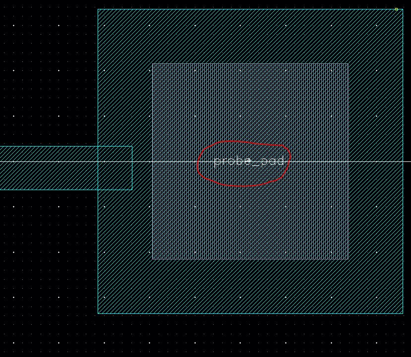
This probe pad (see above), according to the rules, is built in metal3 layer and is 33.6umx33.6um. The glass layer is 21.6umx21.6um.
A schematic and symbol of the probe pad is then created.


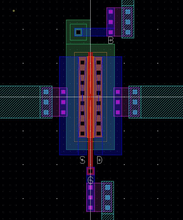
Next, in NMOS_IV cell, to layout a NMOS, press 'i', in the NCSU_TechLib_ami06 library, select nmos, and specify width=6um and length=0.6um. After the NMOS is place, 4 prode pas are connected to its 4 terminals via connections from metal1 to metal2, and from metal 2 to metal 3.

Zooming in to appreaciate the NMOS,

To do LVS, layout extraction is needed. Go Verify-> Extract->OK (Don't forget doing DRC first). Zoomed view shown below on the right to show NMOs parasitics.


The previous NMOS schematic is modified by addin the 4 probe pad symbols to each of the 4 terminals.

DRC to show no errors. On the layout, go Veriry-> LVS. Add the schematic and extracted view, and hit Run (see below, left).


It is seen that both netlist match. To make sure, the output window is shonw above on the right.
Then, I did the same for the PMOS device. In the layout, in the NCSU_TechLib_ami06 library, I picked 'pmos'. Width=12um and Length=600n. The layout is shown below with the 4 probe pads connected throuhg metal1, metal2, and metal3

Zooming in for a better looking of the PMOS,
The extracted view is obtained (below, left). It was zoomed in to show parasitics (below, right)


The corresponding schematice for this PMOS was also modified by addin 4 probe pads to each terminal.

DRCing and going back to the layout, LVS is performed (Verify -> LVS).

It is shown above that the netlists match for both the schematic and extracted view.
All the cells mentioned on report are found here.
--------------------------------------------------------------------
As always, I back up all my work to my flashdrive and Google drive account.

Return to EE421L - Student Lab Reports