Lab 3 - ECE 421L 

Authored by Stephanie Silic,

silics@unlv.nevada.edu

September 21st, 2015 


Description of lab:


For this lab, we are creating a layout of the 10-bit Digital-to-Analog Converter (DAC) designed in lab 2, using 10k resistors.


Prelab:


  1. Back up all work
All work backed up in Google Drive: 
 http://cmosedu.com/jbaker/courses/ee421L/f15/students/silics/Lab3/prelab_backup_snip.JPG
 
  1. Finish Tutorial #1
  We left of  the tutorial after creating the voltage divider below:
 
 http://cmosedu.com/jbaker/courses/ee421L/f15/students/silics/Lab3/10k-divider_sch.JPG
 
 Now, our task is to use the n-well layer to lay out n-well resistors to implement the divider.
The 10k resistor is shown below (details on its construction in the lab report):
   
http://cmosedu.com/jbaker/courses/ee421L/f15/students/silics/Lab3/layout_10k_res.JPG
 
 
After creating a new layout cell view, and instantiating two 10k resistors and connecting the pins with Metal 1, we have the voltage divider as follows:
 
http://cmosedu.com/jbaker/courses/ee421L/f15/students/silics/Lab3/10k_divider_layout.JPG
   
Finally, we DRC the layout, extract it, perform LVS, and simulate the extraced view:
 
http://cmosedu.com/jbaker/courses/ee421L/f15/students/silics/Lab3/10k-divider_sim.JPG
 
 The output is what we expect from the voltage divider with an input of 1V.
This completes Tutorial 1.

 
 Lab Report: 
 
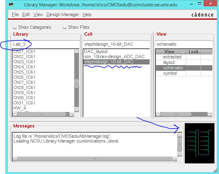
For Lab 3, we have to construct the layout of the DAC designed Lab 2 (my lab 2 report here).To begin the layout, a new library must be created, then the DAC schematic created in Lab 2 copied into it. Once that is complete, we can create a new layout cell view and begin the layout of the DAC using a resistor ladder network. The full library for lab 3 is shown below:
 
http://cmosedu.com/jbaker/courses/ee421L/f15/students/silics/Lab3/snip1_Lab3_library.JPG
 
Layout of a 10k resistor:
 
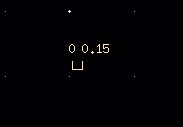
To create a resistor of a certain value using the n-well, we must set the length and width of the n-well according to the process information from MOSIS. The sheet resistance of the n-well is 800 ohms per square. Thus, the total resistance of our n-well resistor will be 800 (L/W). But the minimum width according to MOSIS C5 process is 3.6um. However, we also need to keep in mind the grid is .15 um:
 
 http://cmosedu.com/jbaker/courses/ee421L/f15/students/silics/Lab3/snap_grid_size.JPG
 
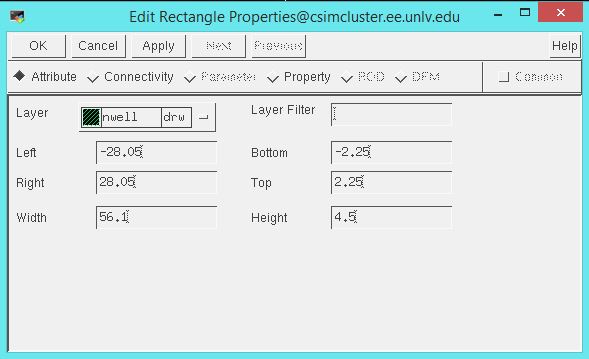
We must have the n-well line up on the .15um grid. So as in Tutorial 1, we can set the width to 4.5 um (divisible by .15), and adjust the length to be 56.1 (adjusted from 56 so it's divisible by .15).
  
http://cmosedu.com/jbaker/courses/ee421L/f15/students/silics/Lab3/L-and-W-of-10k.JPG
 
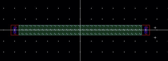
After extracting the n-well resistor, we can check its value by zooming in on the left side of the extracted view:
 
http://cmosedu.com/jbaker/courses/ee421L/f15/students/silics/Lab3/Tutorial1_10k_extracted.JPG
   
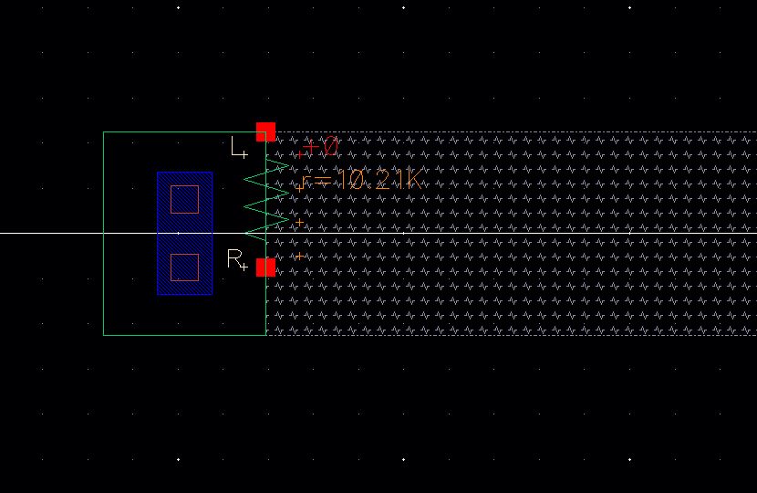
The value is 10.21k, which is close enough to 10k for us.
 
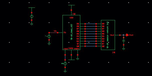
Using this n-well resistor in the layout of the DAC:
 
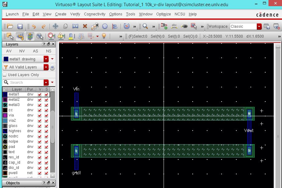
To begin with, three resistors are instantiated to create the basic R-2R cell, which we can copy in an array of 9. Each resistor in the DAC is laid out in parallel having the same x-position but varying y-positions. The bottom cell must be connected to the bottom resistor, then to ground. All input and output pins are on metal 1 (seen here for B0 and gnd!):
 
http://cmosedu.com/jbaker/courses/ee421L/f15/students/silics/Lab3/snip3_layout_bottom-cell.JPG
 
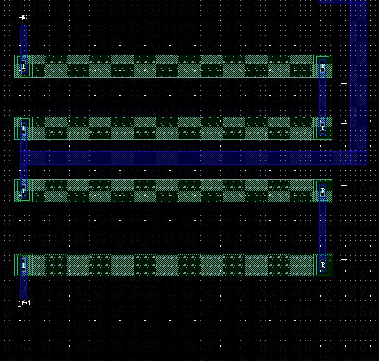
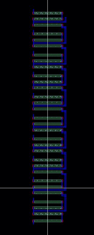
 The entire DAC looks like this:
 
 http://cmosedu.com/jbaker/courses/ee421L/f15/students/silics/Lab3/snip2_entire_layout.JPG
 
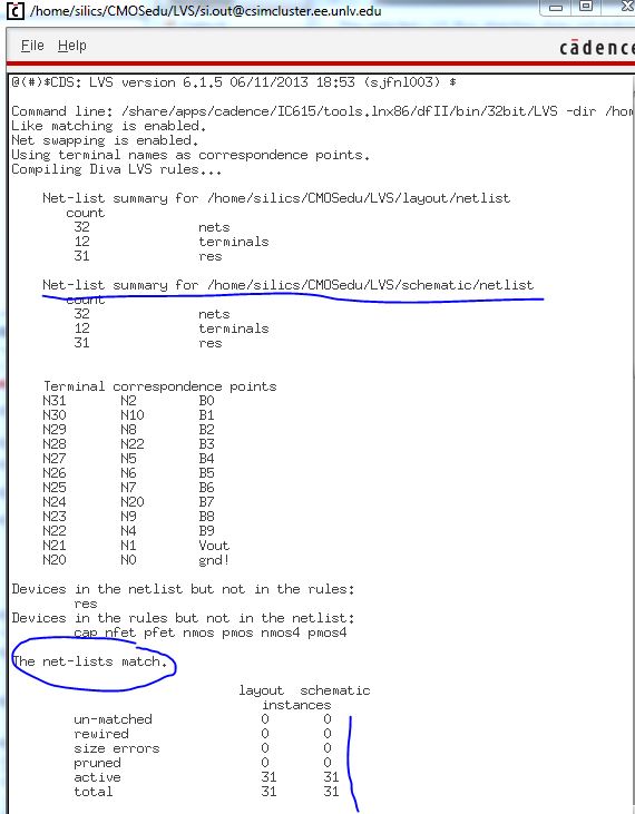
Now, we have to DRC, extract the layout, and perform the LVS.
 
The LVS was successful:
 
http://cmosedu.com/jbaker/courses/ee421L/f15/students/silics/Lab3/snip5_LVS_net-lists-match.JPG
 
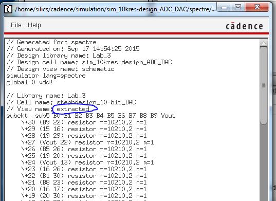
Finally, we can simulate the extracted view of the layout by going to our sim_10-bit DAC cell and selecting Setup -> Environment and adding the word "extracted" before "schematic in the window:
 
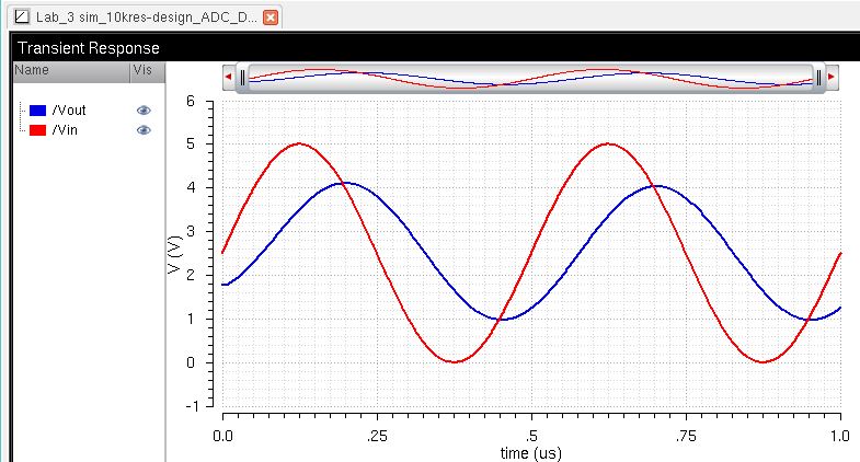
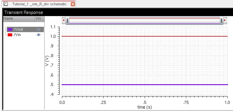
The simulation is as follows:
 
http://cmosedu.com/jbaker/courses/ee421L/f15/students/silics/Lab3/snip4_first-sim.JPG
 
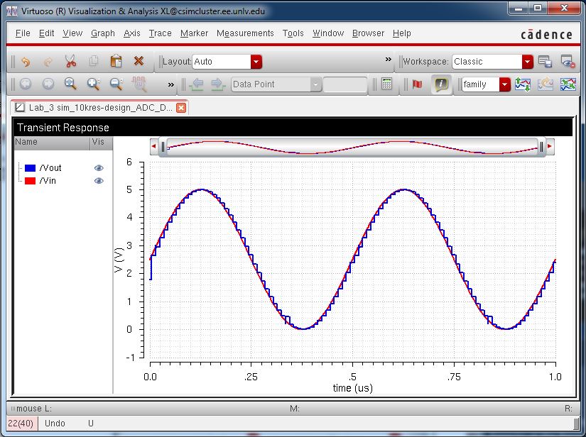
This simulation looks like it was successful, since it matches what was simulated with the schematic in Lab 2.
 
But just to be sure we are simulating the extracted view, we check by selecting Simulation -> Netlist -> Display and checking to see that it shows the simulation is really from the extracted view:
 
http://cmosedu.com/jbaker/courses/ee421L/f15/students/silics/Lab3/snip6_sim-of-extracted-for-sure.JPG
 
As we can see, the simulation was indeed from the extracted layout, and thus our layout of the DAC is operating as it should.
 
To smooth out the output of the DAC, we add a 10pf capacitor to the output, as seen below:
 
 http://cmosedu.com/jbaker/courses/ee421L/f15/students/silics/Lab3/snip7_schematic.JPG
 
The simulation, again from the extraced view, is as follows:
 
 http://cmosedu.com/jbaker/courses/ee421L/f15/students/silics/Lab3/snip8_second-sim.JPG
 
Once again, the simulation with our extraced layout agrees with the original simulations performed in lab 2. 
 
Final design directory zipped here.


return to my labs

return to EE 421L page