Lab 2 - ECE 421L
Authored
by Stephanie Silic
silics@unlv.nevada.edu
August 29th, 2015
Pre-Lab
1) Narrative of pre-lab steps:
To
begin, I read through this entire lab write-up, then downloaded the
lab2.zip file and unzipped it in the CMOSedu directory using MobaXterm.
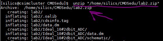
This
archive contains a simulation example using an ideal 10-bit
Analog-to-Digital Converter (ADC) and Digital-to-Analog Converter
(DAC).
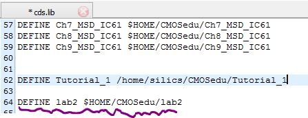
Next, we add the statement DEFINE lab2 $HOME/CMOSedu/lab2 into the cds.lib in the CMOSedu directory:
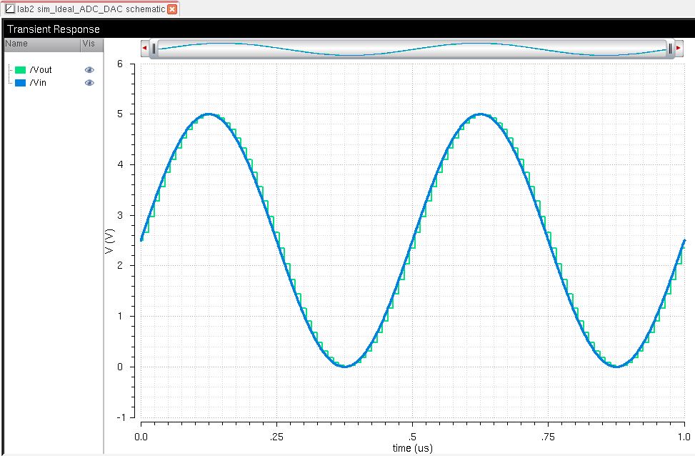
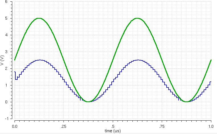
Now we can start Cadence and simulate the example and analyze the operation of the schematic (shown below).
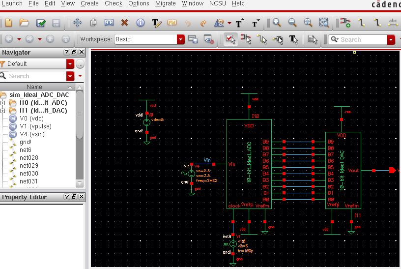
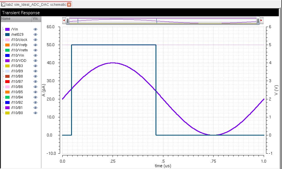
First off, the simulation without any changes is shown with the color and size of the traces changed for clarity:
2) discussing simulation results different from the above to illustrate understanding of the ADC and DAC
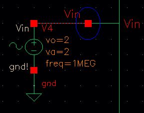
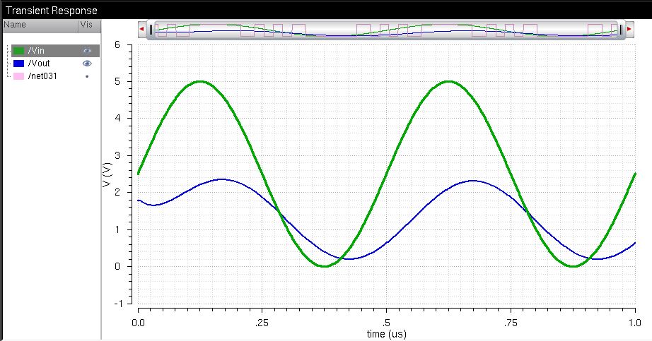
To get different simulation results, we can change the
values of the input sine wave. Instead of an offset and amplitude of
2.5V, I changed the offset and amplitude to 2.0V, and the frequency
from 2 mHz to 1 mHz.
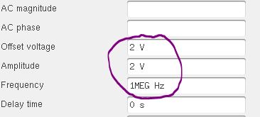
The result looks like this:
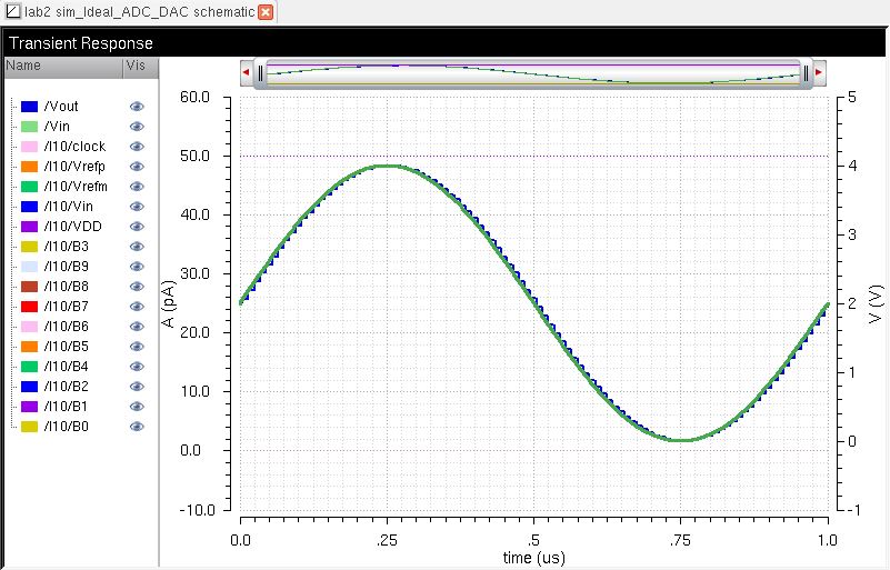
The
Analog-to-Digital Converter (ADC) takes the analog signal (sinusoid)
and 'translates' it into a series of digital code. These 10 bits
can be seen listed on the left of the above image, with B0 being on the
bottom of the list, with a yellow trace color.
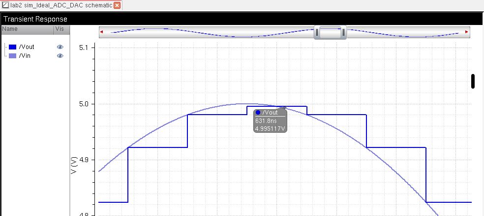
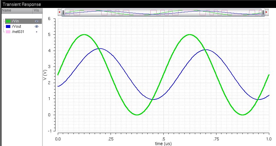
Below is
the most significant bit (MSB), which is B9, shown with the input
analog signal. It is easiest to see how the MSB can be a part of a
digital representation of a sinusoid:
3)
Explaining how to determine the least significant bit (LSB, the minimum
voltage change on the ADC's input to see a change in the digital code
B[9:0]
The least significant bit (LSB) is defined as the smallest possible change in the analog output voltage, or mathematically:
1 LSB=Vref/2^n
In this case used in the first example, the LSB = 2.5V/1024 bits = 2.44mV/bit
All work backed up in Google Drive:
Lab Procedure:
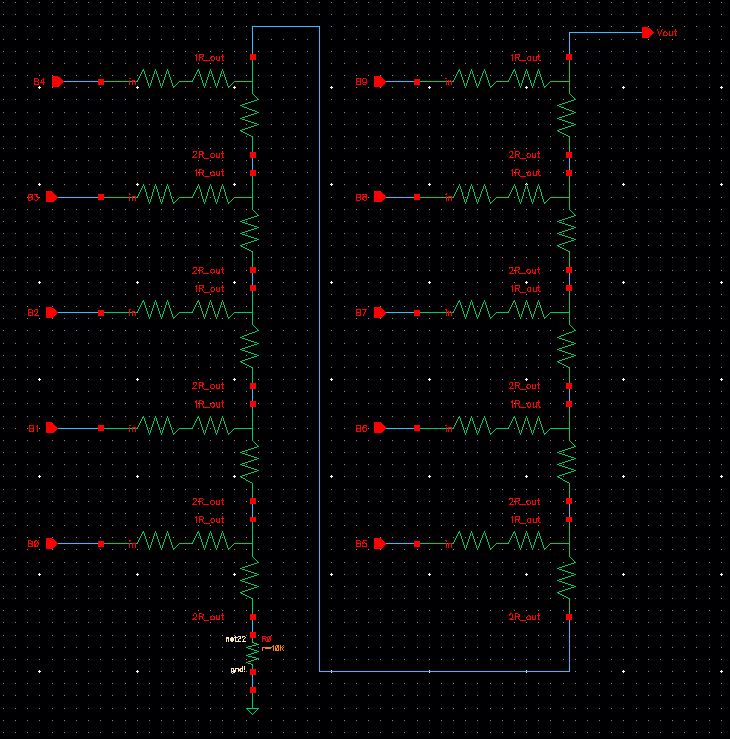
- Design of a 10-bit DAC using n-well resistors of value 10k
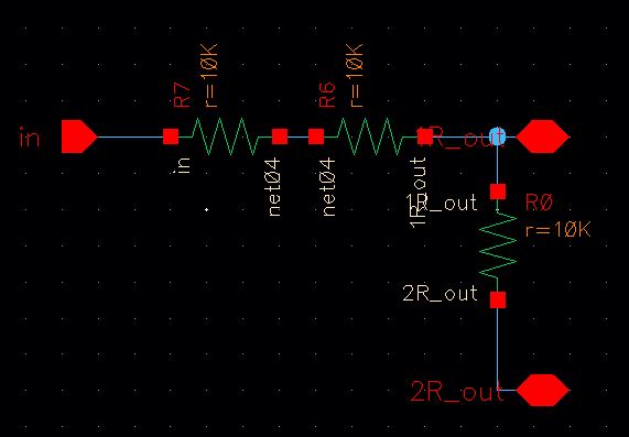
For the lab procedure, the first step was to draft a design for a
Digital to Analog Converter implemented with n-well resistors and
following the template given. The design is a simple R-2R network, made
up of cells comprised of three 10k resistors in series, shown
below:
From this schematic, a symbol is made and the larger circuit is constructed as follows:
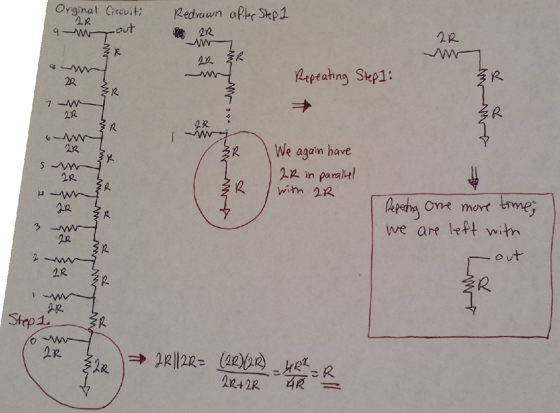
- How to determine the output resistance of the DAC:
The
2R resistors at the bottom of the resistor ladder are in parallel;
2R||2R = R, and that R adds with the R above to become 2R.
This 2R
is again in parallel with the next 2R branch up the ladder, and can be
once more simplified to R. This process repeats until
we are only left with R:
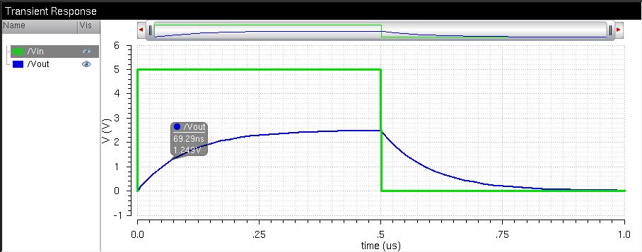
The
delay when the DAC has only one step input on B9, with B0-B8 grounded
and a load of 10pF should be 0.7(RC)=0.7(10k)(10p)=70ns.
To verify this delay time, I set up the following circuit using the newly designed DAC:
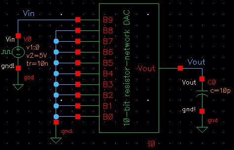
The simulation is as follows:
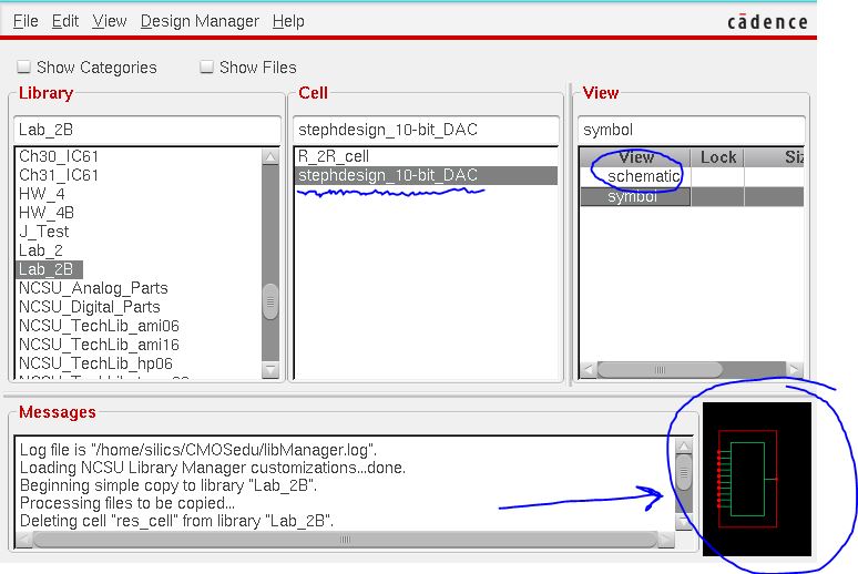
- How to create a symbol view for the DAC design with the same footprint as the Ideal DAC
To make it easy to create a symol view that has the exact same
footprint as the Ideal 10-bit DAC given in the prelab, the Ideal DAC
was copied over to my own Library created for Lab 2, and the entire
schematic shown above was created inside that cell. An image from this
process is shown below:
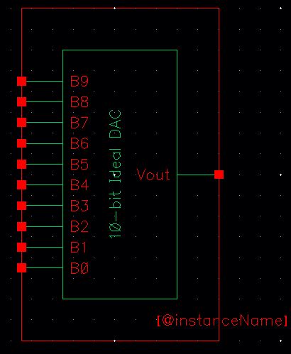
Now,
for this design, the VDD, Vrefp, and Vrefm were not needed for the DAC,
so those inputs were deleted. Thus, we are left with input pins 0
through 9 and one output pin:
- Simulations to verify the design functions correctly
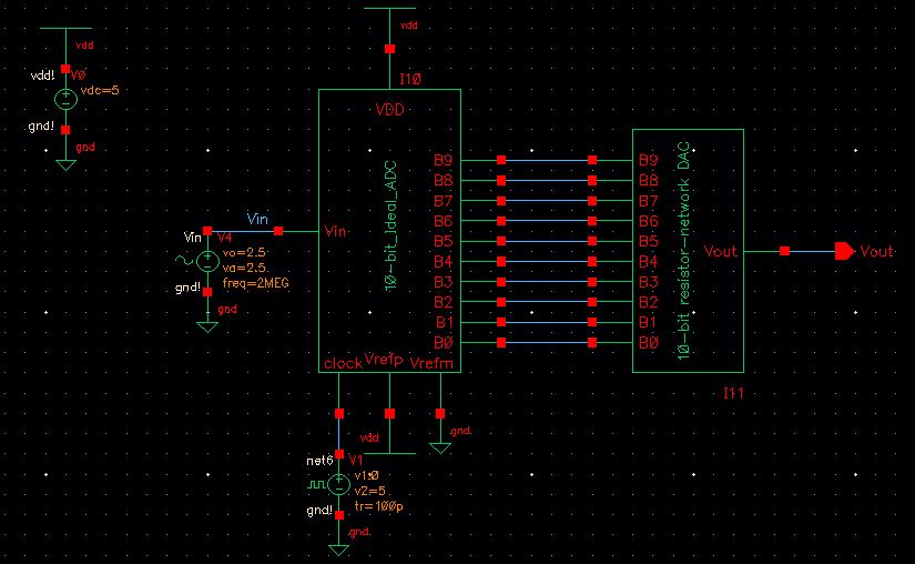
To
simulate this design in the ADC-DAC schematic, I first copied the
sim_Ideal_ADC_DAC to another cell in my Lab 2 Library, and then deleted
the Ideal DAC from that schematic, replacing it with my resistor-based
DAC. Thus, we have the following schematic:
To ensure my DAC works, the simulation is run:
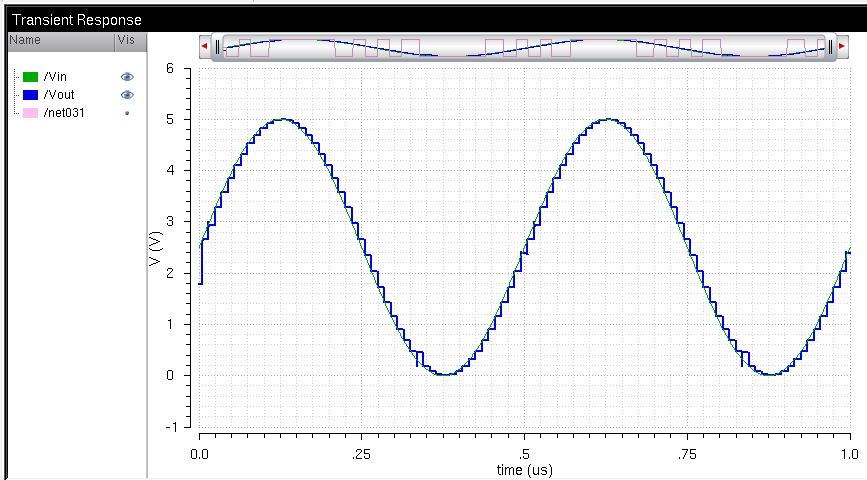
Yes!
The results show that the DAC works as expected; this simulation looks
like the one simulated in the prelab with the Ideal DAC. Since my
simulation was having convergence issues, I had to force convergence by
setting the parameters in Simulation -> Options -> Analog. Thus,
the simulation will not be as accurate as it could be.
When the DAC drives a 10K load, we get the following simulation:
With a 10k load, the output is exactly 1/2 of the input, since the
output resistance of the ladder (calculated previously) is R, which in
our design is 10k, and we are left with a voltage divider with equal
resistor values. So vout= vin times 10k/(10k+10k)=1/2vin. The
simulation above confirms this, since the peak output is about 2.5V.
Adding a 10pF capacitor results in the following plot:
The output looks much neater and sinusoidal than before, with just a resistive load.
Finally, what happens if the DAC drives a load of just a 10pF capacitor? The following simulations shows us:
This result appears very like the output of an RC circuit.
- Discussion of what happens if the resistance of the switches in a real circuit aren't small compared to R
If
the switches in a real circuit have a large resistance compared to R,
then the 2R portion of the ladder will have a large resistance in
series with it. When we calculate the equivalent resistance of this big
resistance in parallel with 2R, we have (2R)(2R)/(large R+2R).
The equivalent resistance will be less than R, which will decrease the output.
Once again, all my work is backed up in Drive:

Return to EE421L Fall 2015 page
Return to my labs