Project - ECE 421L
Authored
by Jared Hayes
hayesj18@unlv.nevada.edu
November 23, 2015
Description:
Design schematics, symbols, and simulations of the following in preparation for implementation on a chip:
1) a 25k resistor using the n-well (connect between 2 pads but we also need a common gnd pad)
2) a voltage divider between a 25k resistor and a 10k resistor
3) An inverter made with a 6/0.6 NMOS and a 12/0.6 PMOS
4) a PMOS transistor measuring 6u/0.6u where all 4 terminals of each
device are connected to bond pads (7 pads + common gnd pad)
5) an NMOS transistor measuring 6u/0.6u where all 4 terminals of each
device are connected to bond pads (7 pads + common gnd pad)
6) a NAND gate using 6/0.6 NMOSs and PMOSs
7) a NOR gate using 6/0.6 NMOSs and PMOSs
8) 31 stage ring oscillator with a buffer for driving a 20pF off-chip load
9) 8-bit resettable (with clear) up/down counter (with buffered outputs)
Pre-lab
Make sure you understand all of the Cadence tutorials on CMOSedu here.
Lab Report:
25 K Resistor
Create
a 25k n-well resistor. This is the same resistor created in
tutorial 1. Run a DC sweep and plot the IV curve. The
simulation shows 200uA flowing through the resistor at 5V.

Simulation Circuit | 
Simulation Results |

 25k N-Well Resistor Layout 25k N-Well Resistor Layout |
In
a later lab, all of the components will need to be connected to pads,
being sure to use an appropriate amount of vias. The 25k resistor
is shown connected to two pads below as an example.

Voltage divider
The voltage divider that was created and used in lab 2 and tutorial 1 includes a 25k followed by a 10k resistor. Below is the schematic and simulation results for the 25k,
10k voltage divider. With an input of 5V, the expected output is
5*(25K)/(10K+25K) = 3.75V.

Voltage divider schematic
|

Simulation results | |

 Voltage Divider Layout Voltage Divider Layout | |
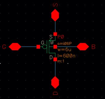
NMOS Transistor
Below is the schematic, symbol and the IV characteristic curves for a 6u/.6u NMOS transistor. The four terminals will be connected to four pads, one being the common ground pad.
PMOS Transistor
Below
is the schematic, symbol and the IV characteristic curves for a 6u/.6u
PMOS transistor. The four terminals will be connected to four
pads in the final chip layout.
Schematic for PMOS Device | 
Simulation Circuit for PMOS Device |

ID Versus VSD (Stepping VSG) | 
ID Versus VSG |

PMOS Layout
|
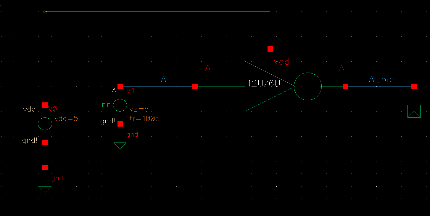
Inverter 12u/6u
Below
is the schematic and simulation of a 12u/6u (12um W PMOS, 6u W NMOS,
600n L) inverter. Note that there is a vdd pin instead of a
global vdd like in the earlier labs/tutorials.

Inverter Schematic | 
Inverter Symbol/Simulation Schematic
Inverter Layout


|

Simulation Results |
| |
NAND/NOR Gates - 6u/.6u MOSFETS
Below
is the schematics and simulations for both the NAND and NOR gates.
These were also already created from previous labs, but with VDD
pins instead of a global VDD. This is to ensure that each
circuit
has
a dedicated vdd pad. The NAND gates output goes low when both
inputs are high and the NOR gates' output goes high when both inputs
are low.
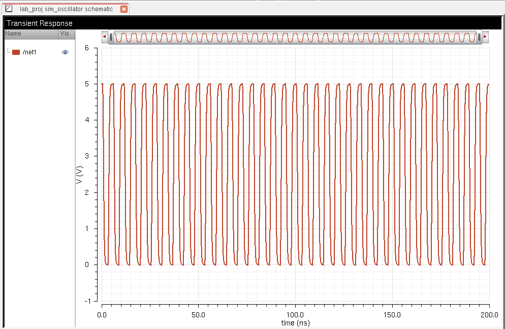
31 Stage Ring Oscillator
Below
is the schematic and simulation of a 31 stage ring oscillator with an
output buffer driving a 20pF load. There are two large inverters
following the buffer so that it can drive a
20pF load. The period is about 5ns, which translates to a frequency of
200Mhz. This was created from the ring oscillator in tutorial 5.
| Schematic | 
Simulation of Ring Oscillator |

Simulation Results |  |

8-Bit Resettable Up/Down Counter
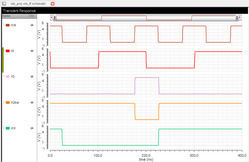
D-Flip-Flop
Below is a CMOS D flip flop
with a clear. The asynchronous clear is implemented using NAND gates.

Schematic of resettable DFF | 
Simulation Circuit for DFF |

Simulation |  |

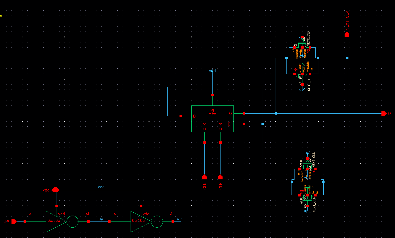
Up-Down Counter

Single Bit of Up/Down Counter

| 
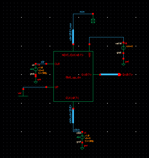
Schematic/Simulation of 8 Bit Up/Down Counter

|

8-Bit Up_Down Counter Layout |
Use
the knowledge gained in tutorial 5 to instantiate the single bit
counter 8 times. The output Q or Q' will be fed into the clock of
the next flip flop.
When
the Up_Dn input is at VDD the counter will count up and when it is at
ground it will count down. Also when CLR is high, the counter
will reset all of the flip flops to
0 and start up or down counting from 0 once the CLR signal goes low.
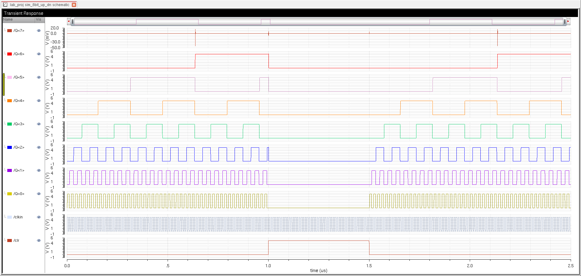
Below
is the simulation showing the counter counting down, up, and clearing in that order.
It's best to use Ultrasim for this, unless you want to wait for a
long time.
Counter Full Operation |
 |
The
outputs of the counter need to be buffered before connecting to a pad.
I use 12u/6u width inverters with multipliers of 8 and 64 to
create a buffer consisting of a 96u/48u inverter and a 768u/384u inverter.


Backup:
Cadence files and lab report are automatically backed up in my Dropbox folder.


The cadence files can be found here: projJH_f15.zip
Return
to the directory listing of students in EE 421L, Fall 2015
Return to the EE421L
Fall 2015 webpage
return


