Lab 3 - ECE 421L
Degracia, Manuel C.
degracia@unlv.nevada.edu
14/21 September 2015
Pre-Lab
Overview
Pre-lab consists of finishing Tutorial #1 from where we left off in Lab #1 (25th image of tutorial).
Continued Process
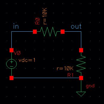
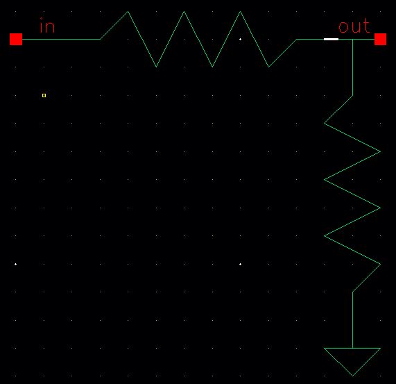
*Schematic of where we last left off in the tutorial.
7.
From the given schematic shown above, we want to create a general
purpose schematic which will make it more useful as a cell in an
integrated circuit. To do so, delete Vdc and the two wires connected to
it and create two pins called in and out. Within the parameters of each pin, make sure each one has the appropriate direction (in = input, out = output).
Check and Save to verify the schematic has no errors.
8.
Create a symbol for this schematic so it can be used in later designs.
(Create > Cellview > From Cellview). Follow through with the
symbol generation window making sure the pin specifications are
correct. Once done, the following generic symbol will be displayed.
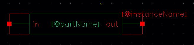
9. Delete everything in the symbol except for the in and out pins and wires.
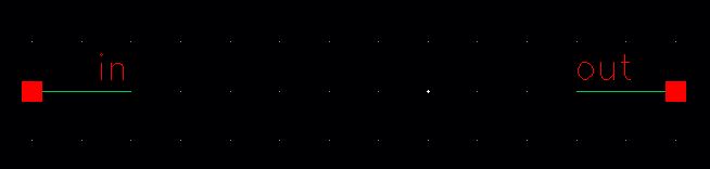
10.
Move the pins and lines further apart. Using the draw line command
(Create > Shape > Line), draw a generic form of a resistor and
ground.
Check and Save the symbol to verify if there are any errors.
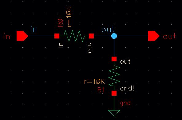
11. Simulate the cell's operation to verify it runs properly. Afterwards, create a copy of R_div into another cell called, sim_R_div. Within the sim_R_div cellview, delete spectre_state1 because it is not needed.
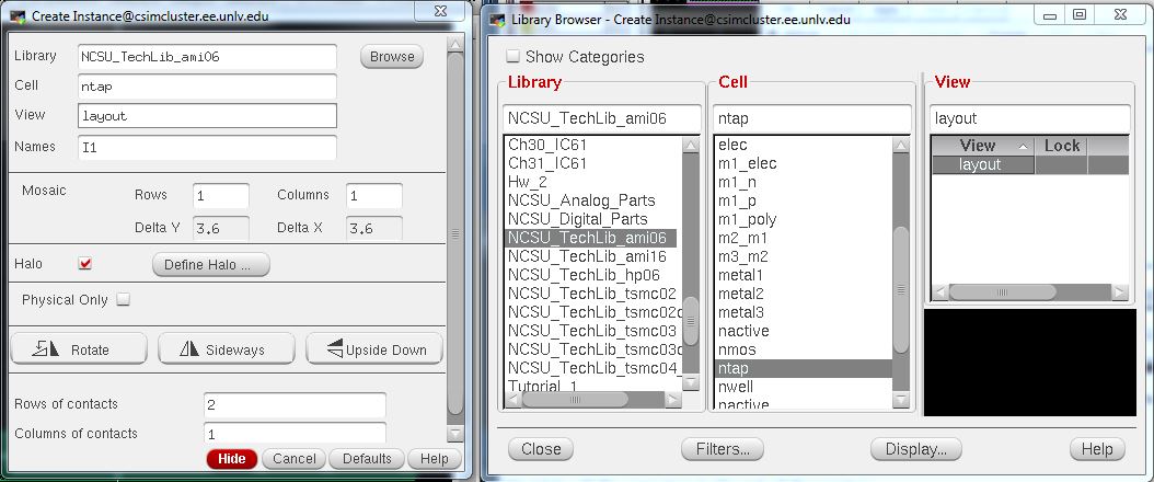
12. Open the schematic view of sim_R_div and delete everything in the cell. Next add the R_div symbol using instance (i) and locating the symbol in the Tutorial_1 library found in the component browser. Create the schematic seen below.
Check and Save to verify there are no errors.
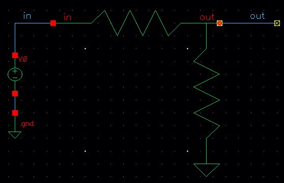
13. In this case, 2 errors will be found.

14. Use the following to determine where the issues are located and details about the warnings. (Check > Find Marker)
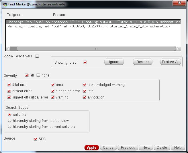
The floating wires are intentional, thus click Ignore twice and Check and Save again. You'll find that there are no errors or warnings.
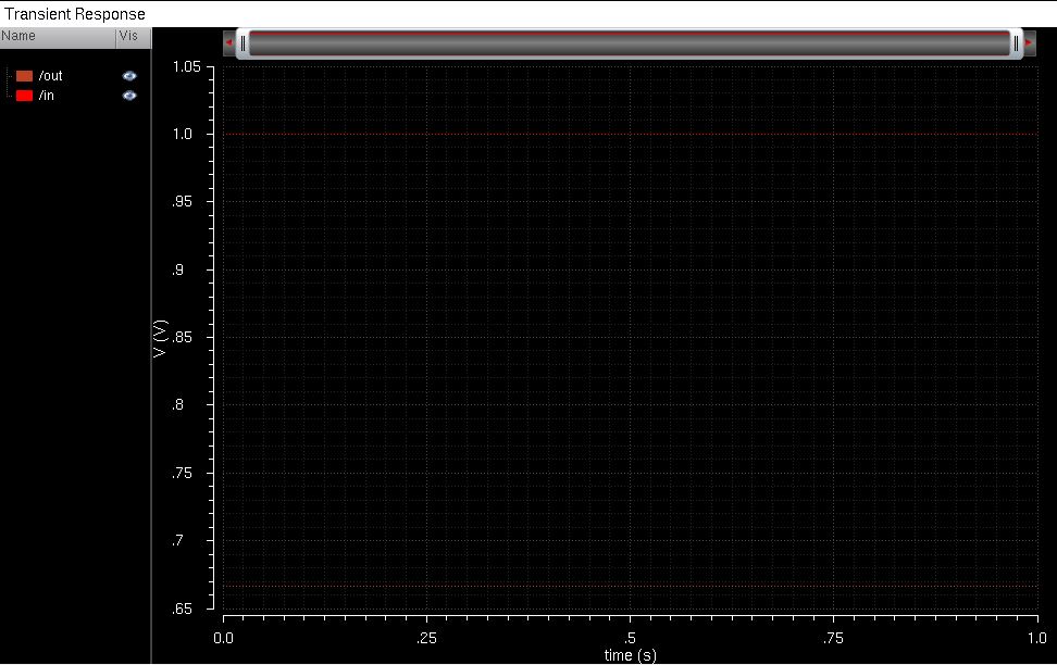
15. Simulate the circuit by launching ADE and then load the state. The following transient response should be shown.
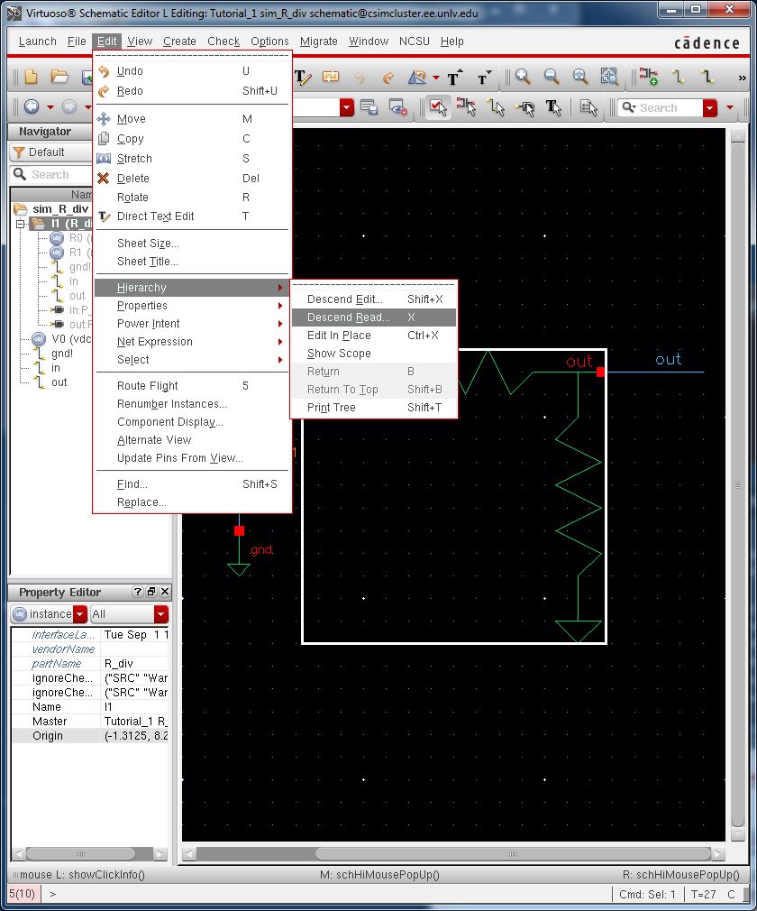
16. As a quick side tutorial on hiearchy, by clicking the R_div symbol and pressing X, one can descend into the hiearchy. In addition, pressing b
will bring you back up into the hiearchy. If hotkeys are not favorable,
one can still follow through the menu options. (Edit > Hierarchy
> ...)
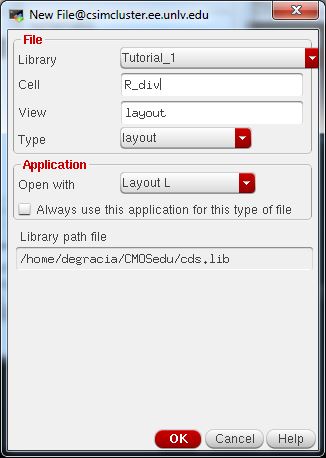
Create the layout of the resistive divider
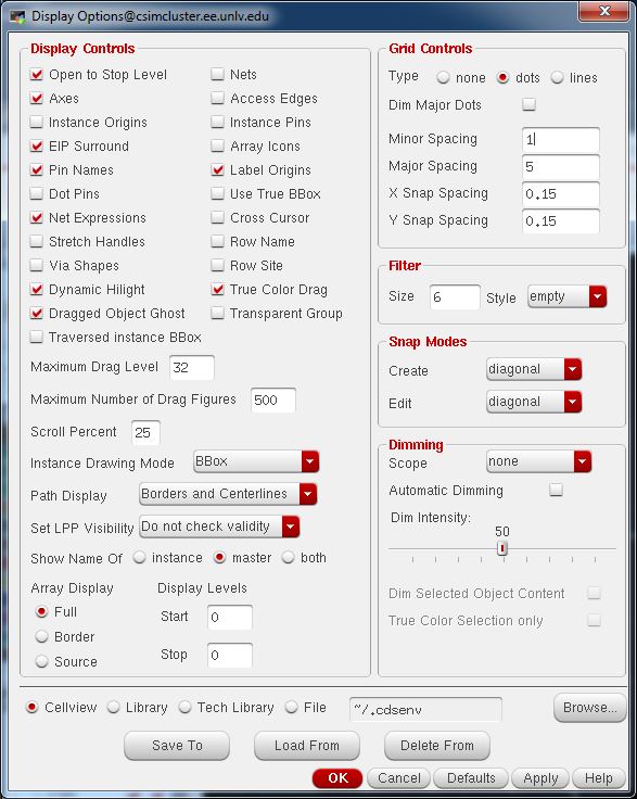
17. Make a new cellview for the layout of R_div.
18. Setup the following items within the Display Properties (e):
- Set the display so that Pin Names are shown.
- Change the Snap Modes to Diagonal.
- Side note: Know how and when to change the Stop Level to see more details in different levels.
Creating the layout for the 10k Resistor
- We will use the n-well layer for the 10k resistor.
- The sheet resistance of n-well in the C5 process is roughly 800 ohms.
- The
minimum width of the n-well is 12 lambda (3.6 microns since lambda here
is 300nm) so lets make a 10k resistor using a width = 4.5um and length
= 56um.
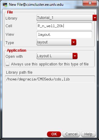
19. Create a new cellview called R_n_well_10k.
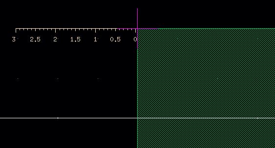
20. In the n-well layer, draw a generic rectangle (Create > Shape > Rectangle).
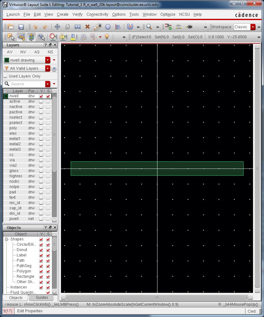
21. Click on the rectangle and press q
to edit the parameters (Edit > Basic > Properties). As calculated
above, we want a resistor that is 56um long and 4.5um wide.
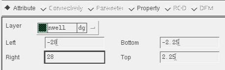
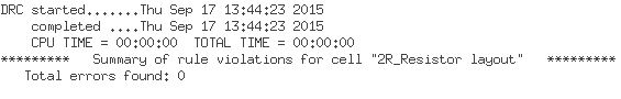
22. Design Rule Check the layout (Verify > DRC).
After running DRC, 4 errors will be found.
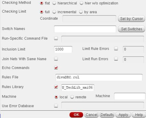
23. Use Find Marker again to pinpoint the errors and details regarding them.
24. The issues revolve around the rectangle not being snapped to the y-axis grid. To resolve this issue, we can use a ruler (k) to determine the proper X & Y Snapping measurements and change the values in the Display Parameters (e).
25. Add connections to the ends of the resistors and add pins to each side in the metal1 layer (Left side = L, Right side = R). To do so, follow the steps shown:
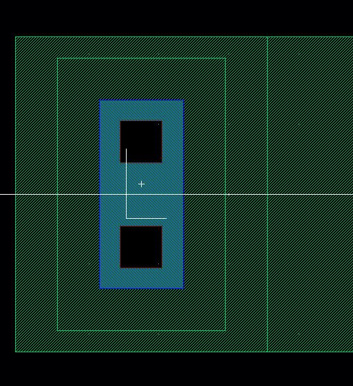
Each corner should be similar to the left ntap displayed.
26. Turn the Gravity On control off for easier moving of parts (E) and change the Stop Time to 10 (e) so more layers can be seen.
27. Move onto the res_id layer and draw a rectangle in between the two ntaps.
28. Extract the layout to determine the resistance value (Verify > Extract).
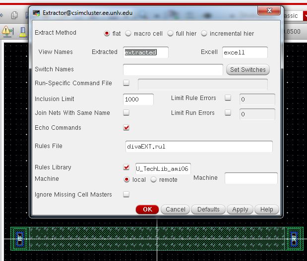
29. Once extracted, open up the extracted view found in the Library Manager and zoom in to see the resistor value.
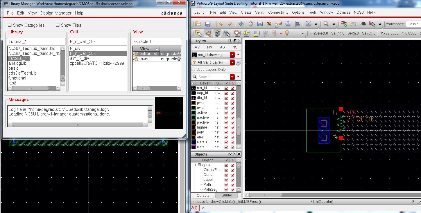
Save and Close the layout view of the resistor.
Drawing the layout of the R_div cell
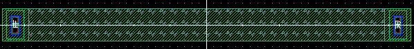
30. Open the layout view of the R_div cell and instantiate two 10k n-well resistors. Then, DRC to make sure that they are far enough apart.
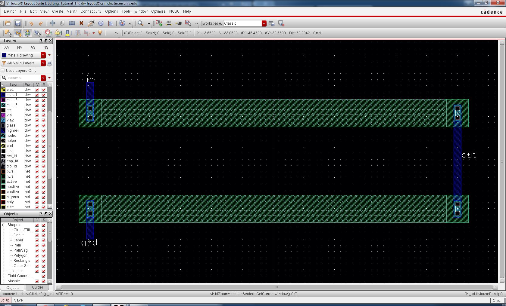
In the metal1
layer, add rectangles to connect the resistors together and to connect
to the Pins of the resistors. In addition, add Pins to each
corresponding rectangle as displayed above.
31. Do the following:
- DRC layout to verify there are no errors or warnings.
- Extract layout
- LVS
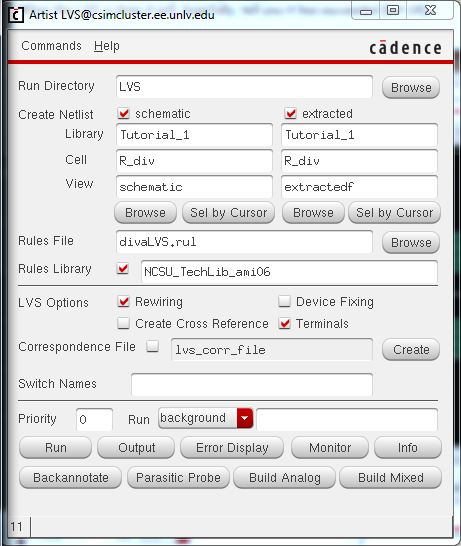
32. Once LVS is completed, click Output to see if any problems or errors have occurred. In this case we have three issues.
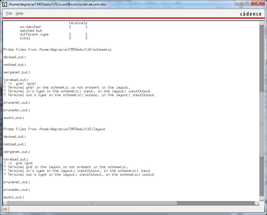
As displayed, there are issues with Pin Names and Pin directions (gnd = gnd!, in = input, out = output).
33. Once fixed, repeat steps #31-32.
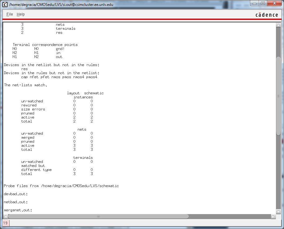
From this, we can finally see that there are no errors or problems and the netlists MATCH! This concludes Tutorial #1.
Back-Up Files
As always, it is always important to backup files by either creating a
folder on your personal computer, emailing the files to yourself and/or
backing it up on a cloud (dropbox, icloud, google drive).
Post-Lab
Overview:
- Use the n-well to layout a 10k resistor as discussed in Tutorial 1 and Pre-lab.
- Discuss how to select the width and length of the resistor by referencing the process information from MOSIS.
- Use the n-well resistor in the layout of your DAC
- Discuss how the width and length of the resistor are measured.
- Parameters:
- Each
resistor in the DAC should be laid out in parallel, having the same
x-position, but varying y-positions. (Resistors should be stacked)
- All inputs and output pins should be on the metal1 layer.
- DRC and LVS, both the layout and extracted layout.
- Zip
up the final design directory and place it in the Lab #3 directory,
with a link on the report so the grader can examine both the layout,
schematic and simulations.
Process:
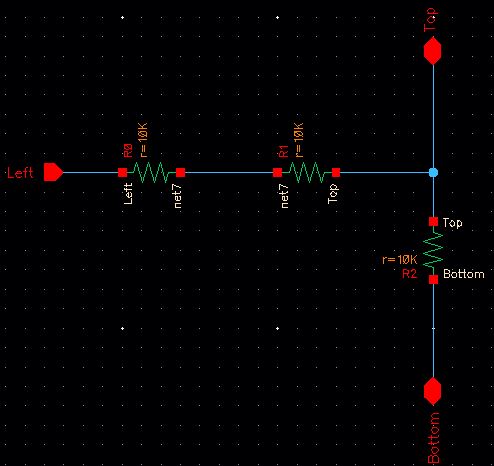
In this lab, we will further develop the 10-bit DAC/2R_Res from Lab #2 by using the n-well to layout 10k resistors in accordance with the schematic below.
To start, create a new library in Cadence titled, Lab_3. From lab2 and/or Tutorial #1, copy the following cellviews to the Lab_3 library: 2R_Resistor & R_n_well_10k. If you have never created such cellviews, follow the steps found in Tutorial #1 and/or the Pre-lab to create a 10k resistor.
*How to select the width and length of the resistor by referencing the process information from MOSIS.- The sheet resistance of n-well in the C5 process is roughly 800 ohms.
- The
minimum width of the n-well is 12 lambda (3.6 microns since lambda here
is 300nm)
- Given these parameters we can use the following equation to determine the width and length to create a 10k resistor.
- Another parameter to consider is that a given length and width must be divisible by 0.15u in order to "snap to grid".
- To do so, we will use L = 56.1u and W = 4.5u. (Measurements can be verified in the pictures below)
In the 2R_Resistor cellview, create a new layout and instantiate three of the R_n_well_10k
resistors and stack them on top of each other like a ladder. As always,
there is a mimimum amount of spacing required in between the resistors,
so keep that in mind and DRC after placing the three resistors to
ensure they meet the proper standards.
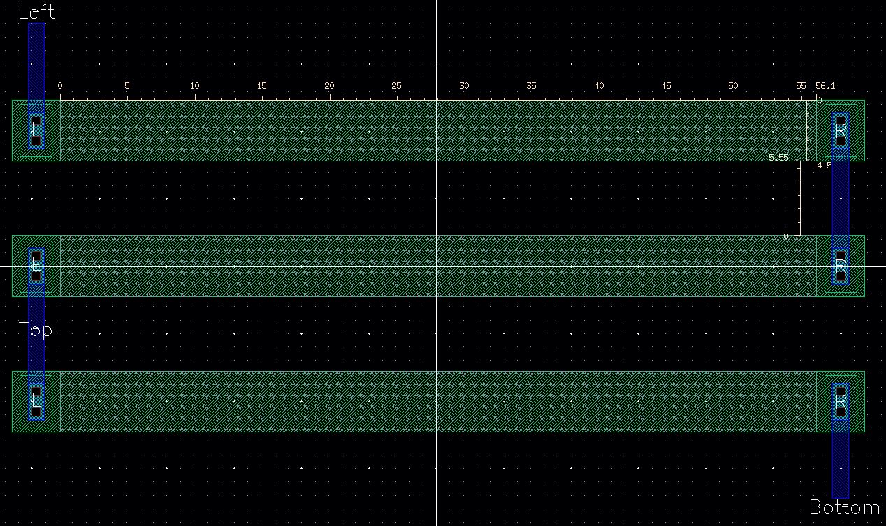
Link all the resistors by drawing rectangles in the metal1
layer from one resistor to the next following the picture above. In the
same metal1 layer, create pins (Top, Bottom, Left) and place them
accordingly. In doing so, we ensure that we are following the schematic
drawn above for the 10-bit DAC.
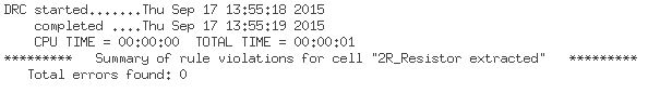
DRC the layout to ensure it continues to meet stardards.
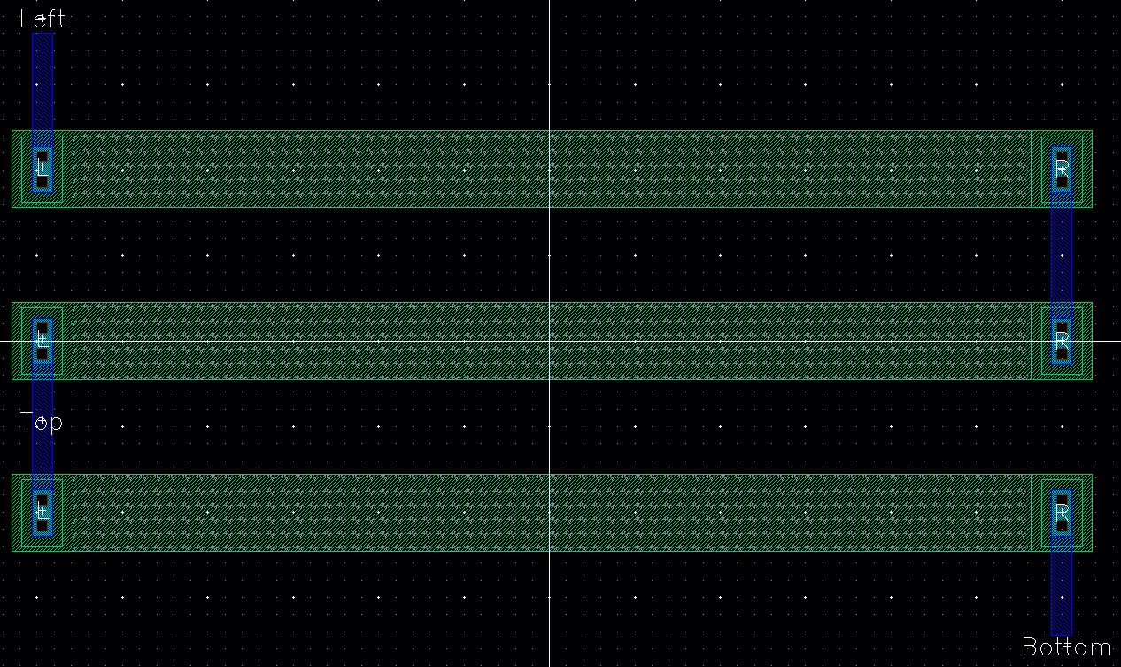
Once DRC is completed, extract the layout and open it. It should look similar to the one displayed below.
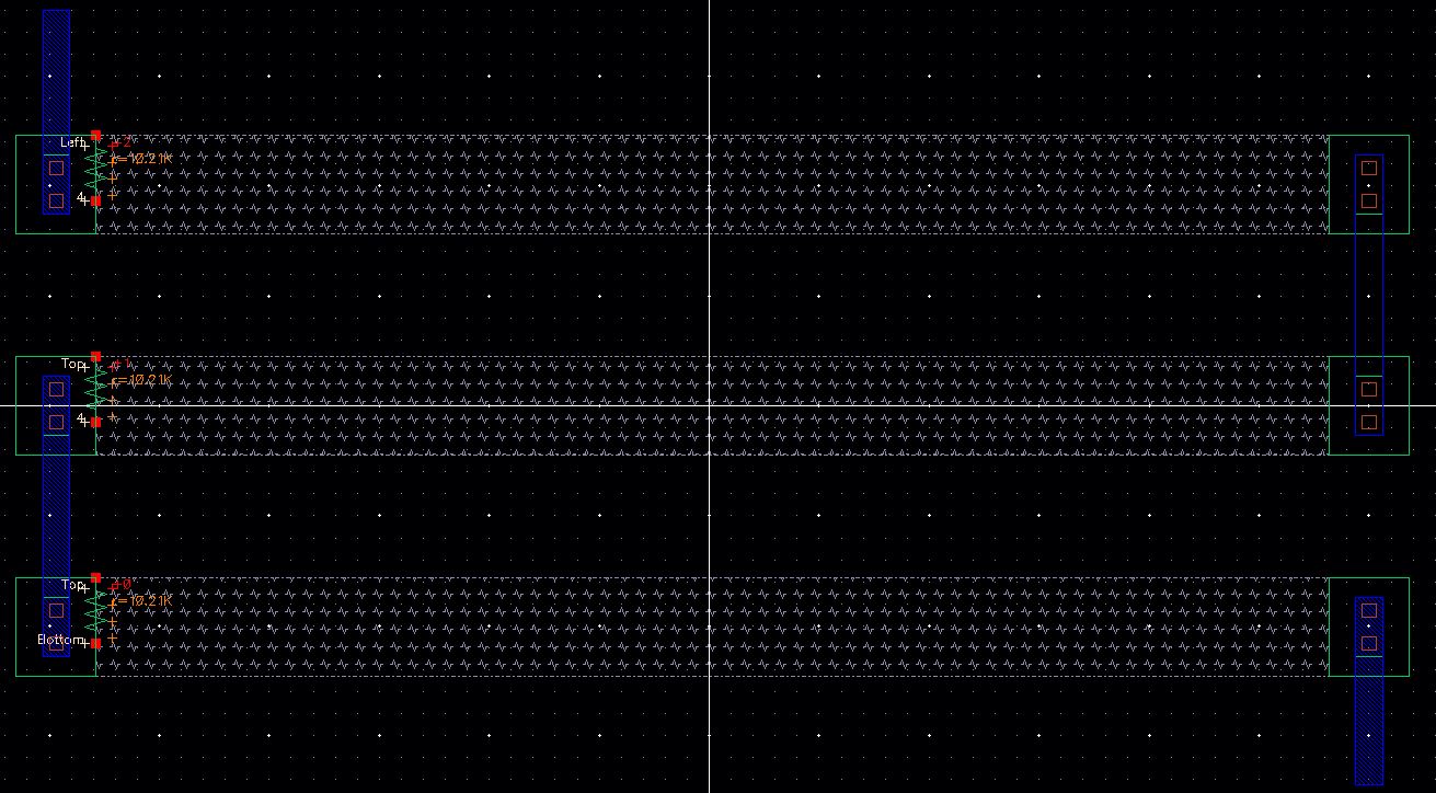
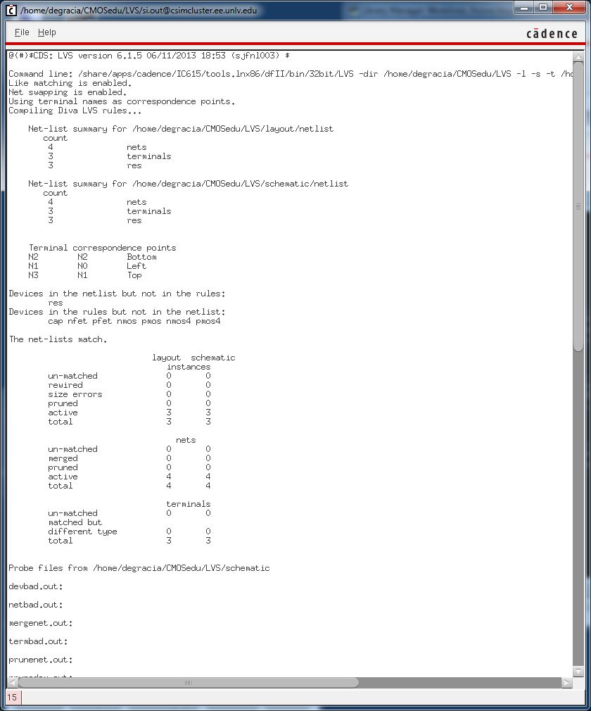
DRC and LVS the extracted layout to compare it to the original schematic.
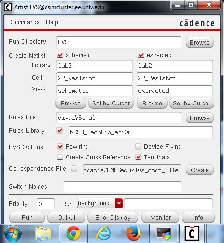
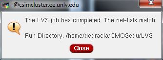
This helps us check if the netlists match and there are no issues.
One can also click Output on the Artist LVS window to see what has occured.
Back up files
Afterwards,
it is always important to backup files by either creating a folder on
your personal computer, emailing the files to yourself and/or backing
it up on a cloud (dropbox, icloud, google drive).

Return to my labs
Return to EE421L Labs