
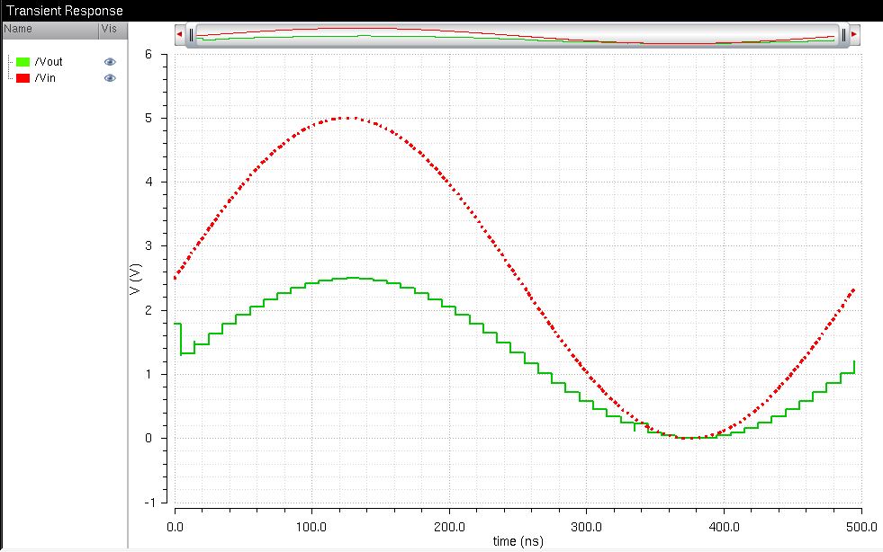
- An understanding of how the input voltage, Vin, is related to B[9:0] and Vout.
- An understanding of the ADC and DAC; analysis of simulations.
-
Explain how to determine the least significant bit (LSB, the minimum
voltage change on the ADC's input to see a change in the digital code
B[9:0]) of the converter.
2. Download the lab2.zip and unzip it in into the CMOSedu design directory. In addition, add the statement, "DEFINE lab2 $HOME/CMOSedu/lab2", into the cds.lib library.
3. Start Cadence and choose the following files as shown below.

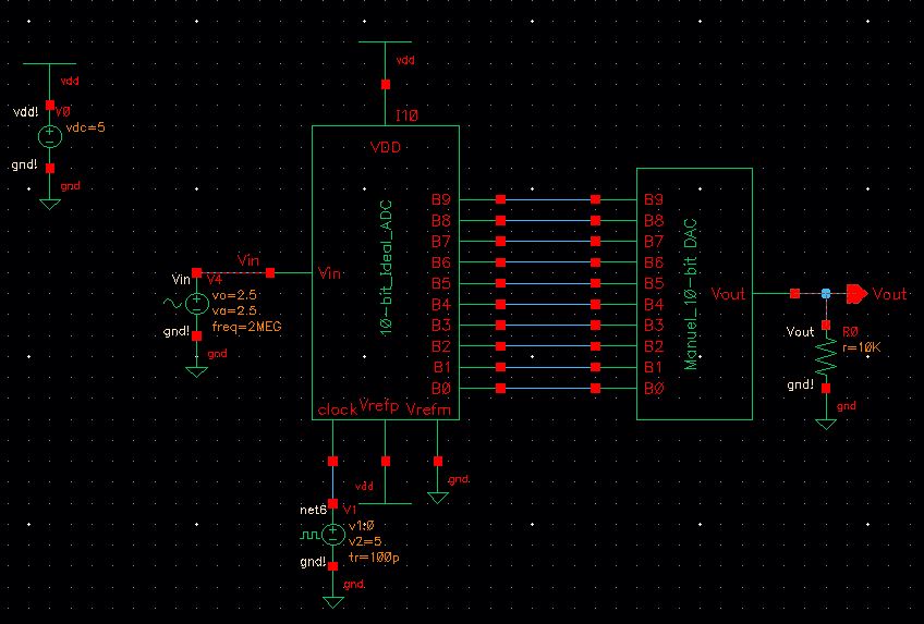
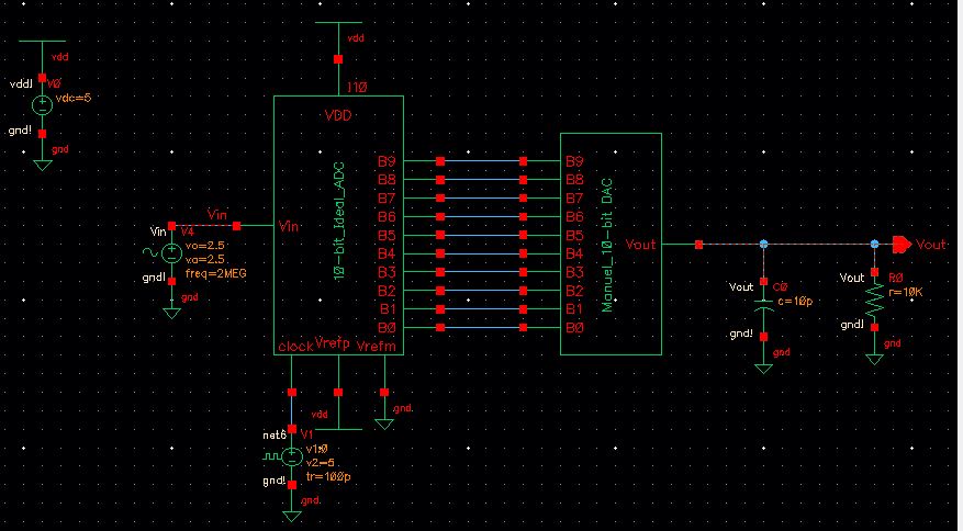
4. The following screen will appear displaying a 10-bit ADC to DAC Converter schematic.


7.
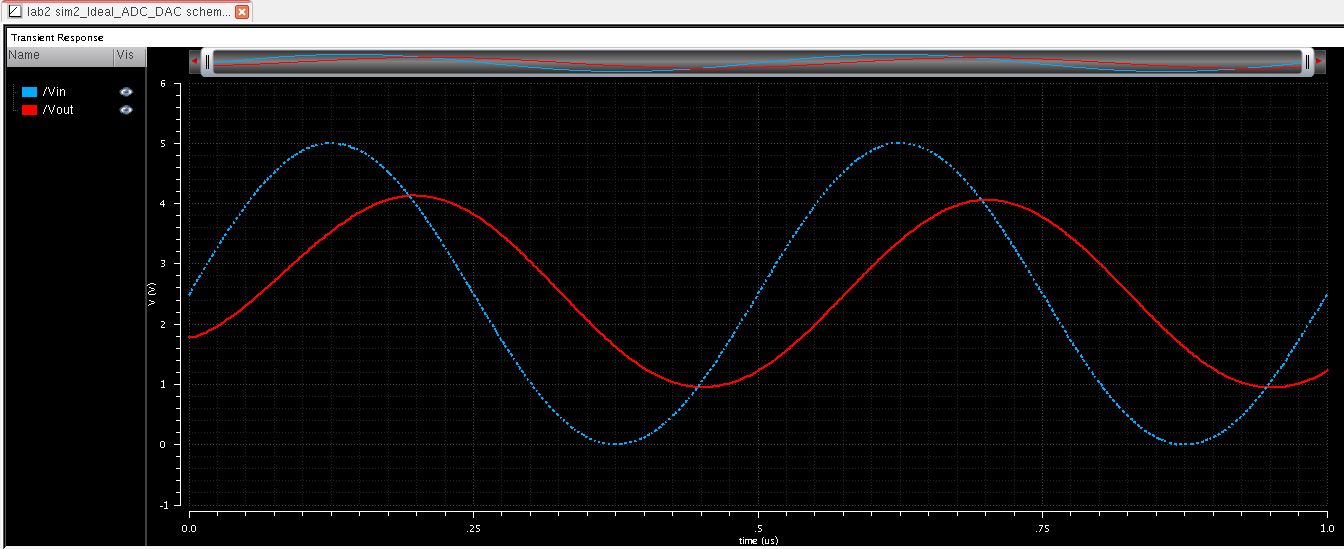
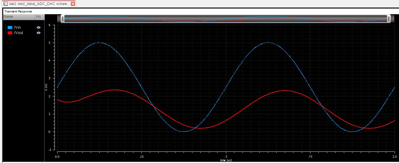
By changing the value of the offset voltage from 2.5V to 7.5V,
one can see through the analysis that the output voltage gets clipped
after a certain point due to reaching its limitations from 0V to 5V.

An ADC is an electronic process in which a continuosly variable analog signal is changed, without altering its content, into a multilevel digital signal.
Digital-to-Analog Conversion (DAC)
A DAC is an electron process that converts digital data into an analog signal, such as current and voltage. DAC is needed to be able to transmit, store, and manipulate data without any degradation or distortion.
Least Significant Bit (LSB)
The LSB can be described as the smallest level than an ADC can convert or the smallest increment a DAC outputs. It can be defined by the following:

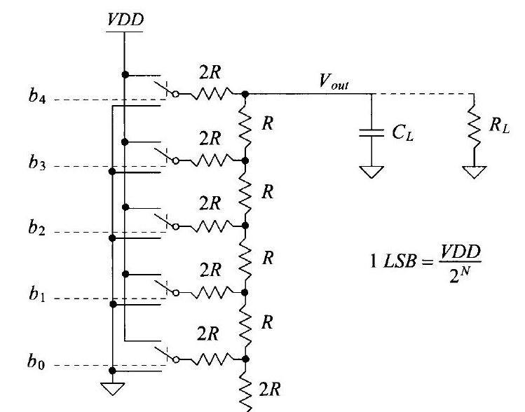
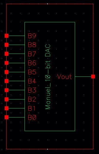
The design of a 10-bit DAC using an n-well R of 10k
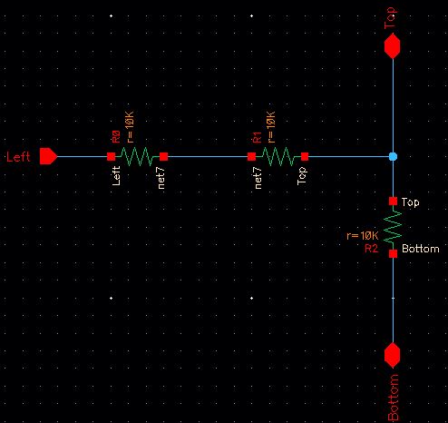
We start by creating a cellview (schematic) entitled, "2R_Res" in the lab2 folder. Then, build an individual DAC bit using 10k resistors as seen above. The design follows the appropriate ratio between 2R and R.
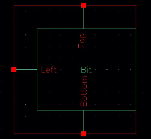
Afterwards, we then create a symbol to represent the schematic making sure that the pins are named and positioned properly (top,left, bottom). In doing so, we can use it later to build our 10-bit DAC.
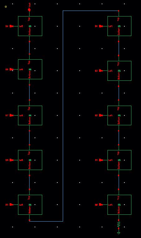
Given our newly created symbol, create a copy of the Ideal_10-bit_DAC labeling it, Mydesign_10-bit_DAC and delete everything inside. We will then use the symbol we just created to build our specialized 10-bit DAC as displayed below. In addition, do not forget to add the extra 10k resistor on the last bit to follow through with the topology given above. The left pin should be connected to the ADC bits, the first bit's (B9) top connected to Vout, and the last bit's (B0) bottom connected toground. Once created, check and save to make sure there are no errors found in the schematic.
Lastly, go back into the library manager and edit the symbol of the Mydesign_10-bit_DAC deleting VDD, Vrefm and Vrefp because they are not needed for our design. The symbol should mimic the one below.
Design Check
Create a copy of sim_Ideal_ADC_DAC entitled, sim2_Ideal_ADC_DAC which will be used for further design and analysis. As a safety measure to help in later troubleshooting, we can implement and simulate the Mydesign_10-bit_DAC in the sim2_Ideal_ADC_DAC to see if it runs properly.
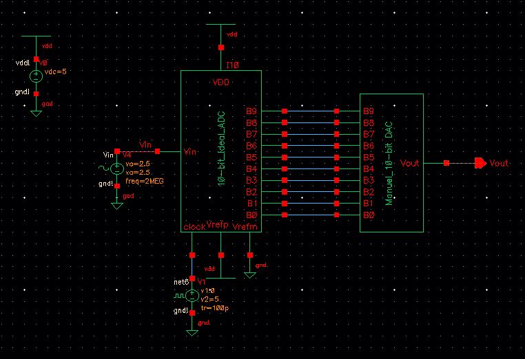
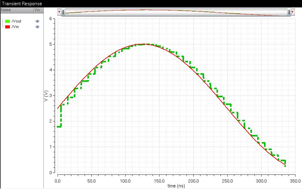
When
comparing the two simulations, one from the prelab and the other above,
we can see that they are very similar. Therefore, we can deduce
that Mydesign_10-bit_DAC is working properly.
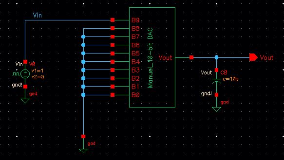
How to determine the output resistance of the DAC
To determine the output resistance of the DAC we first connect a 5V pulse to the B9 pin and ground B0 - B8. We then use the given equation found in the topology image to determine the LSB. The purpose of the Least Significant Bit (LSB) is to calculate the minimum voltage change by multiplying it with the appropriate binary number to get a value of 2.5V.
Delay, driving a load
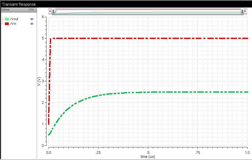
As stated earlier ground all DAC inputs except for B9 and predict the time delay by using the equation td = 0.7RC. Calculations are as followed [td = 0.7(10k)(10p) = 70ns]. The schematic and transient response is displayed below.
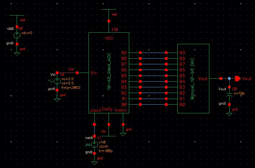
Simulations to show what happens if the designed DAC drives a load (R, C, and parallel R/C)
10k Resistor Load:
10pF Capacitor Load:
Parallel 10k Resistor and 10pF Capacitor Load:
Back up files
Afterwards, it is always important to backup files by either creating a folder on your personal computer, emailing the files to yourself and/or backing it up on a cloud (dropbox, icloud, google drive).