EE 421L - Lab 4 - IV Characteristicsand Layout of NMOS and PMOS Devices in ON's C5 Process

Jonathan K DeBoy
deboyj@unlv.nevada.edu
12 September 2015
Lab Files


Pre-lab work


Introduction

This lab we simulate the current verus voltage characteristics of both an NMOS and PMOS transistor from ON Semiconductor's C5 0.6ami process. We will simulate the drain current of different VGS' by sweeping the VDS on an NMOS. Then we will plot the drain current of a single VDS=100mV and sweeping VGS. The same operations will be performed for the PMOS, except they will involve the variables VSG and VSD. The layout for a PMOS of W=12u and L=600n and for an NMOS of W=6u and L=600n will be created, DRC'd, and LVS'd.


Probe Pad

Probe pads are useful for creating a signal test point on a chip for verification purposes. Below is the layout, schematic, symbol, and DRC verification of one.             Probepad Schem Probesym
Probepadlayoutprobedrc


NMOS ID vs VDS Sweep with 6 Different VGS Plots

VDSschem
VDSsim


NMOS ID vs VGS Sweep with VDS=100mV

 
VGSschem
VGSsim


PMOS ID vs VSD Sweep with 6 Different VSD Plots 

VSDschem
VSDsim


PMOS ID vs VSG Sweep with VSD=100mV 

VSGschem
VSGsim


NMOS Layout 


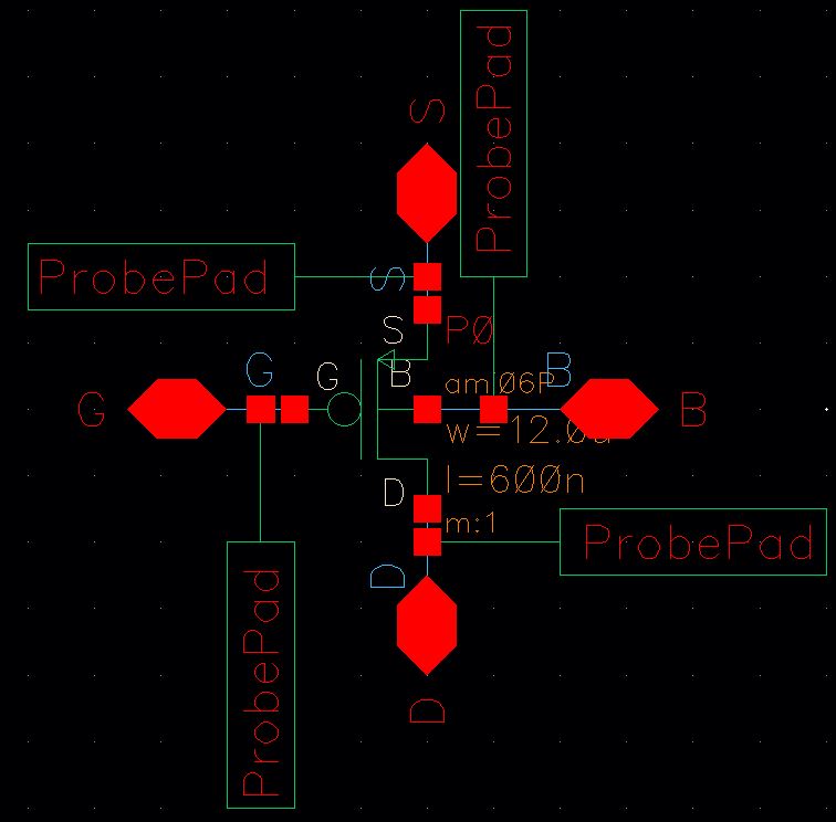
Schematic of a 4 terminal NMOS with probe pads.

Layout of a 4 terminal NMOS with probe pads

Zoomed in layout on the NMOS

Verifications

PMOS Layout 


Schematic of a 4 terminal PMOS with probe pads.

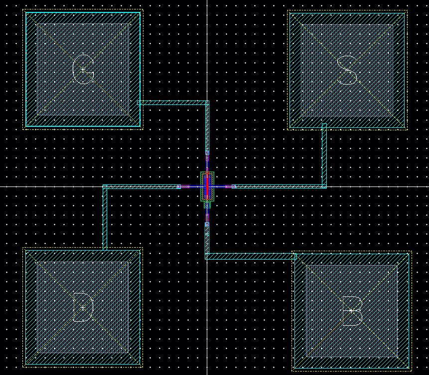
Layout of a 4 terminal PMOS with probe pads

Zoomed in layout on the NMOS

Verifications


Return
Return to EE421L Student Directory
Return to EE421L Page
Return to CMOSedu