This
lab we make the layout of the 10-bit digital to analog converter we
designed last time. The entire layout will be made of 10k n-well
resistors.
Resistor Design
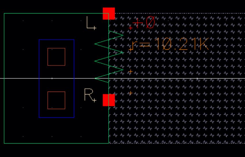
Luckily our design only requires
one unique component: a 10k n-well resistor. For starters, we make the
layout for a single resistor by selecting our lengths and widths to be
a multiple of the scale factor: 300nm. To get 10k ohms, we need to
determine how many sheets are needed (800 ohms per nxn square). With a
minimum width of 3.6um, lets choose 4.5um which is 15 squares wide. At
800 ohms per square and a desire of 10k, we can determine that we need
187.5 block long. This is not a whole number so we need to round up a
little and end up with 10.1k instead of exactly 10 to make the design
rules.
To measure the lengths and widths, place a
rectangle of the n-well layer on a new layout, select it and press q.
Then choose the left and right fields to be half of the total length
(one positive and one negative). Do the same for height. For ease of
mind, press k and insert a ruler to actually measure the size of the
resistor.
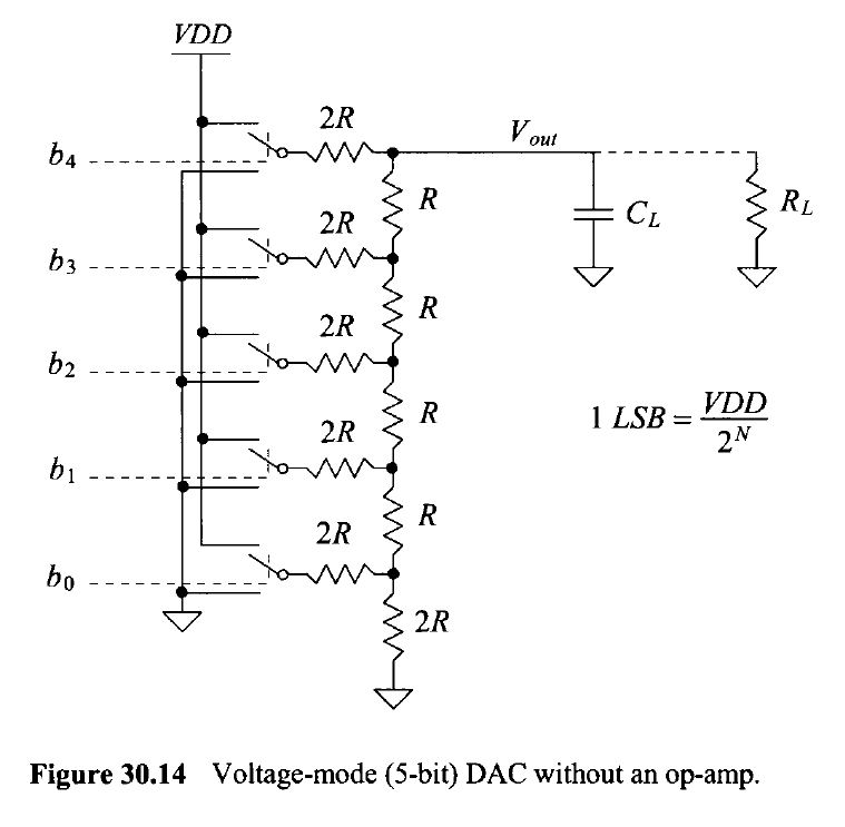
10-Bit DAC Layout
Below is the
schematic and output
resistance derivation of our simple resistor DAC (ours is extended for 10 bits).
Below is the laout for a single DAC block. This is be instanced 10 times in a higher level.
Even though this
design may seem cooler, notice how the lengths of metal between a
select few bits are much longer than others, causing a non-linear delay
for an entire conversion. The dealys seen on this layout are much
longer than if all the DAC bits were placed adjacent to each other. In
fact, this layout takes up more area than the latter, however it is
more condensed into a rectangle rather than a line.
This is the final layout used for the DAC, side by side bits.
Above
is the Design Rule Check (DRC) and Layout vs Schematic (LVS) forms of
verification to show that our layout above meets the rules of
OnSemiconductors' C5 process and matches with our schematic below. The
verification on the left is for the DAC and the one on the right is for
the DAC bit block.