Lab
X - ECE 421L
Authored
by Worku, Yetneberk
Email: workuy@unlv.nevada.edu
NHSE ID 1007208058
09/29/2014
Pre-lab Three
First,Back-up all of your work from the lab and the course, then finish Tutorial 1
Post-Lab
This
lab will focus on the layout of the 10-bit DAC, that use Tutorial 1 to
help create a loyout for the DAC bit created in lab2.
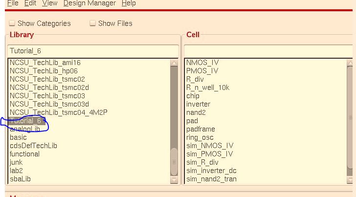
First, create new liberary call Lab3, and download the zip file from tutorial_6.zip
file. after download and unzip the file, then need to define and add in
location cds.lib. then, will get liberary manager as follows.
Next,
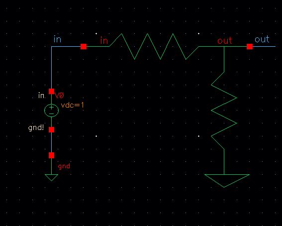
we can use the symbol of diveder, that we used in lab1. except the in
and out pin delate everthing. first, draw the symbol, second, add wire,
wire names, input voltage 1V, when we finished check and save the
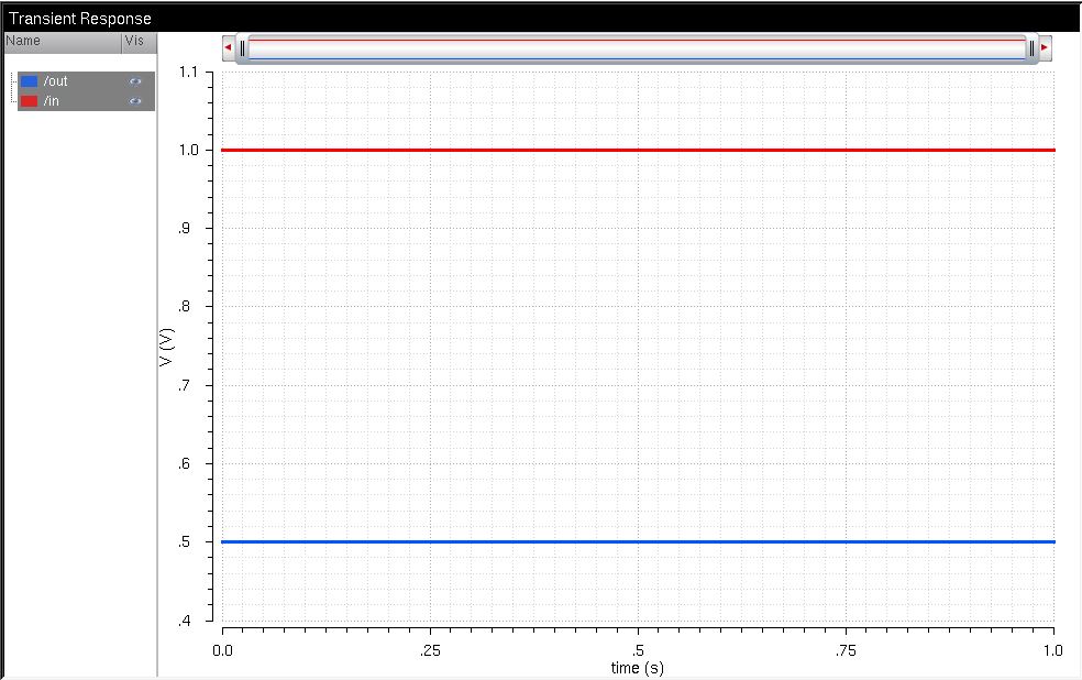
schematic. then draw figure, transient response and with the input
voltage, showing below.

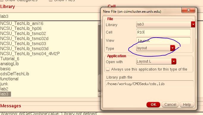
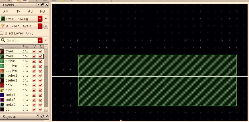
Now, create new layout in lab3; that to begin laying out a 10k resistor that showing below.
Next, by chosing the n-well, and create rectangle mode, then the image should be look like one below.
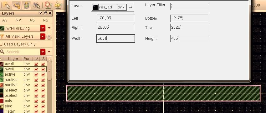
Next,
creating 10k resistors, need to follow the design rules that is the
sheet resistace is approximatlely 800ohms, minimum width of 12λ, minimum spacing of wells at different potential of 6λ, and mimimum spacing of wells at different potential of 18λ. however, L/W= 12.5 so the minimum width can be W= 3.6um, so by selecting W= 4.5um, then L= 56.1, now, i know all this dimensions fall on grid. that showing fig below.
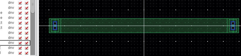
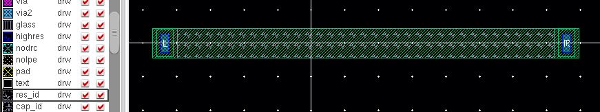
Next, adding ntaps on each side the n-well the image should be look like one below.
Next,
creat the pin by selecting metal1, then place on the right and the left
ntap, L and R respectively. that showing the image below
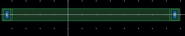
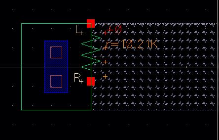
Next, select res_id, and use the rectangle tool then highlight the body of the resistor, the image should be as follows.
Next, by doing verify and extract, we will get the value of the resistor. R=10.21k
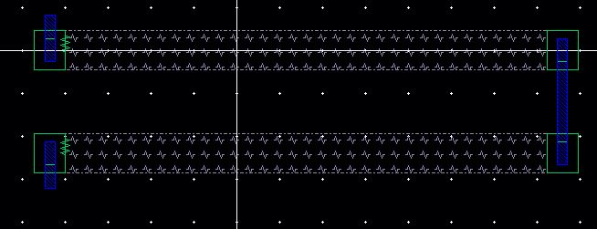
Next,
by doing two of the 10k n-well resistor layouts, that DRC of layout to
ensure the resistors are far enough apart. the design
rules say that they are 18 lambda away from each other. first, select
the melal1 layer, add rectangles to connect resistor together, and pins
of resistors. second extract a view from our R2R layout the image
should be similar to below.
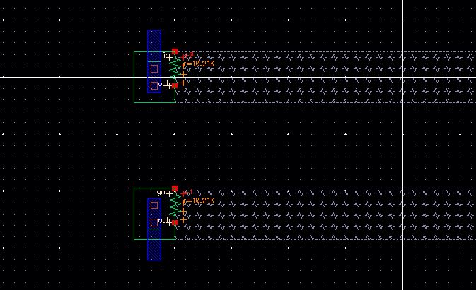
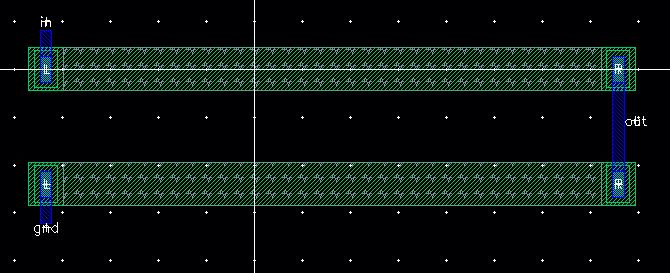
Finally,
first give error, then edit rectagle pin properties of the gnd, in, and
out; then save extract and LVS. there shouldn't be any errors.
the result of image showing below

now to back up the file dragging out lab3 from mobaterm to the sedktop ane e-mail to myself
the lab3 download is here
Return to the listing of my labs
Return to the whole class report
Return to the EE421L site
Return to the CMOSedu.com