Lab 6 - ECE 421L
Authored
by Leanna Guevara, guevaral@unlv.nevada.edu
October 20, 2014
Design, layout and simulation of a CMOS NAND gate, XOR gate and Full Adder
We will be using Tutorial_4 for the completion of the lab. The tutorial goes over how to create the schematic and layout of a 2 input NAND gate.
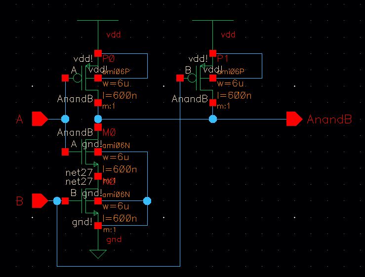
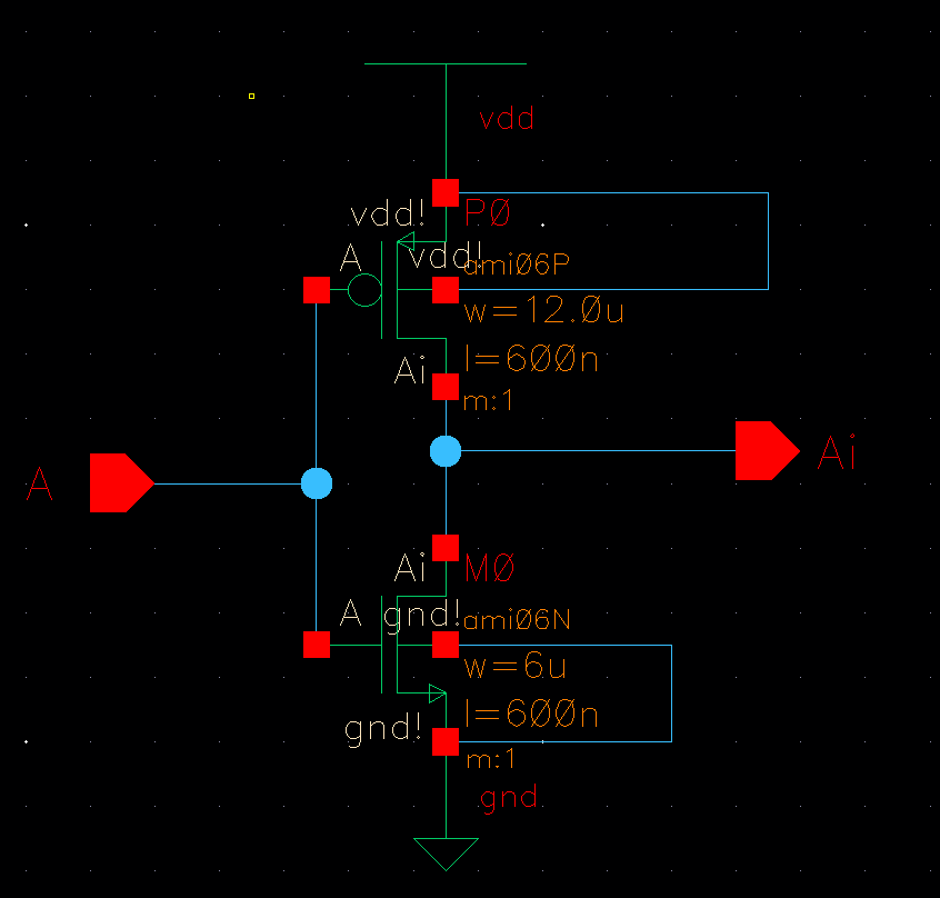
2-input NAND GateSchematic:
Creating the schematic should a simple process if we have been copying the libraries from previous tutorials and labs. Create a new cell and use the inverter cell created from lab 5, this will allow us to copy the nmos and pmos symbols already in place.
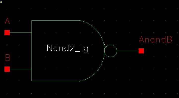
Symbol:
Once the schematic has been checked and saved with no errors we can create the symbol (Create->Cell view->From Cell view). Make sure the inputs and output pins are in the correct location by displaying them (q->display value)
Layout:
Copy the inverter layout from lab 5 to make life easier, we can copy the parts available instead of searching for them again.
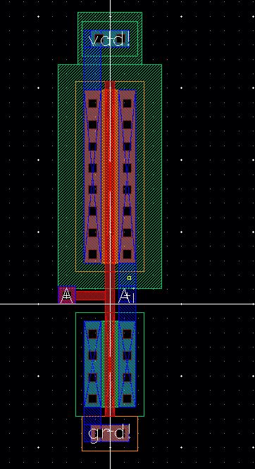
Because
there are two inputs this time we need a second nmos and pmos. Copy the
pmos and nmos (Select->C->Drag to desired location) and align one
set of contacts so it just looks like a giant nmos or pmos. We do not
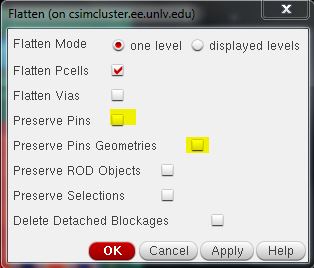
need the metal in between the two MOSFETS, there fore we can flatten them in order to seperate the parts (Select both MOSFETS->Edit->Hierarchy->flatten)
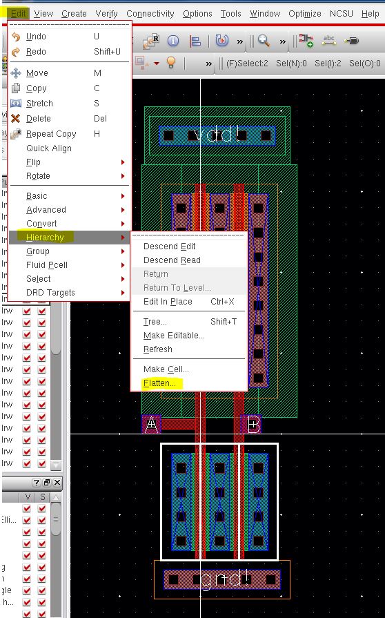
After clicking flatten the following window appears, make sure to deselect the box for Preserved Pins and Preserved Pins Geometries.
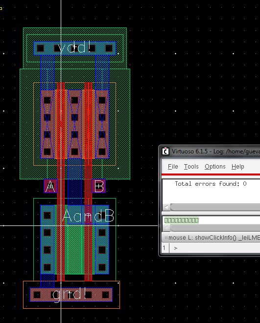
The final layout should look like the following
Notes
- Change the ntap and ptap to 5 columns instead of 2
- Although
we are copying the inverter to previous labs make sure that the width
and length are simliar to the current schematic we are recreating.
Change the width of the pmos from 12u to 6u.
- DRC the layout to ensure that we are following the rules and that there are no errors.
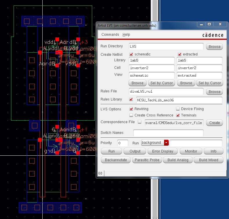
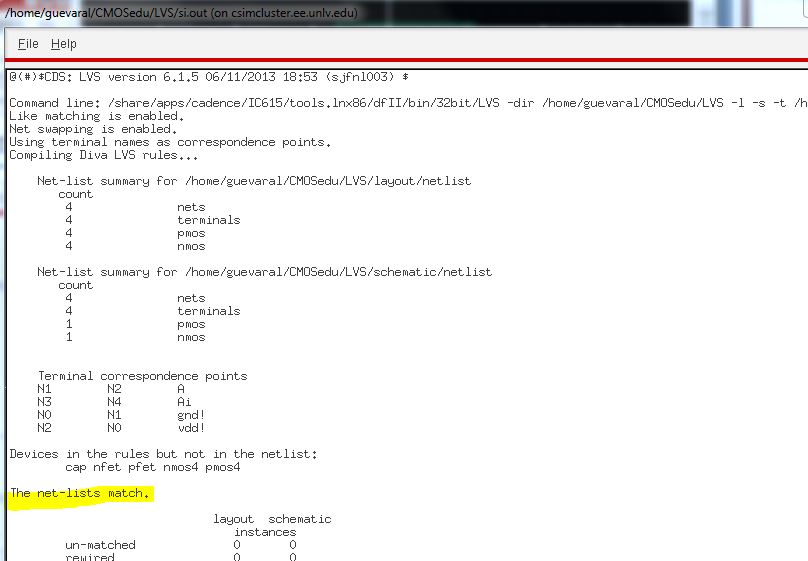
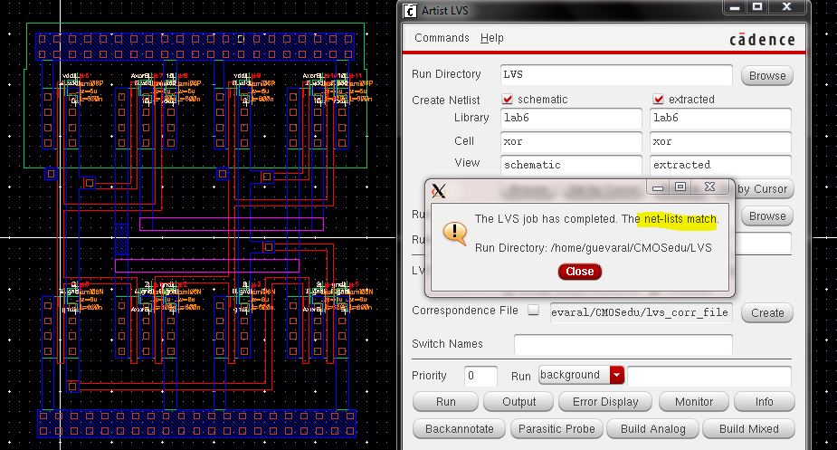
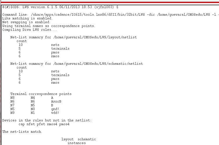
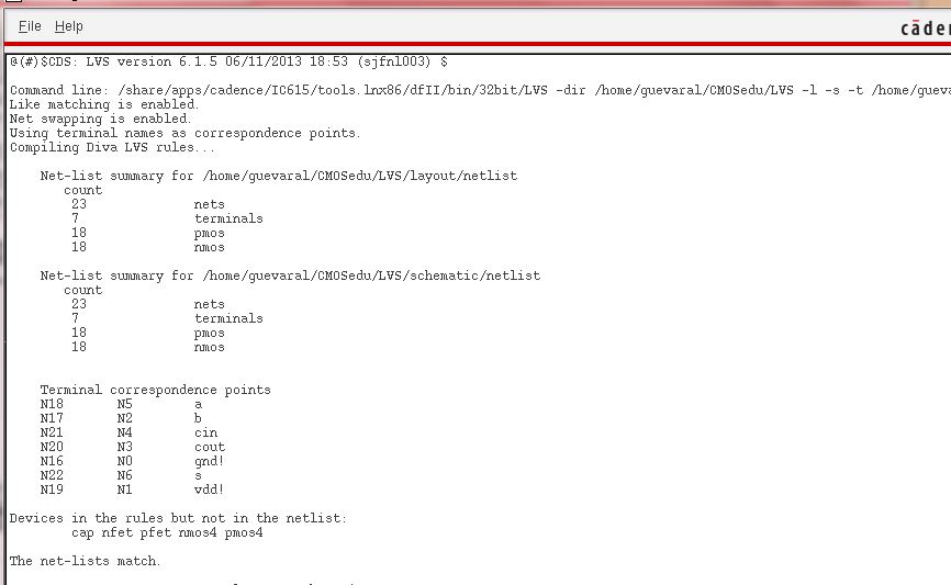
- Extract the layout so we can LVS the systems and ensure that the netlist match.
LVS
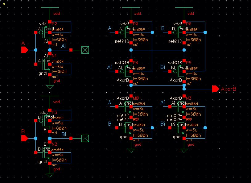
2-Input XOR Gate
Schematic
Just like NAND gate its best to just copy the cells to save time.
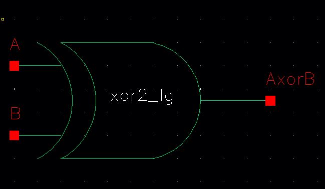
Symbol:
Layout:
This
is where the lab gets confusing, I copied the inverter cell and copied
the how everything was placed to get an understanding of the layout.
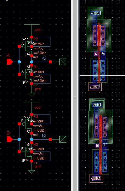
Becareful
when crossing and connecting layers. It took a while to correctly
connect everything, the final layout should look like
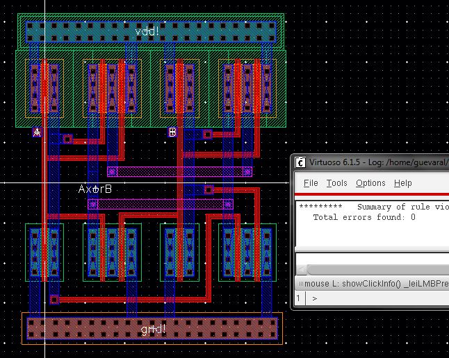
LVS:
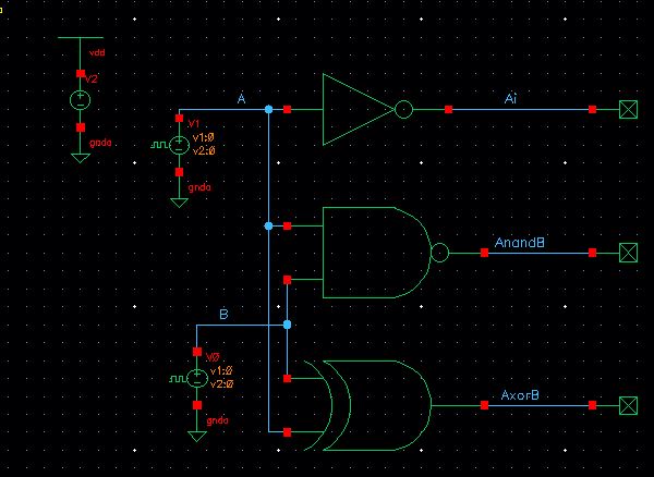
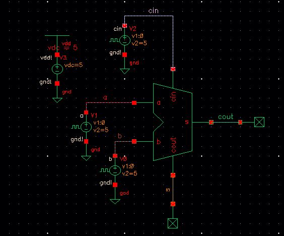
To test the gates (NAND, XOR, and INVERTED) are working properly we will run a simulation
Schematic:
Simulation:
The pulse for input A and B are differnerent, variation in the pulse completely changes the simulation results.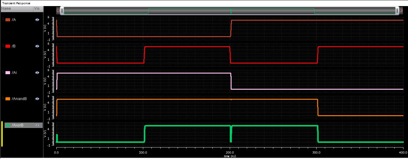
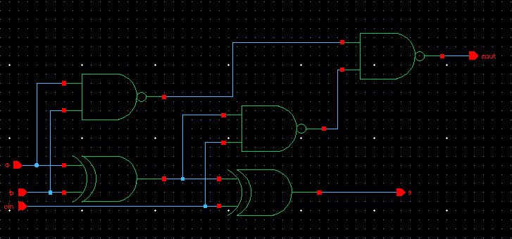
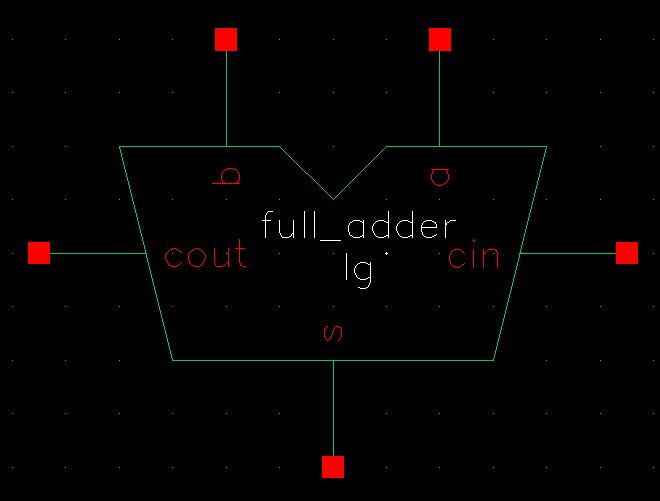
Full-Adder
Schematic:
Symbol:
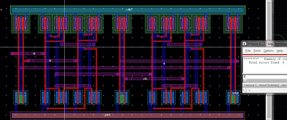
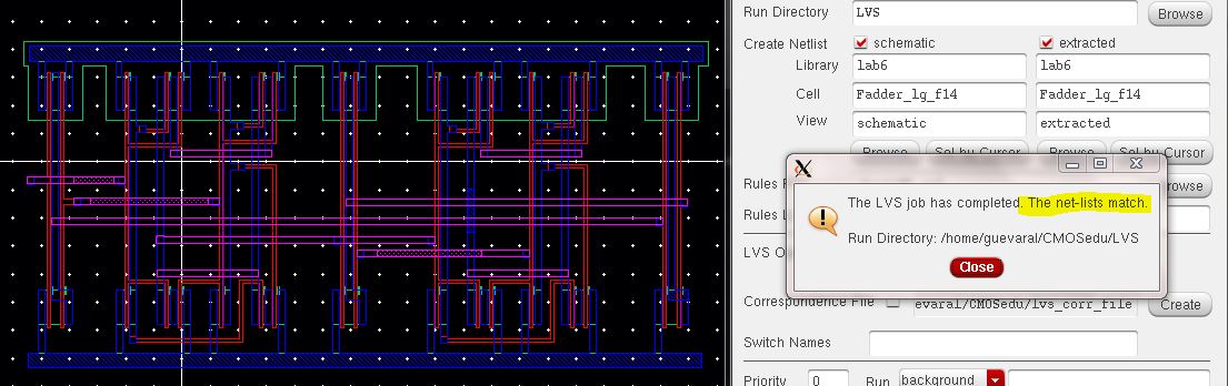
Layout:
Because
there are many components and its easy to get lost I layed out the nand
and xor gates similiar to the order in the schematic.
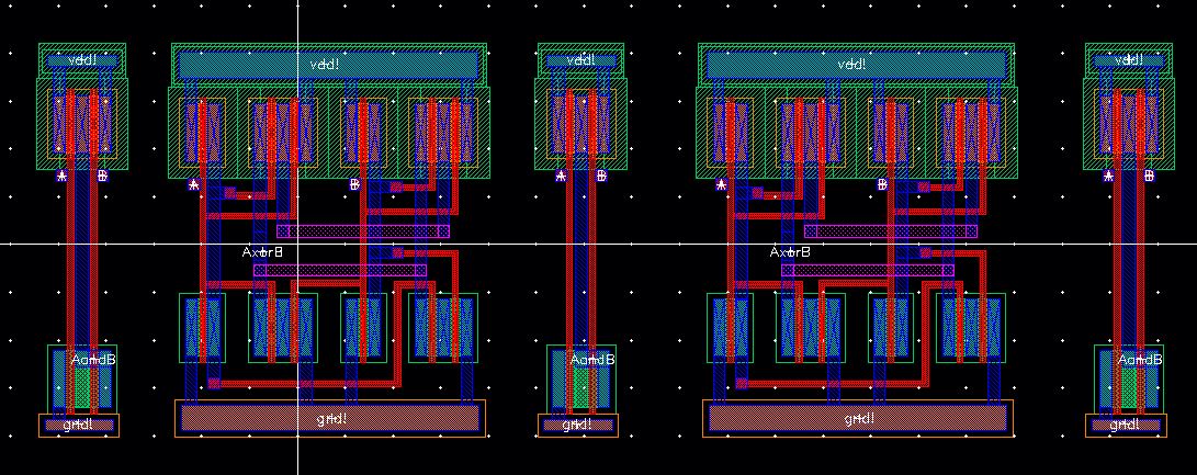
The next step is to connect the inputs and outputs. Make sure to DRC the layout to ensure the rules are being followed.
LVS:
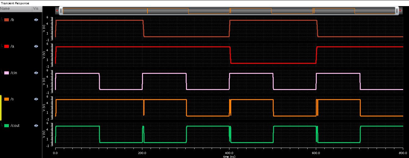
Simulation:
This concludes Lab 6.
Remember to download and email the file to yourself for safe keeping.

Return to EE 421 Labs