Lab 3 - ECE 421L 

Authored by Leanna Guevara,

guevaral@unlv.nevada.edu

September 29, 2014 


Layout of a 10-bit digital-to-analog converter (DAC)


For this lab we will be recreating the 10 bit DAC from lab 2 using the layout techniques learned in Cadence Design System Tutorial 1.

http://cmosedu.com/jbaker/courses/ee421L/f14/students/guevaral/Lab%202/2R_Res_Schematic.JPG


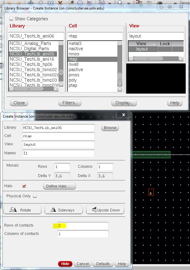
First the 10k resistor layout needs to be created by following the steps in Tutorial 1. 

http://cmosedu.com/jbaker/courses/ee421L/f14/students/guevaral/Lab%203/Tutorial1.1.JPG

We 
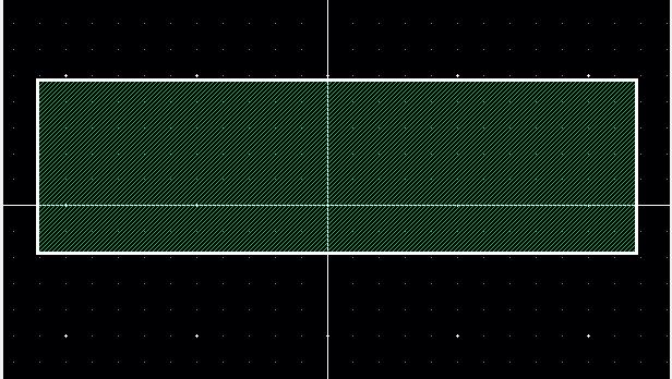
can edit the length and width of the rectangle by clicking rectangle 
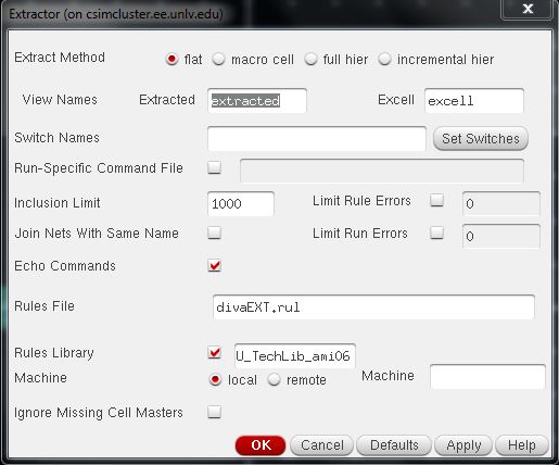
and pressing "q" (object). The following window should appear.

http://cmosedu.com/jbaker/courses/ee421L/f14/students/guevaral/Lab%203/Tutorial1.2.JPG

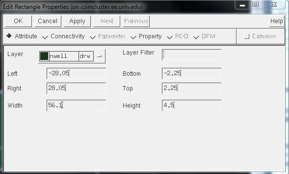
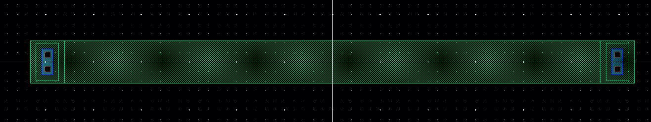
From the Edit Rectangle Properties window we can not only change the size of the rectangle but also the layer type. Based on the tutorial we make the width 56.1 um and height 4.5 um.  Instead of typing the measurements directly on the width and length box we use the left, right, bottom, and top boxes in order to have the rectangle at the center (this will help when dealing with multiple layers in other labs). Once the meansurements have been entered press OK.


Make sure to design rule check (DRC) before continuing to ensure that there are no errors.

In order to connect the resistor to other object we must insert ntap to both ends.
http://cmosedu.com/jbaker/courses/ee421L/f14/students/guevaral/Lab%203/Tutorial1.3.JPG
   
At first the ntap is just a red box to change the look press "e" for Display options and stop the display level at 10.    

http://cmosedu.com/jbaker/courses/ee421L/f14/students/guevaral/Lab%203/Tutorial1.4.JPG


After the adjustment the resistor should look like this (Don't forget to DRC afterwards) to make sure there are no errors.

http://cmosedu.com/jbaker/courses/ee421L/f14/students/guevaral/Lab%203/Tutorial1.5.JPG


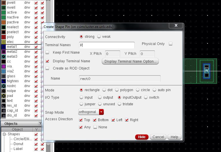
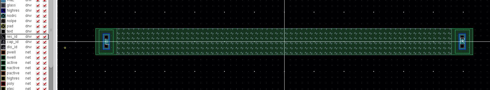
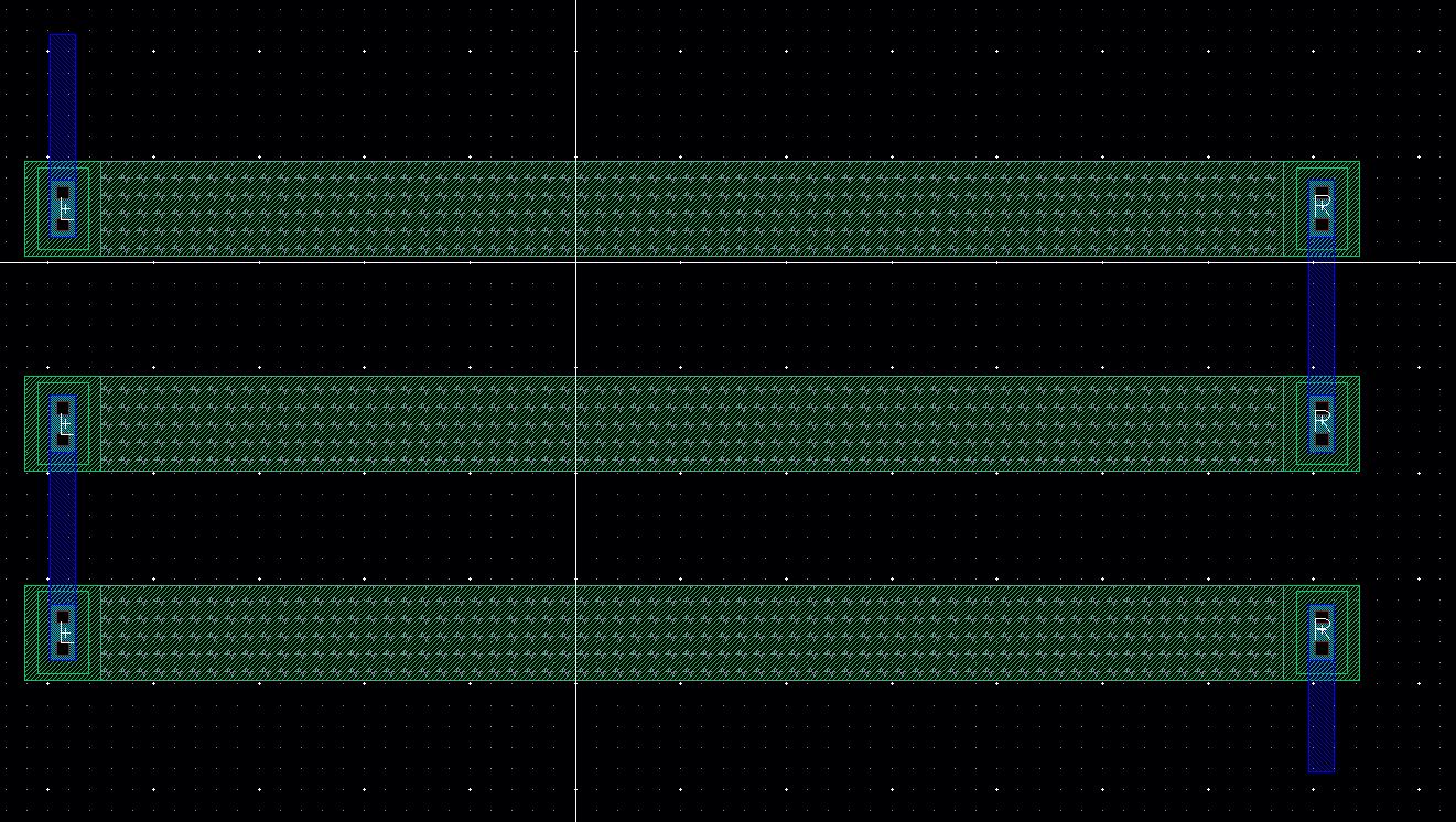
To add pins to the layout go Create ->Pin. We will label "L" for the left pin and "R" for the right pin. Make sure to select Display Terminal Name. Use the Metal 1 layer to draw the box around the ntap and make sure the lable is  placed in the middle of the box.

http://cmosedu.com/jbaker/courses/ee421L/f14/students/guevaral/Lab%203/Tutorial1.6.JPG


To identify the resistor select the res_id layer and draw a rectangle (select "r") around the resistor.

http://cmosedu.com/jbaker/courses/ee421L/f14/students/guevaral/Lab%203/Tutorial1.7.JPG

   
Extract the layout to determine the resistor value
http://cmosedu.com/jbaker/courses/ee421L/f14/students/guevaral/Lab%203/Tutorial1.8.JPG
   
An extracted view will  be placed in the cell group. When the extracted view is opened the follwoing should be shown..
http://cmosedu.com/jbaker/courses/ee421L/f14/students/guevaral/Lab%203/Tutorial1.9.JPG*
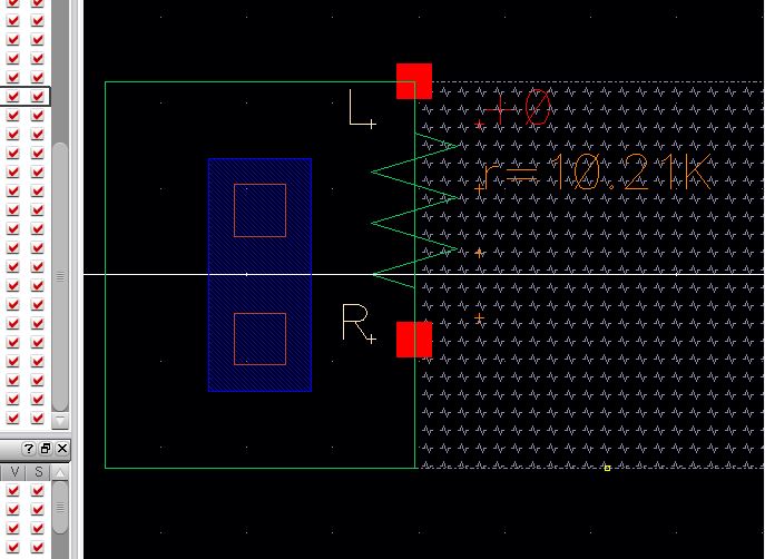
Note that he value is not exactly 10k ohms
   
Now that we have the resistor we can recreate the 10 bit DAC from lab 2. Remember to save the layout and close the layout and extracted windows.
       
Open a new layout window and place three of  the resistors we just created using instance. There is a minimum amount of spacing required in between the resistors so make sure to DRC the layout so ensure that the resistors meet the requirement.
http://cmosedu.com/jbaker/courses/ee421L/f14/students/guevaral/Lab%203/10bitdac.JPG   

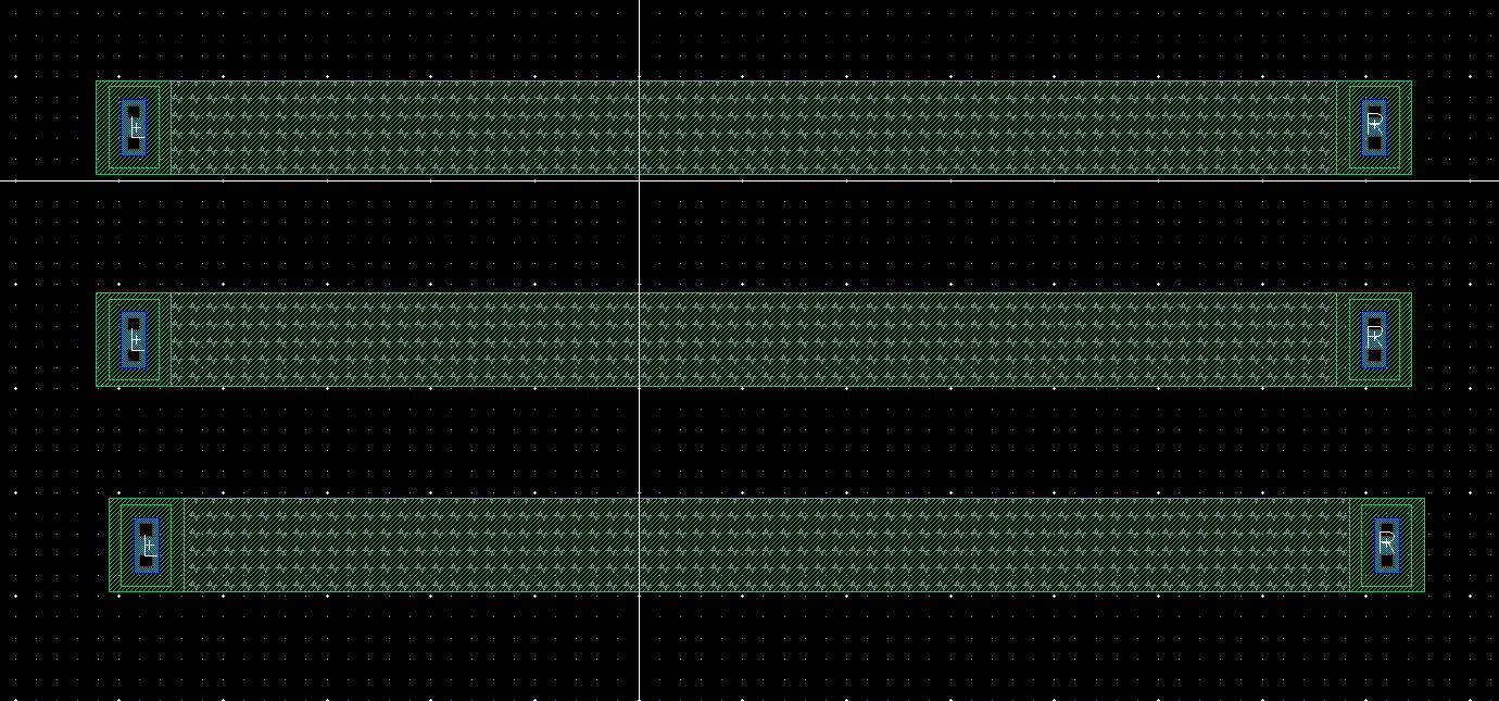
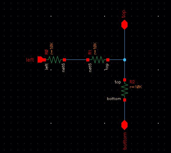
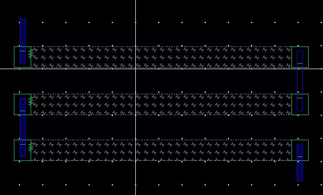
Link all three reistors by drawing Metal 1 rectangles. The layout should look like the following.

http://cmosedu.com/jbaker/courses/ee421L/f14/students/guevaral/Lab%203/10bitdac2.JPG


Noting the 10 bit DAC created in lab 2 we can see how the pins need to be placed. DRC the layout to ensure that there are no errors.


http://cmosedu.com/jbaker/courses/ee421L/f14/students/guevaral/Lab%203/10bitdac3.JPG


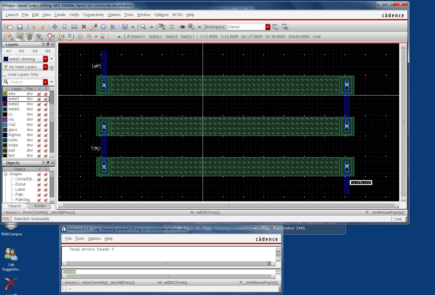
If there are no errors extract the layout.

http://cmosedu.com/jbaker/courses/ee421L/f14/students/guevaral/Lab%203/10bitdacExtract.JPG 


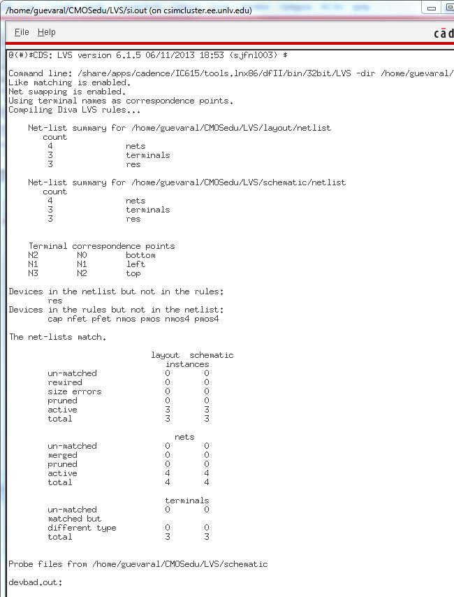
LVS the layout to compare the original schematic to the layout.

http://cmosedu.com/jbaker/courses/ee421L/f14/students/guevaral/Lab%203/10bitdacLVS.JPG


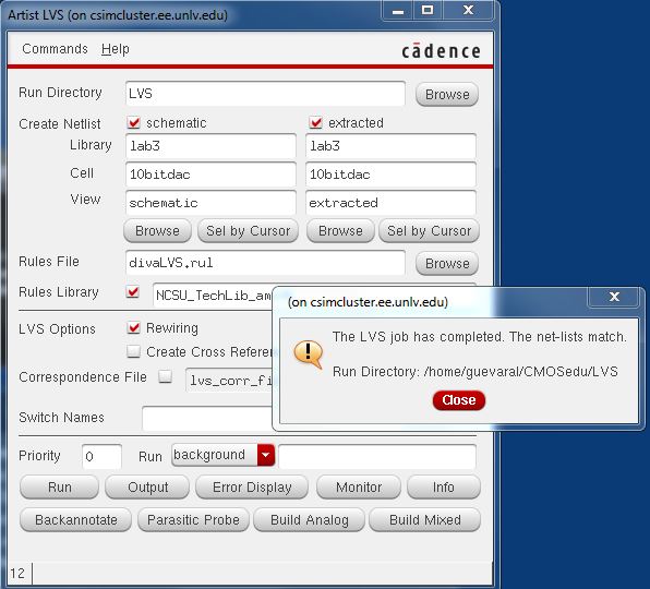
If you click Output on the Artist LVS window the following should appear


http://cmosedu.com/jbaker/courses/ee421L/f14/students/guevaral/Lab%203/10bitdacLVSout.JPG

   
This proves we have successfully created the same 10 bit DAC from lab 2. This concludes Lab 3


Remember to zip the lab 3 file from mobaXterm and email to yourself for safe keeping.

http://cmosedu.com/jbaker/courses/ee421L/f14/students/guevaral/Lab%203/zip.JPG


Return to EE 421 Labs