Lab 2 - ECE 421L
Authored
by Leanna Guevara, guevaral@unlv.nevada.edu
September 22, 2014
Design of a 10-bit digital-to-analog converter (DAC)
Pre-Lab
Download lab2.zip and to the CMOSedu directory. Don't forget to add the statement "DEFINE lab2 $HOME/CMOSedu/lab2" in the cds.lib. From here we can start Cadence.
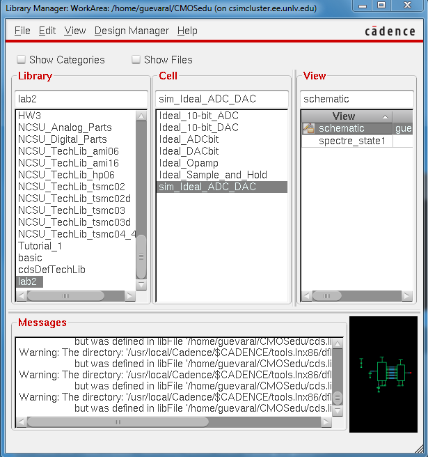
Go find the lab2 library and open the sim_Ideal_ADC_DAC schematic.
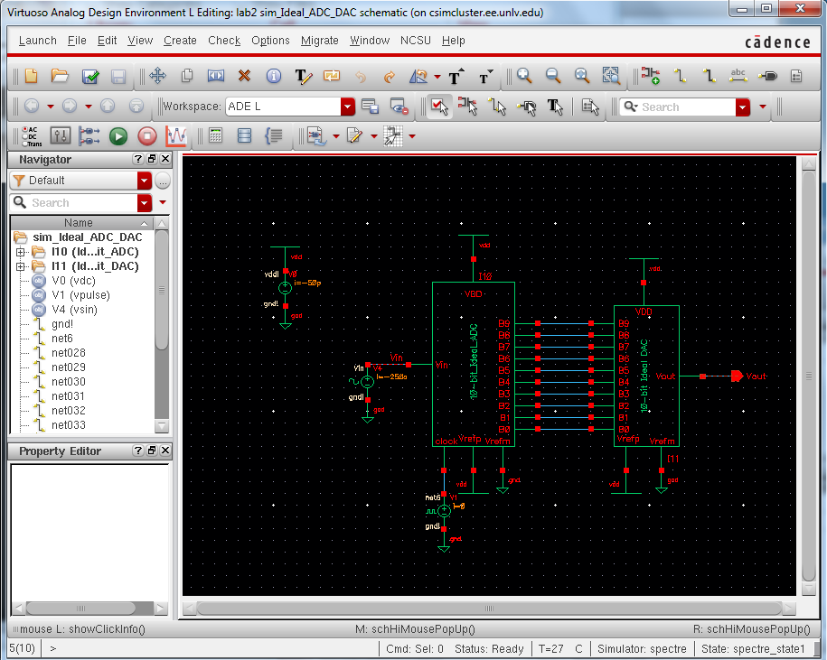
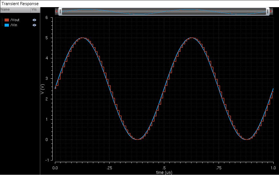
Run the simulation (Launch->ADE L->Session->Load State->Cellview->OK-> )
)
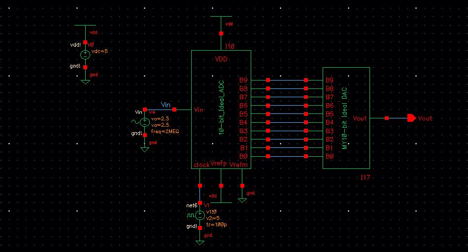
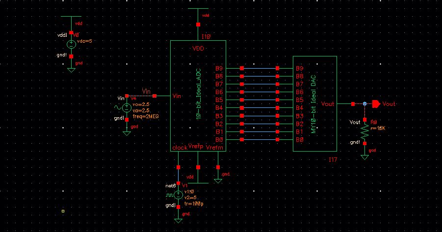
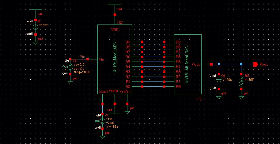
Post LabOur lab will be based on the following topology
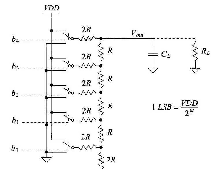
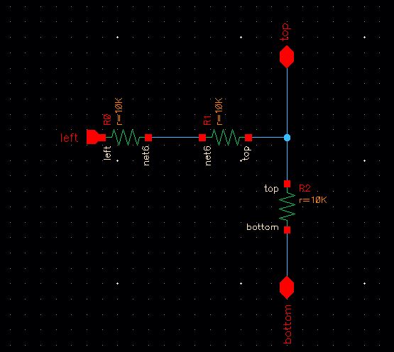
We will be creating a 10-bit DAC using n-well resistors.A resistor divider symbol needs to be created for the topology. From the library manager make a schematic called "2R_Res."
Once the schematic below is created make sure to check and save to make sure that there are no errors.
Creat
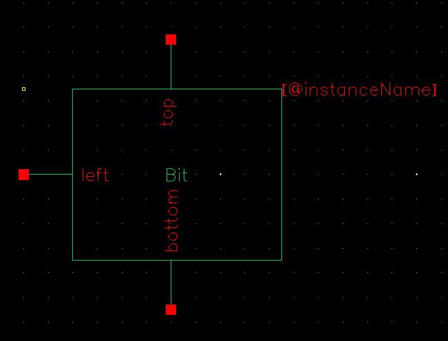
a symbol using the schematic (Create->Cellview->from Cellview).
The Symbol Generation Options should appear, make sure the left, top
and bottom pins are labeled then press OK. The following symbol should appear
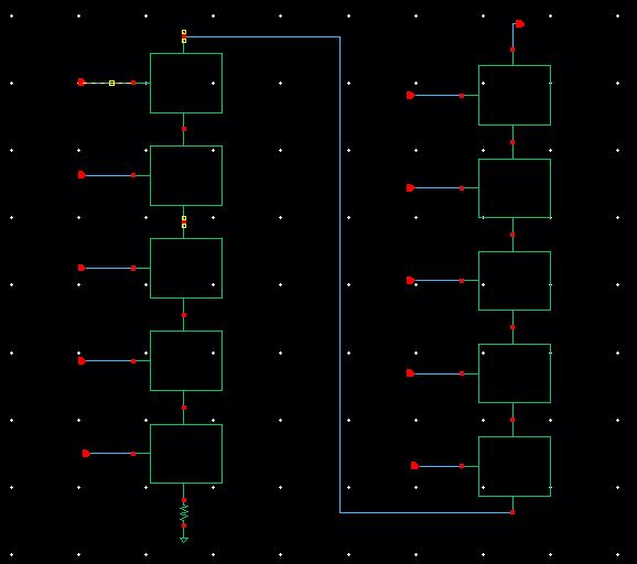
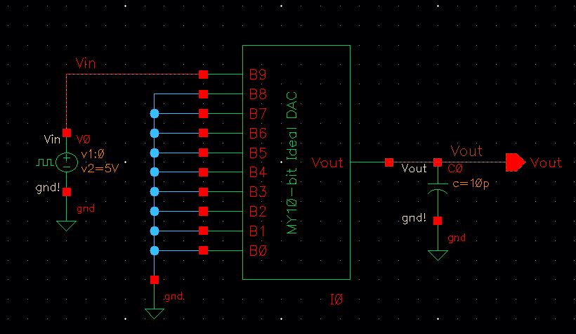
Make a copy of Ideal_10-bit_DAC and label it Mydesign_10-bit_DAC. Open the schematic for Mydesign_10-bit_DAC delete everything. Here we will use the symbol we created earlier (press i for Instance->browse->Find lab2 in Library->click 2R_R) . Place 10 of the symbol in series with one end connected to Ground and the other connected to Vout.
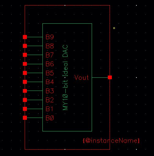
From the library manager go to the sybol for the DAC. Delete VDD, Vrefm and Vrefp.
Deternmine
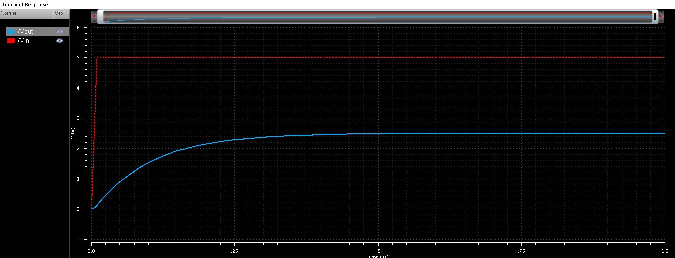
the output resistance of the DAC. First connect a 5 volt puls to B9
port and ground the others, which will give the binary code for 512. To
determine the LSB (Least Significant Bit) use the equation V/(2^N) =
5/(2^10)=4.88m. The purpose of LSB is to show the minimum voltage
change by multiplying LSB with the binary number we will get a 2.5 V.
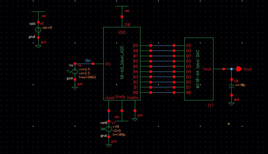
Make a copy of sim_Ideal_ADC_DAC and label it sim2_Ideal_ADC_DAC. Open the schematic and replace the current DAC with the symbol from Mydesign_10-bit_DAC. Since we deleted Vdd, Vrefp, and Vrefm from our DAC symbol we can remove the wires attached.
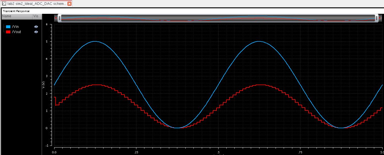
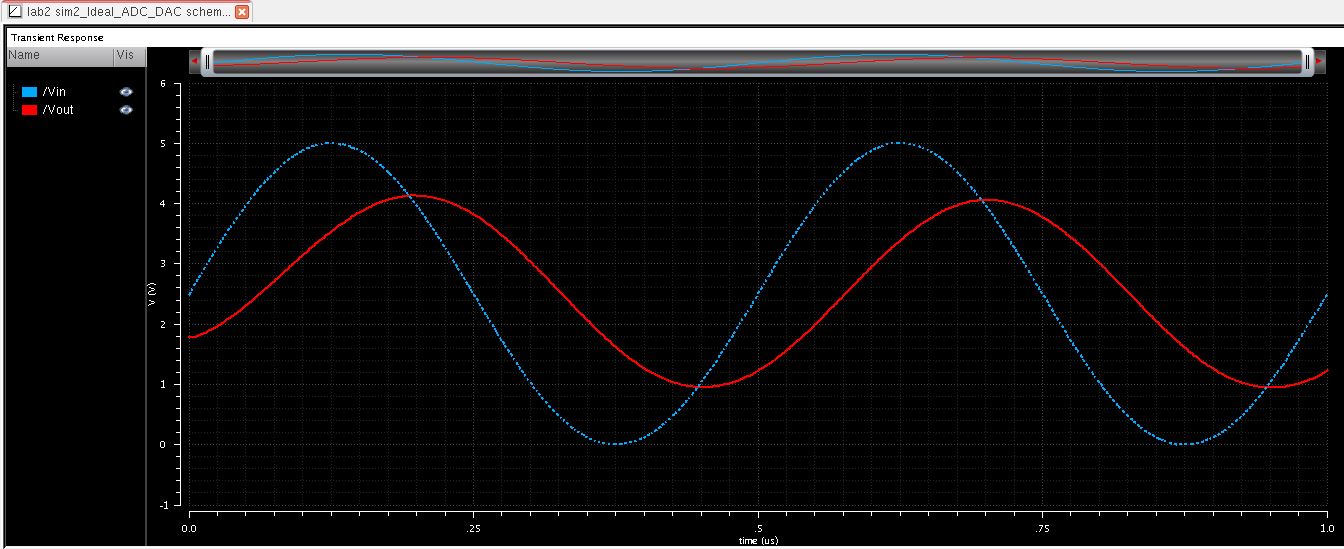
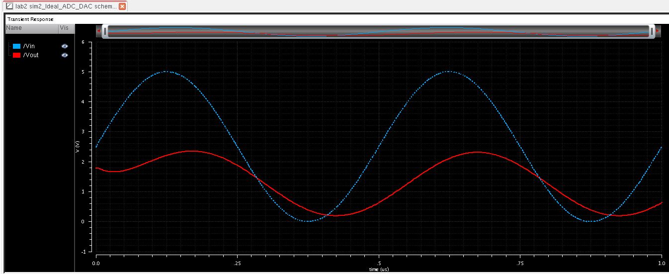
Run simulation as a transient analysis for 1us.
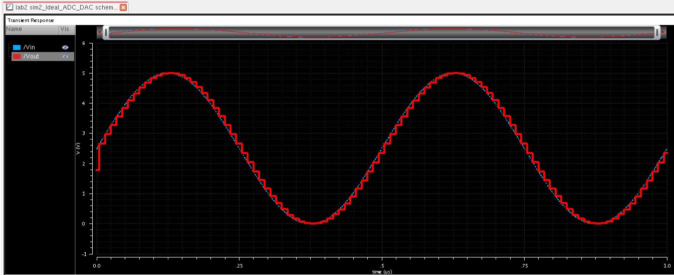
Since the simulation is similar to the prelab we can assume that it is correct. Now we can see what happens when a R, C, and R/C load is placed.
A) 10K Resistor
B) 10pF Capacitor
C) 10K Resistor and 10pF Capacitor
End of Lab 2
Don't forget to back up the file by dragging lab2 from MobaXterm to the desktop and email to yourself.

Return to EE 421L Labs