Lab 04 - ECE 421L
Authored
by Jeevake Attapattu,
attapatt@unlv.nevada.edu
09/29/2014
Simulation of 3 pin & 4 pin NMOS and PMOS
Using MobaXTerm log into csimcluster.ee.unlv.edu. The first action is creating a backup. Type tar -cvf compbackup.tar CMOSedu/. This will create a tar file
with all the project and homework saved. In place of "date" type in the
date creating the backup. Unce the backup has been created type gzip backupdate.tar. This will create a .tar.gz file witch is significantly smaller.
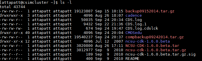
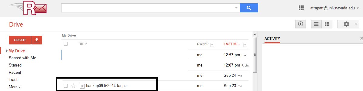
Use MobaXTerm to download the file to your own pc then upload to a backup site such as dropbox or google drive.
Launch Virtuoso.
You will be using previous work from tutorial 1 and continuing the steps in tutorial 2.
Download all tutorials from here.
In the library manager copy the files in lab 3 to lab 4.
We
will be creating layouts for NMOS and PMOS with 3 and 4 pins. Lets
begin with the 3 pin NMOS. Create a new cell view with schematic called
NMOS3.
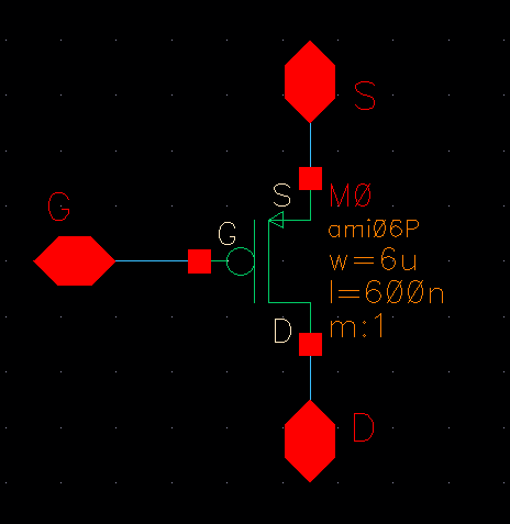
Intanciate and use the part browser. Go to the NCSU_Analog_Parts library and select nmos. Nmos4 is the 4 pin version. Change the width to 6um from the default 1.5um.
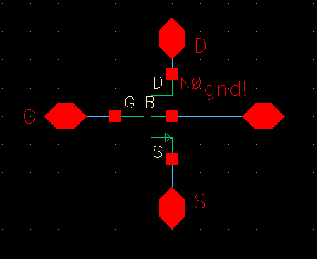
Add G, D, and S inputoutput pins and connect with wires. You should have the schematic below.
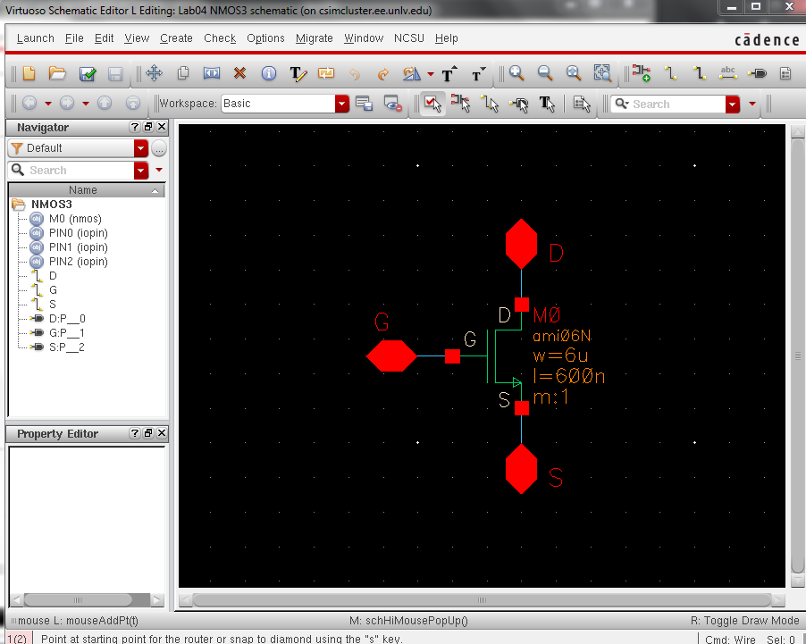
We will not be creating a new symbol as in tutorial 2.
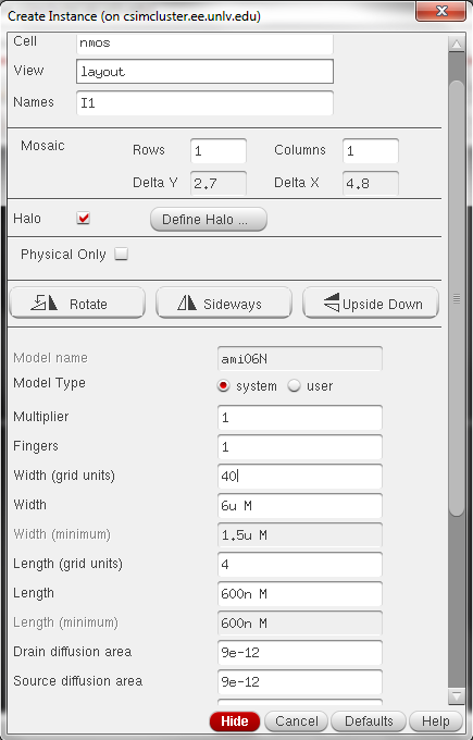
Now lets create the layout. In the library manager select the NMOS3 cellview and create a layout. Use the NCSU_TechLib_ami06 library and use the nmos layout. Change the width on the create instance window to 6um.
You may only see an outline. To change the display options type e and select pin names and set display level stop to 10.
You should now see the nmos layout.
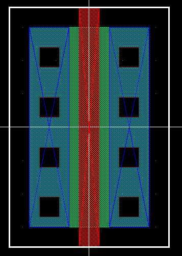
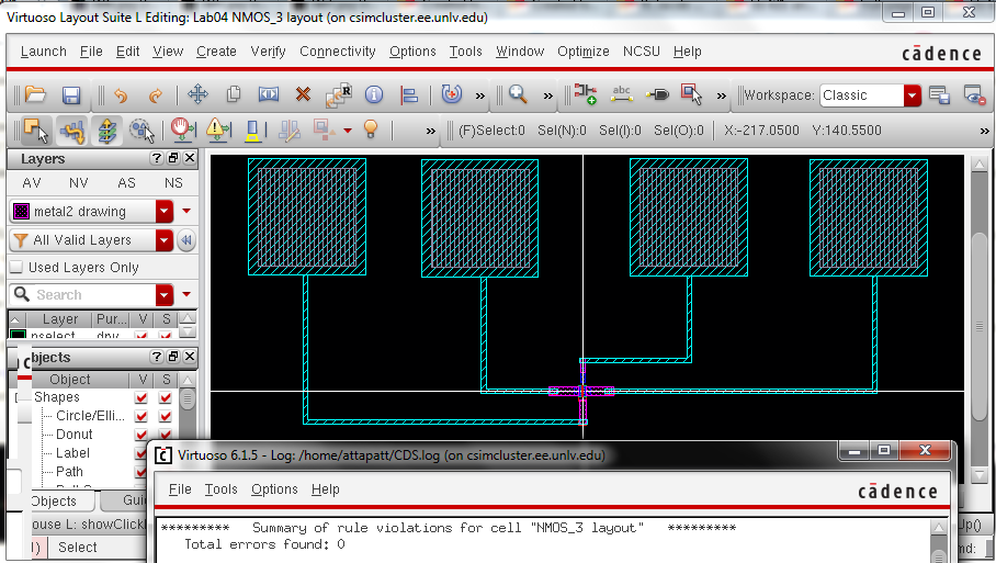
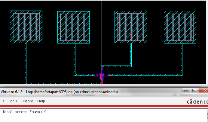
Add m1_poly to create connection from poly 1 to metal 1. Add metal 1 to the over m1_poly and over the taps on the two sides.
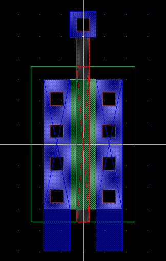
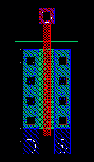
Go to Create->Pin. We will now add the pins to our nmos. Create pins G, D, and S as below.
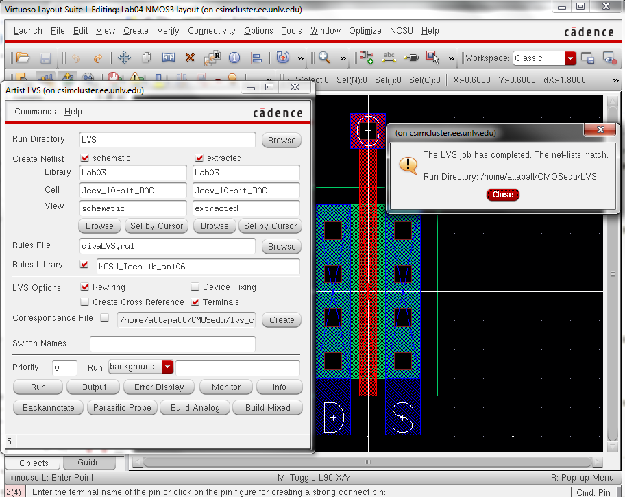
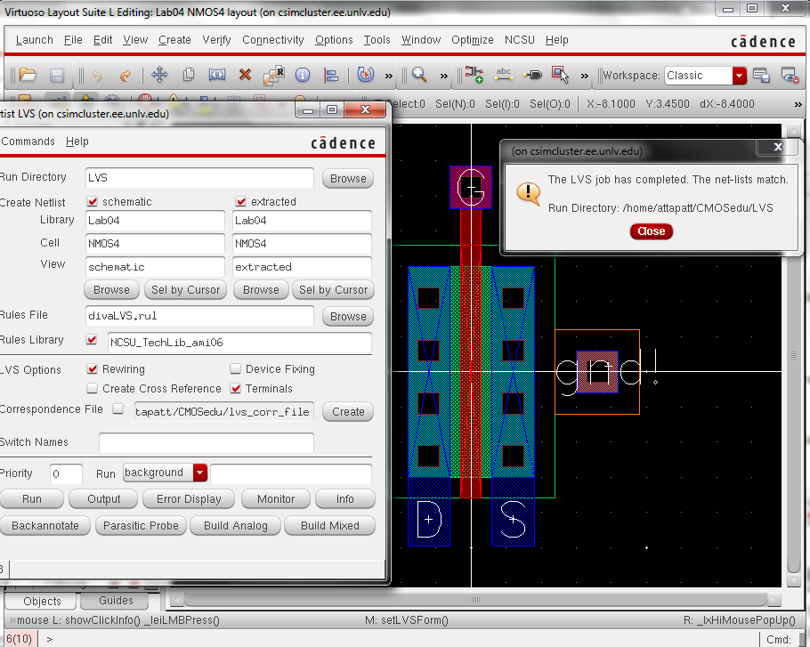
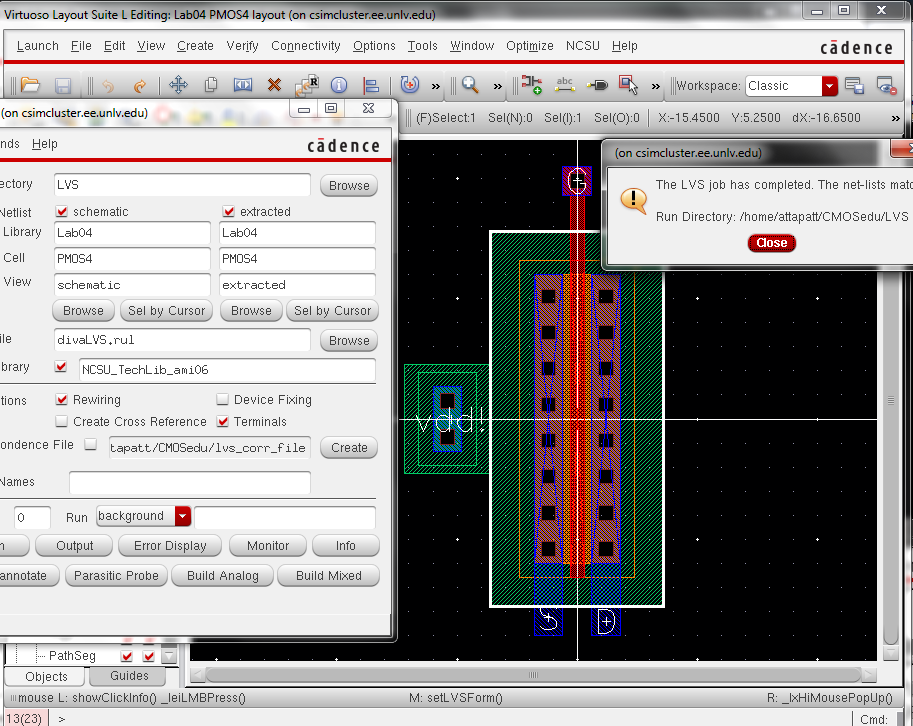
Save and DRC to check for errors. Extract and run LVS. Make sure that the net lists match.
We will now repeat the process for NMOS with 4 pins. Call the new schematic NMOS4. The 4th pin, the bulk must be set to gnd!.
Now the 3 pin PMOS. Call the new cell view PMOS3. Change the width to 6um from 1.5.
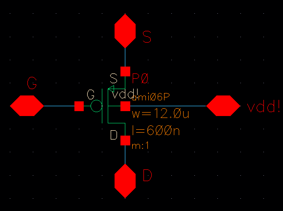
The last to get created is a PMOS with 4 pins. Call the cell view PMOS4. Change the width to 12um from 1.5um.
End Prelab
___________________________________________________________________________
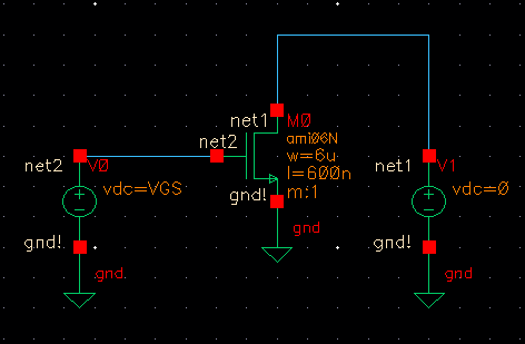
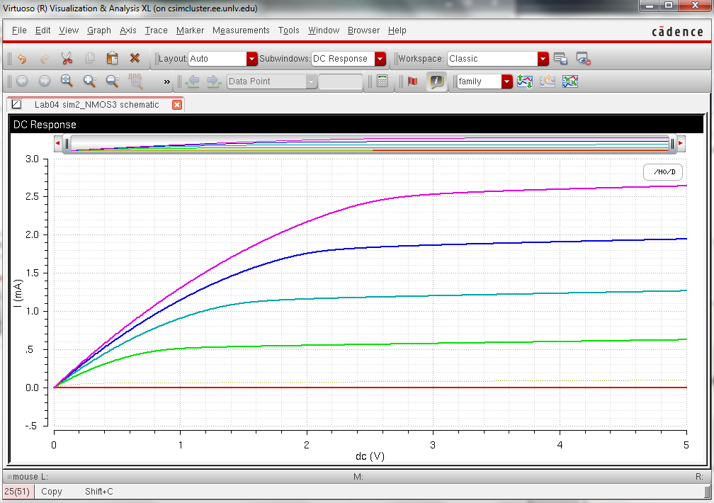
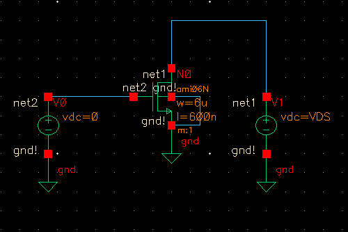
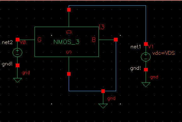
Now we can create some I-V cuvres. Lets begin with the 3 pin NMOS. Create a new schematic called sim2_NMOS3. Add the 3 pin NMOS with W = 6um L = 600nm. Add two vdc voltage
sources. Connect one to the drain and one to the gate. Set the dc
voltage of the gate voltage supply as VGS. Set the drain voltage supply
as 0.
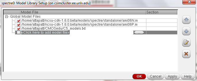
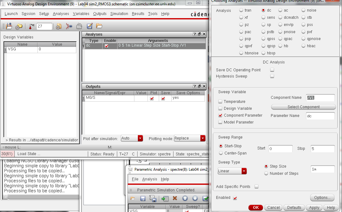
Check and save and launch ADE-L. Go to Setup->Model Libraries. We need to include the models to use. The libraries for the C5 process can be downloaded from here. Go to ncsu-cdk-1.6.0.beta->models->spectre->standalone. Select ami06N.m and ami06P.m.
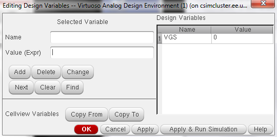
Go to Variables->edit. Add VGS with initial value 0.
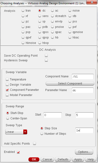
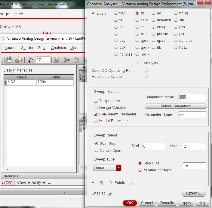
Now
choose the analysis method. Use dc analysis. Select component
parameter. We will sweep V1 with dc values. Set start and stop
values at 0V and 5V respectively. Change sweep type to linear and set
step size to 1m.
The output that we will be plotting is the current through the NMOS.
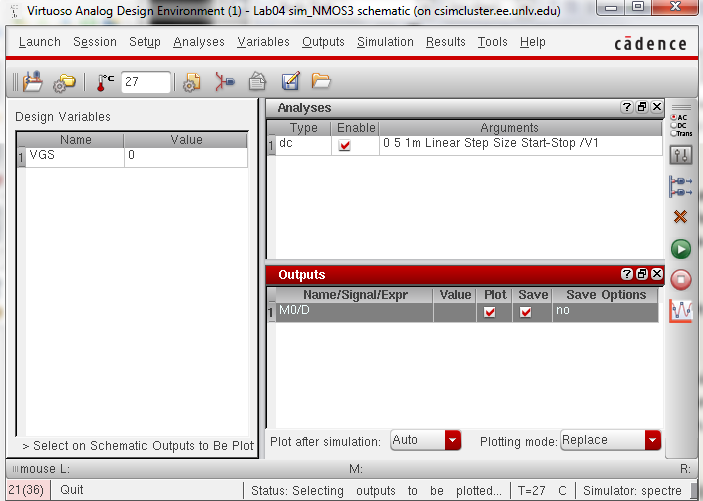
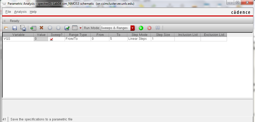
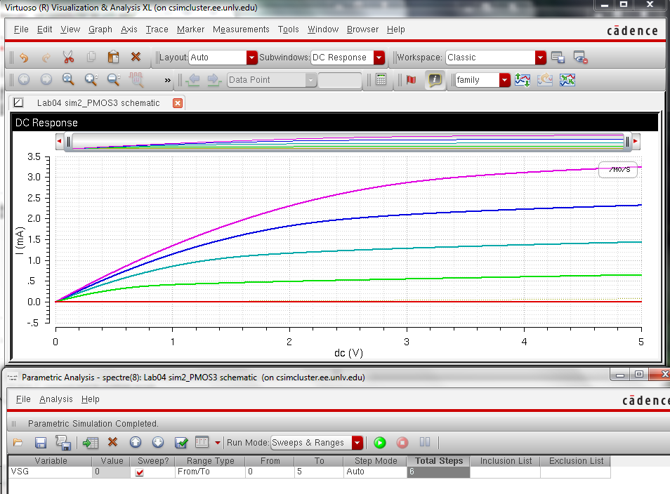
Go to Tools->Parametric Analysis. Set the parameters as below.
Hit green run button. You should see something similar to the graph below.
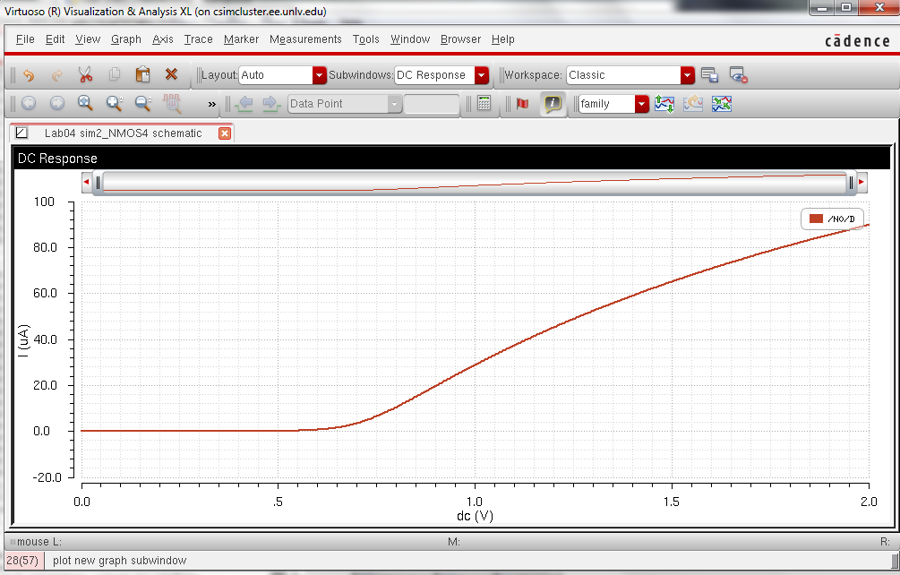
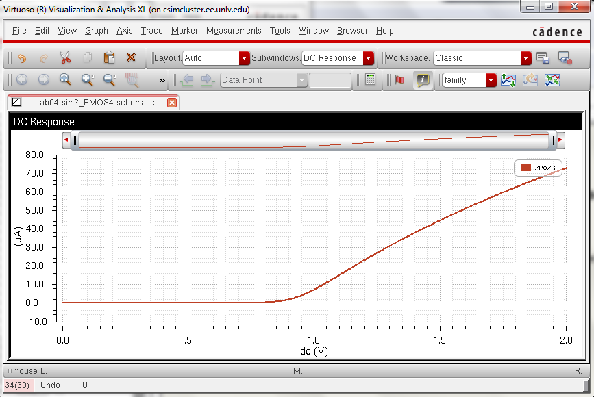
Before exiting save the current state. Copy the files in sim2_NMOS3 to sim2_NMOS4. Open the schematic and replace nmos with nmos4. Connect B to ground. Keep W = 6um and L = 600nm. We will be plotting ID v. VGS with VDS = 100mV. VGS will go from 0 to 2V in 1mV steps. So change the settings on the power supplies as below.
Launch ADE-L and load state. Set the parameters as below.
Since we are plotting for only one value of VDS we do not need to go to parametric analysis. Simply hit run.
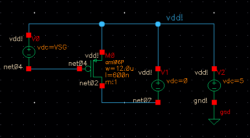
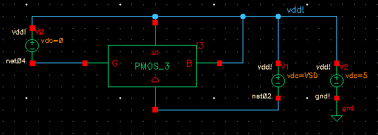
Lets repeat the process for the PMOS. Copy sim2_NMOS3 to sim2_PMOS3. Open the schematic. Change VGS to VSG. Add another voltage source and set it to 5V. Name the wire on top as vdd!. Change the nmos to pmos and set W = 12um and L = 600nm.
Launch ADE-L. Load state. Remeber to change the current name and VGS to VSG. Run parametric analysis as done for the 3pin nmos simulation.
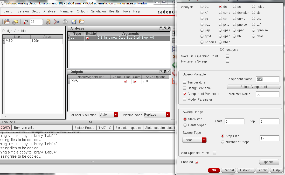
Before exiting save the current state. Copy the files in sim2_PMOS3 to sim2_PMOS4. Open the schematic and replace pmos with pmos4. Connect B to vdd.
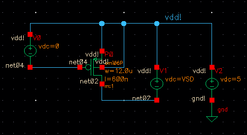
We will be plotting ID v. VSG with VSD = 100 mV
and vary VSG from 0 to 2 V in 1 mV steps. Set the analysis as done in the 4 pin nmos.
Now we need to create probe pads. Create a new cell view schematic called probe pad. We need a no conn. Insatantiate basic->Misc->noConn. Attach a pin to it.
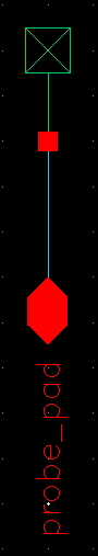
Create
cell view fro cell view for a symbol. After creating the symbol create
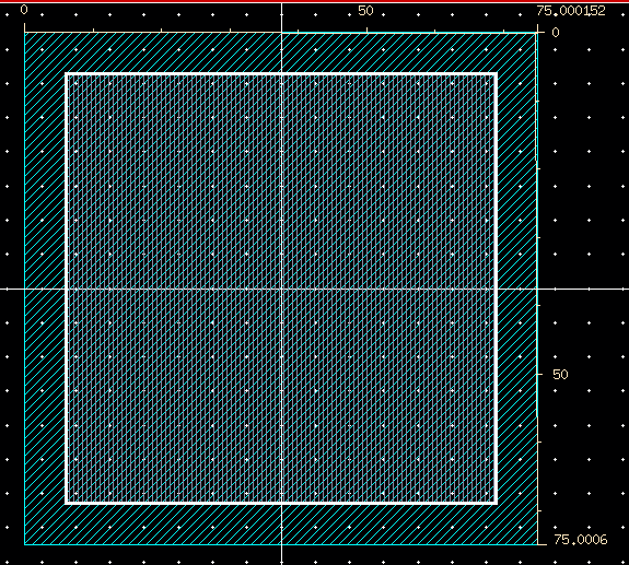
the layout. From previous discussions we know that a 75um square m3 and
63um square over galss works with the design rules. Do not forgetto add a metal 3 pin.
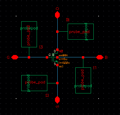
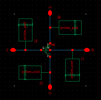
Now
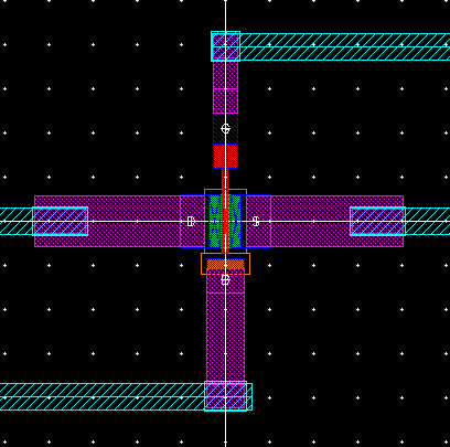
create a schematic for a 4 pin nmos with probes attached to each pin.
Create the corresponding symbol and layout. Connect the pieces on the
nmos to metal 1. Use m2_m1 from the NCSU_TechLib_ami06 library for via1 s. Then use metal 2 to go between metal 3 of the pads and metal 1 of the nmos. Use m3_m1 as via2s.
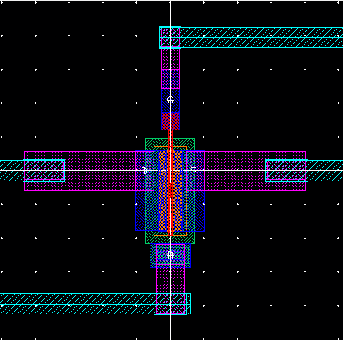
Finally
we do the same thing for the 4 pin pmos. Copy the files you just
created for the 4 nmos call them PMOS_3. Go to the schematic. Click on
the nmos and type q. Change the instance to pmos and W to 12um. Change the top and bottom pins.
Delete
the old symbol and create a new one. Go to the lay out. Change the nmos
for a W=12um pmos. Remove the ptap and insert an ntap. Readjust the
metals as necessary.
Here is a closer look at each.
And the schematics for running the I-V curves of each/
.
Return to EE 421L Labs