Lab 03 - ECE 421L
The first action is creating a backup. Type tar -cvf backupdate.tar CMOSedu/. This will create a tar file with all the project and homework saved. In place of "date" type in the date creating the backup. Unce the backup has been created type gzip backupdate.tar. This will create a .tar.gz file witch is significantly smaller.
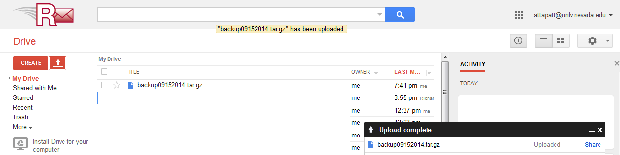
Use MobaXTerm to download the file to your own pc then upload to a backup site such as dropbox or google drive.
Create a new folder in CMOSedu named lab3.
Launch Virtuoso.
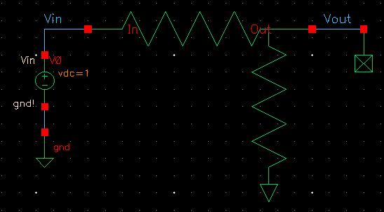
You will be using previous work from lab 1 and tutorial 1. Open the symbol for the divider created in lab 1.
Delete everything except the two pins. Select Create->shape->line. Draw the figure seen below.
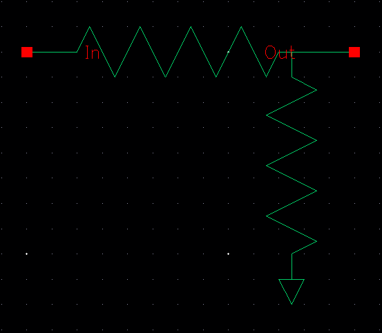
Check and save the new symbol. Go back to the divider simulation. Remove the divider from the schematic and reinsert the with the new symbol. Launch ADE L and load the previous state. Run the simulation You should have the results displayed below.
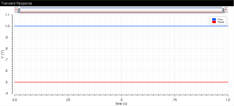
Now we know the new symbol works. We will now create the layout.
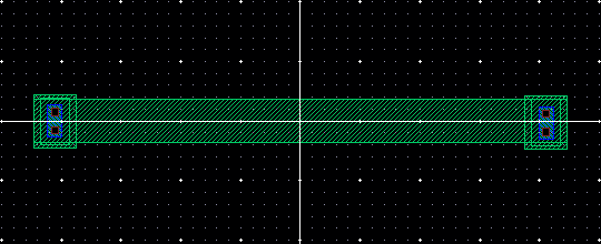
In the Library Manager select the R10k or whichever name you have chosen for a 10k resistor and go to File->new->cell view. Select layout. You should have a window similar to the one below.
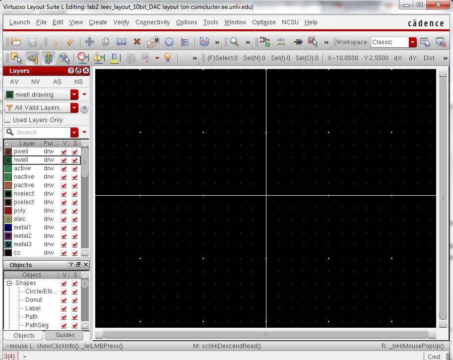
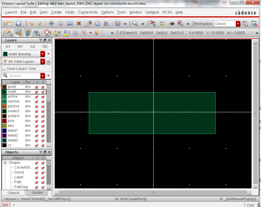
Make sure that you select n-well. We will be using a p-substrate and an n-well process. Now create a rectangle by selecting Create->shape->rectangle OR type R. Create a random rectangle.
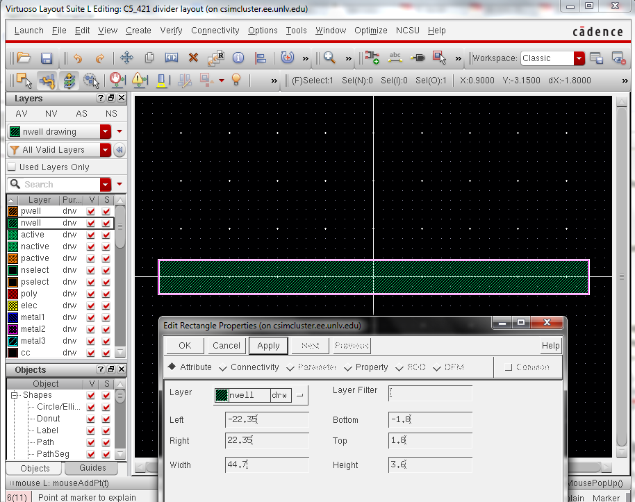
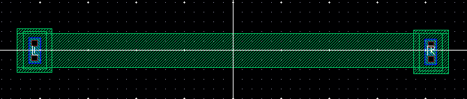
We will be creating 10k resistors. The sheet resistance is 808ohms. Therefor the L/W ratio is approximately 12.4. According to the SCMOS submicron design rules page 16 the minimum width we can use is 12 lambda. This means that L is 148 lambda. In this process lambda is 0.3um. So the layout needs 44.6um for L and 3.6um for W. To use lambda of 0.3um We have to use 44.7um for L.
Select the rectangle and type q. Adjust the width and length. The final image should be similar to the one below. Use DRC to verify.
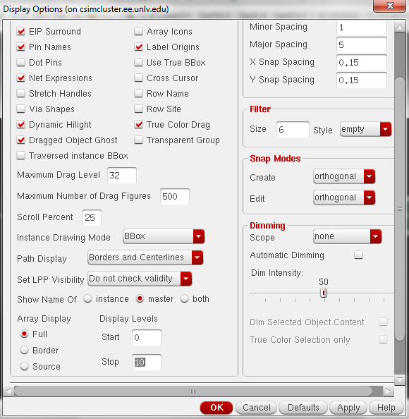
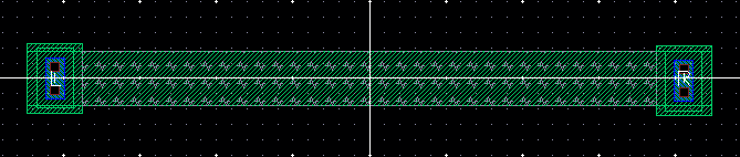
Type e to get the display options. We need to be able to see multiple layers. Change display level stop to 10. And select Pin Names since we will be placing pins.
Now we will be placing taps onto the n-well. Type i and go to the NCSU_TechLib_ami06 and select ntap. Use 2 rows of contacts. Place the ntaps at the ends of the n-well.
Go to Create->pin. Select metal1 and type L for the pin name. Have the display terminal name selected. Place on the left ntap. Repeat process for the right with pin name R.
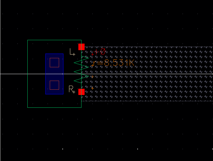
Select res_id to add identification of resistor to the n-well. Draw over the n-well.
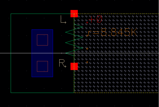
Next do a verify and extract to determine the resistance. Open the extracted file from the library manager and zoom to an end. This will show the final value of the resistor. Here it is 8.531k.
Now we will create a new layout for the divider symbol. Use the library manager to create a new layout in the cell view with the symbol created earlier. Use the resistors created earlier. Select metal1 and add over the pins as below and name them.
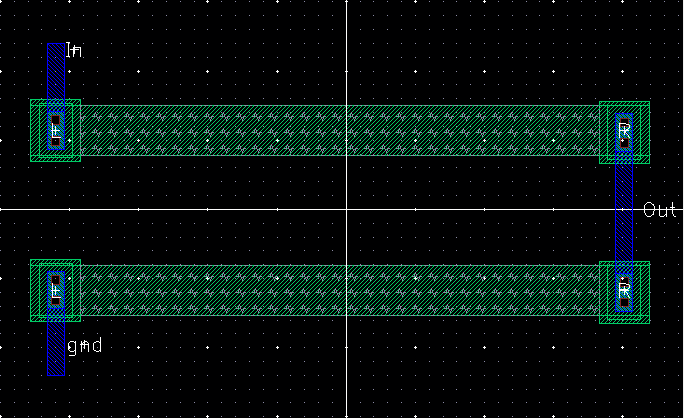
DRC and verify. Then extract. Run LVS. There should be a few errors. You will have to select the pins and edit them. Change gnd to gnd! and In needs to be input not inputoutput out needs to be changed to output.
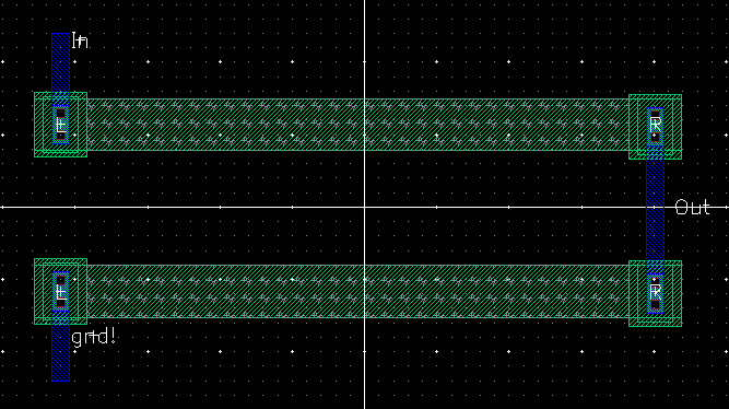
Extract again and run LVS. You should get a net lists match message.
_____________________________________________________________________________________________________
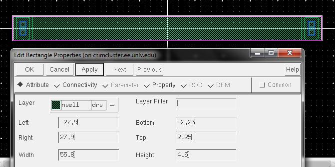
As I chose in the pre lab to get 10k i'll be using 3.6um for W and 44.6um for L. Next place the ntaps. Now place the pins. Make sure that you change the display so that you can see the pins and layers. Since the ntaps are 4.5um high I changed W to 4.5um. To keep the same ratioto get 10k L needs to be 55.7um. To stay on the 0.3um process L needs to be 55.8um.
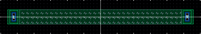
Add the left and right pins. Add the res_id layer and extract. Open the extracted file. Notice the resistance is 8.845k. This is 12% from the 10k we want. However, the exact values of the resistors do not matter in the DAC.
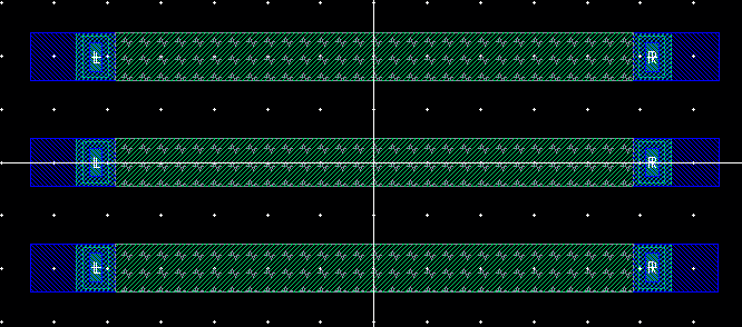
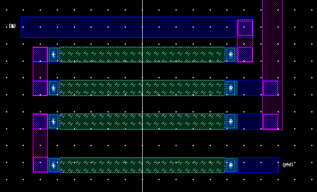
We will need 3 resistors for each bit of the DAC. Make sure that they are 18 lambda away from each other. Add metal 1 rectangles to each side of the resistors.
Add via to the metal 1 connections. I used 3x3 to get more connections.
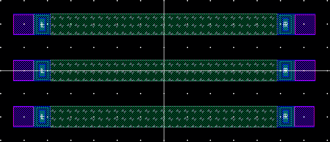
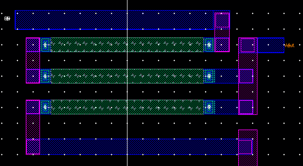
Add metal 2, as below. Then copy to connect the other bits below.
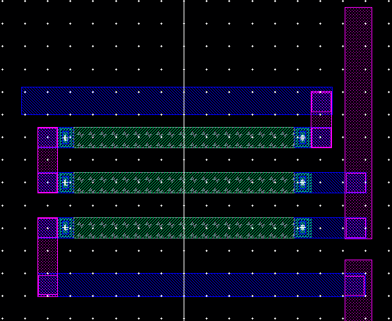
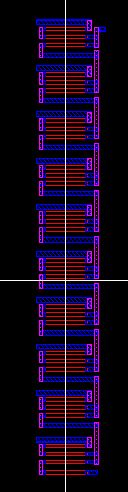
The top and bottom bits will be differenent because of Vout and gnd.
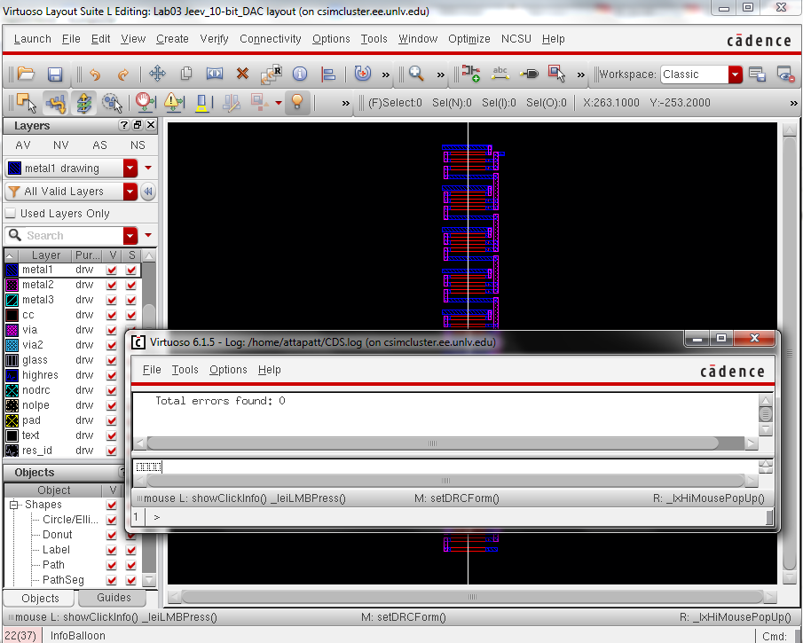
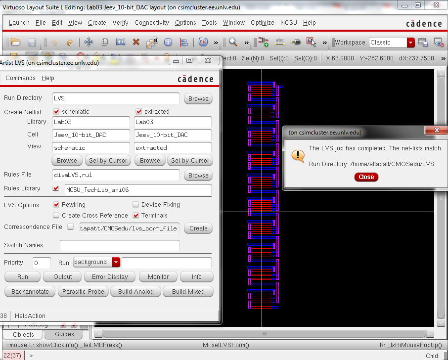
Save, extract, and LVS. There shouldn't be any errors.
The completed lab is located here.
The last step is backing up the files. Below is the backup file uploaded to google drive.