
Lab 7 - ECE 421L


3. Go to the component tab and choose the bus symbol.

4. Now we can left the input/output of the inverter and then right click the other place to make a wire as buses of inputs and outputs. And then put the input/output off-page and connect them to the buses. Don't forget the name the exports as seen below.

Pre-work Tutorial_5:
1. Now let's go through the tutorial_5 learning to use the buses to design the ring oscillator. The follow images show the oscillator with and without using buses.


3. Simulate the ring osillator.

LAB7 Design:
1. First, make the schematic of a 8-bit inverter.

2. Second, two different simulation are shown as below. One is without load. The other is that several outputs has different capacitive loads.


3. Now, designt the 8bit NAND, NOR, AND and OR gates.
NAND GATE

NOR GATE

AND GATE

OR GATE

4. Use LTspice to check the logic function of these four 8-bit gates(NAND, NOR, AND, OR).
NAND GATE


NOR GATE


AND GATE


OR GATE


5. Use these four gates with 8-bit inverters in one schematic and simulate it.

6. Design the schematic of 2-to-1 DEMUX. Then use LTspice to check the demux function. When CLK is high, the A signal (high signal) will be sent to the output. Otherwise the B signal will be sent to the output Z. The simulation proves this circuit working very well.


7. Next, use the bus to design the 8bit demux. Then use LTspice and IRSIM to simulate the circuit. Provide different frequency clock signal and get the different output result. These two inputs are fixed to high or low. When the clock is high, the output will be high. Otherwise, output will be low. Then simulate 8-bit demux by IRSIM. The simulation result shows that Out[0] will follow the VCLK[0]. And the rest of output signals will correctly follow the respective clock signals with a delay.


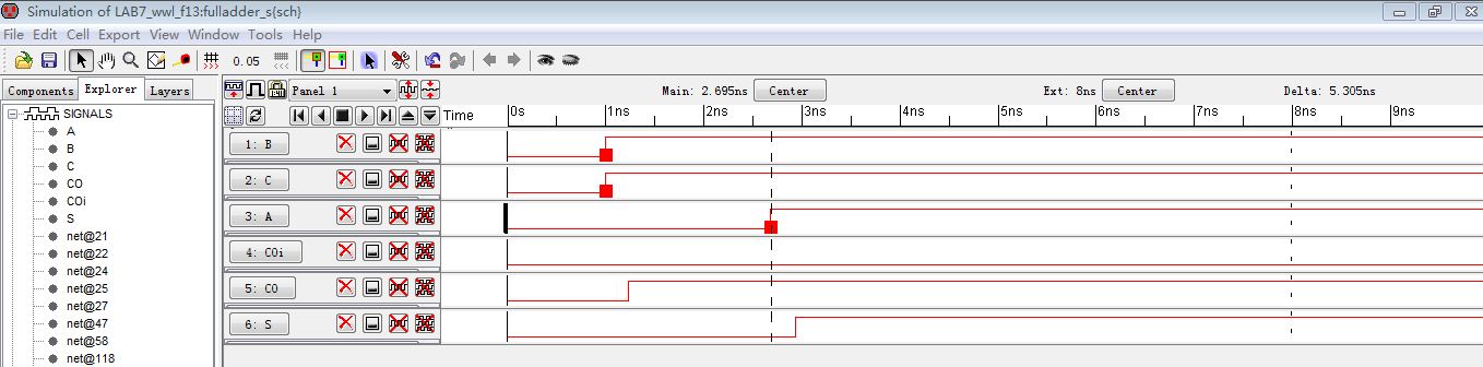
8. Now let's desgin the high-speed full adder as Fig.12.20 in textbook. The schematic is shown in following. The MOSFETs has W=6, L=2. And I also use IRSIM to check its function. When adding B=1,C=1, the CO is 1 and S has no change. When A also becomes 1, the S will become high.


9. Use the buses to design the 8-bit full adder. And also simulate its operation using IRSIM.


10. The next step is to move the layout design. First, let's design the 1-bit fulladder. And pass DRC, ERC, and NCC.


11. Next, it's to design the 8-bit fulladder. And think about how to label the bus so the carry out of one full-adder goes to the carry in of another full-adder. Make sure the final layout passing DRC, ERC, and NCC.


Backup the work directory for future study
