Lab 4 - IV characteristics of NMOS and PMOS devices in ON's C5 process
Authored by Nolan Moore
Date: September 27, 2013
Email: mooren14@unlv.nevada.edu
Lab 4 Working Library
Lab 4 Directions
Prelab:
N/A
Lab Procedure:
In today's lab, we will create PMOS and NMOS transistors in both layout and schematic form in Electric. Having completed the tutorial on creating NMOS and PMOS devices, I will be modifying the devices created in the tutorials for use in this lab.
The MOSFET devices that we will be creating will have the characteristics of 10/2 (3u/0.6u) for the NMOS and 20/2 (6u/0.6u) for the PMOS. We begin by creating the schematics using the regular 3-prong NMOS and PMOS transistors. An off-page node was added to each of the 3 terminals G, D, and S and exported. A ground symbol (NMOS) and a power source symbol (PMOS) are added to the schematics but are not directly connected to anything. These symbols are used to indicate that the bodies of the devices are connected to these sources. The width and height of each of the devices is indicated by the numbers next to the model name.
The icon view for each schematic was created by clicking Make Icon View under the View menu. From there, the default box template was removed and the same transistor symbols used in the schematics were connected to the nodes. The result of creating both the NMOS and PMOS schematics and icons can be seen below
NMOS Schematic and Icon Views
![]()
PMOS Schematic and Icon Views
![]()
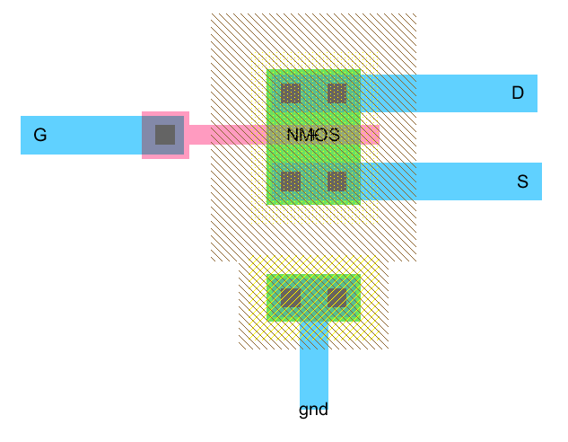
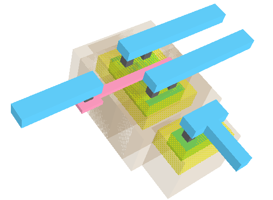
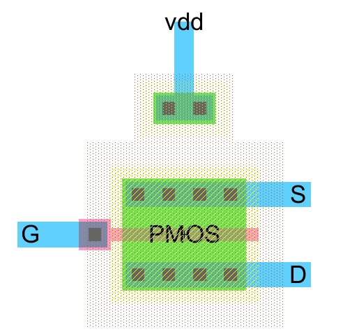
Next the layouts for the devices were to be made. As noted previously, the layouts seen here are based on the layouts created as a result of following Tutorial 2. As we can see in the following images of the layouts created, the width of the PMOS transistor is twice that of the NMOS, reflecting the 20 to 10 widths seen on the schermatics earlier.
As seen in the following images, the bodies of the NMOS and PMOS have been connected to ground (gnd) and power (vdd), respectively. These reflect the extra symbols used in the schematics we saw previously. Unlike in the schematic and icon views, we must export the gnd and vdd nodes used in the layouts. Electric recognizes these as the general ground and power nodes commonly used in the schematics, making it unnecessary to export them in the schematic. Performing an NCC check on the layouts reulted in no errors.
NMOS Layout (2D and 3D)
PMOS Layout (2D and 3D)

Finally, we simulate the schematics/layouts. We create new cells using the icons we created earlier, along with a bit of SPICE code in each cell. The icon nodes are connected to the proper arcs. The simulation results for each of the two devices are shown below their respective circuits.
Simulation of NMOS transistor


Simulation of PMOS transistor
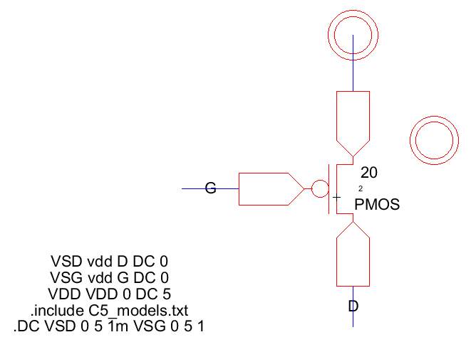

As we can see from the results, the schematics/layouts were properly built as the IV curve is correct.
Return Home