Lab 3 - ECE 421L
Pre-lab
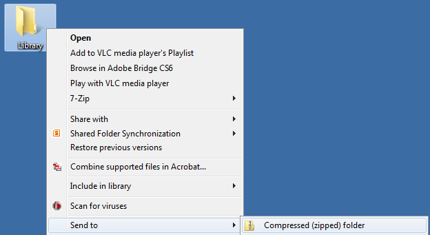
First, to back-up all previous work for the lab and the course, I zipped the folder containing the Electric library and associated files.
To zip the folder, right-click the folder and go to Send to -> Compressed (zipped) folder
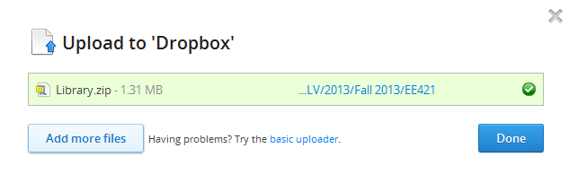
Next, I uploaded the zip file to the back-up service Dropbox.
I then made sure that I finished Tutorial 1 located here.
Lab
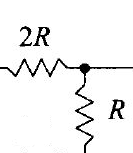
This lab focuses on laying out the 10K resistors previously used to implement the DAC in lab 2.
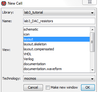
To start, I created a new cell for a layout and named it "lab3_DAC_resistors".
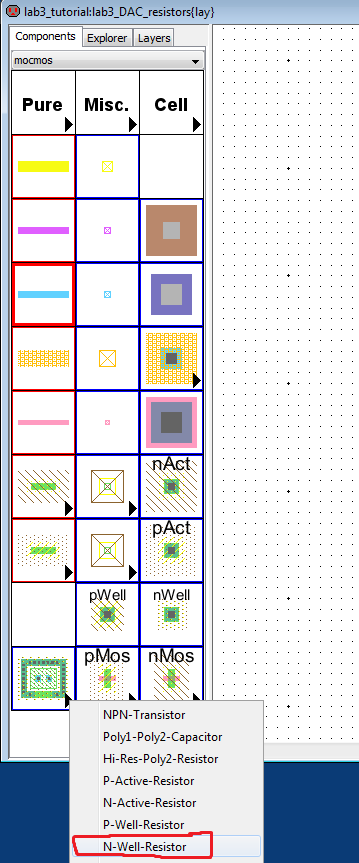
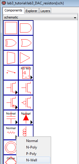
We will be using n-well resistors so, in the components tab, I selected the n-well resistor component and placed in in the layout view.
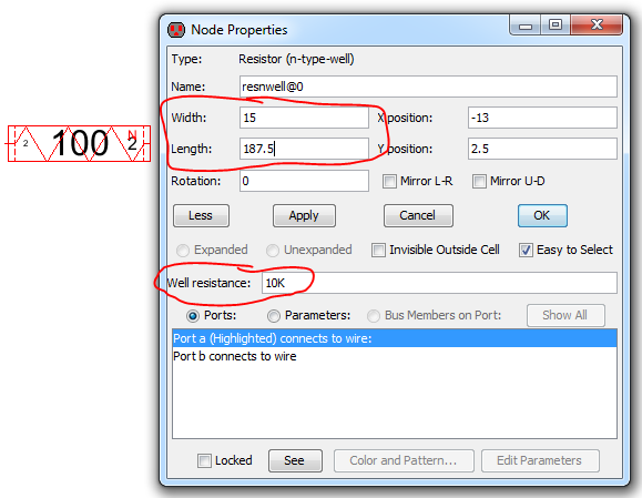
With the resistor placed, I then set the width and length according to the process information from MOSIS.
To find the correct width and length, I went to the information page for the C5 process located here.
Next, I scrolled down and selected the link Test Results for ON Semiconductor C5F/N runs and then chose V35G on the page that follows.
This leads to the page here which contains the information necessary to select the length and width of the n-well resistor.
From that page we can see the sheet resistance for an n-well is 800 ohms/square.
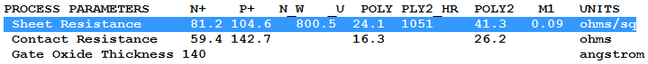
We know the minimum width of n-well is 12 lambda so using a width of 15 and the equation for resistance R=(Sheet Resistance)*(Length/Width) we can plug in values for everything necessary to find the length for a 10K resistor.
10000=(800)*(Length/15)
Length=187.5
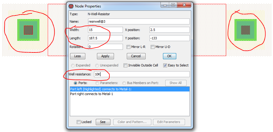
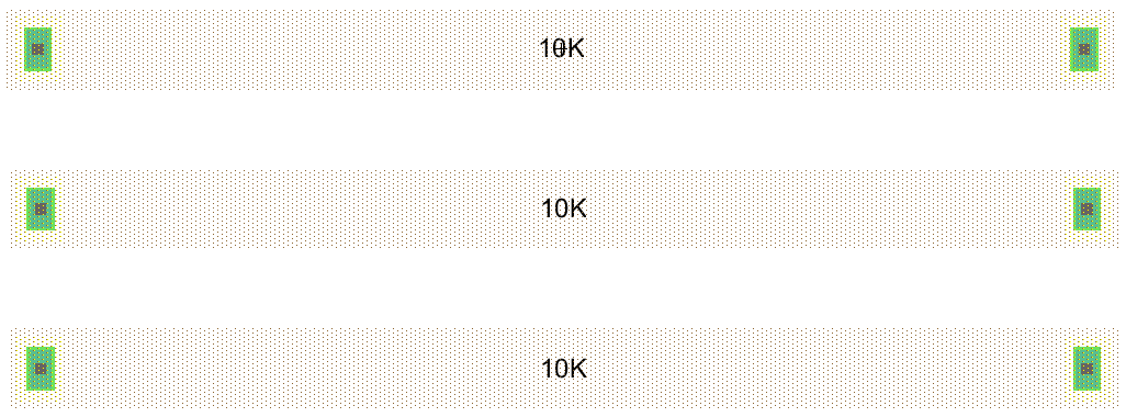
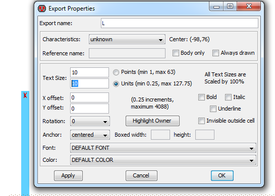
To change the length and width of the n-well resistor click near either of the circled pins and query (ctrl+I by default) to edit the values. Also, set the well resistance to 10K.
You can then select the 10K text and make it bigger by querying it and changing the text size.
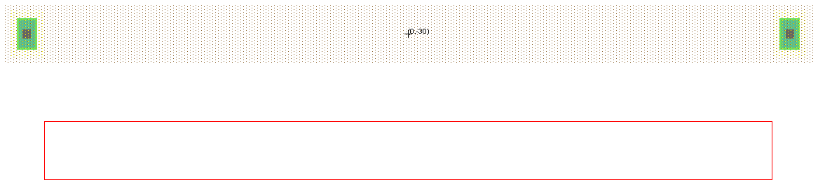
If you use the measurement tool to verify the length and width were applied correctly you can see that Electric measures the length from pin to pin as opposed to the whole resisitor:

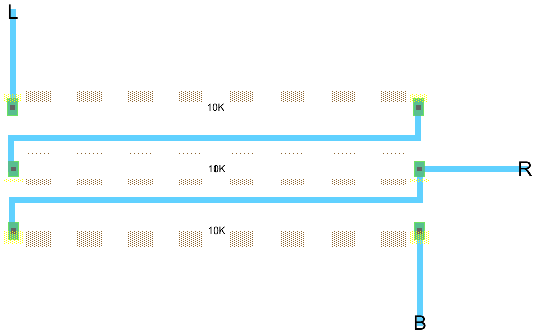
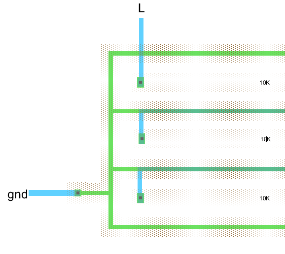
To layout the component we want to make we need 3 n-well resistors, so I selected the n-well resistor and copied it two times below the original. I kept the distance between each resistor at 30 and made sure that there was no change in the x-axis between resistors.
After copying two times and keeping the correct spacing I ended up with:
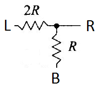
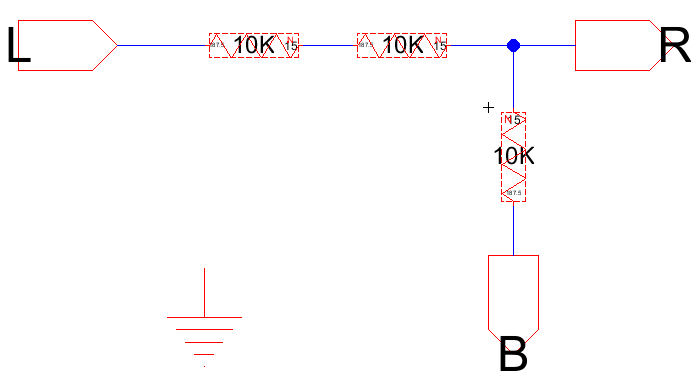
Next, I made the connections between the resistors using metal 1 by selecting each pin and right clicking to add connections. I also added extra connections for exporting the left, right, and bottom of the created component to match the schematic below.
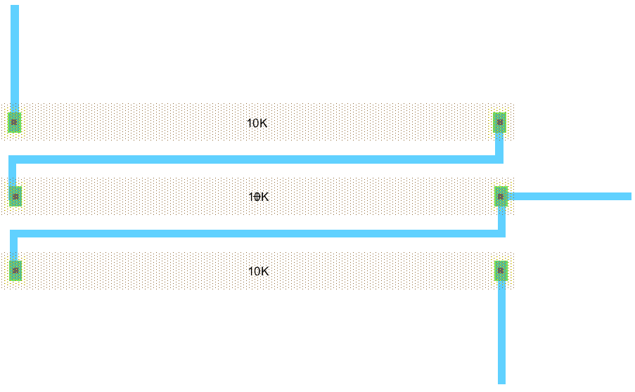
To export the left, right, and bottom, I made sure I was selecting the node by holding ctrl and clicking the end of the wires sticking out, then pressing ctrl+e to create an export.
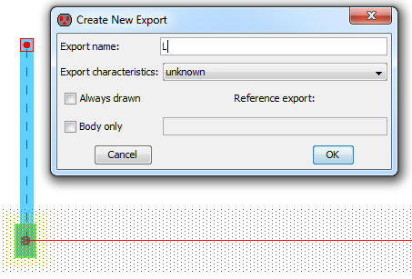
I then ctrl-clicked until I selected the L and changed the text size to 10 to be more visible.
I then repeated these steps to add exports for the right and bottom.
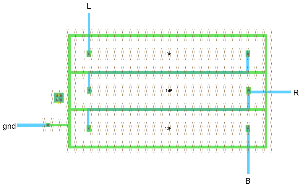
I then selected the pAct component and added a border around the resistors placed so for to better insulate them from outside noise. After placing the node, right click around to add the border.
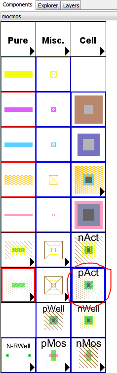
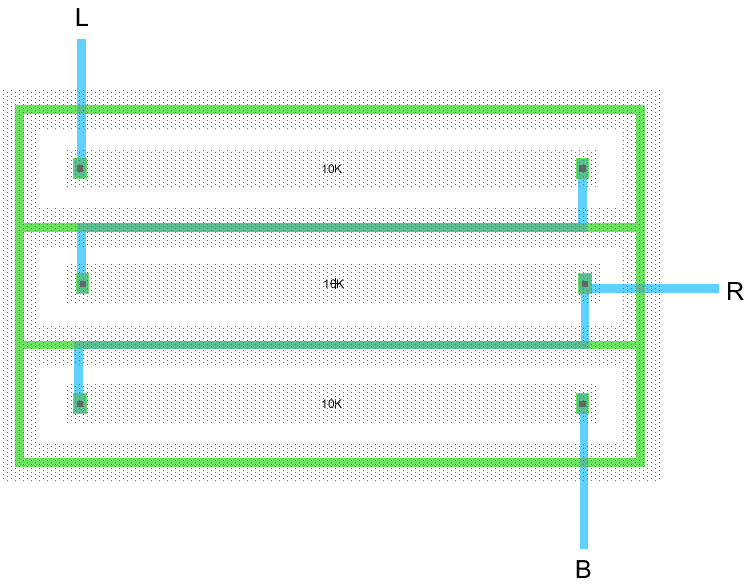
Next, I added another pAct node and created and exported a connection for ground.
To pass the well check I then added an n-well component and changed the size to 12x12 which completes the layout.
Next, to use this component we need to create a schematic and icon view.
So, I created a new cell, selected schematic and named it lab3_DAC_resistors so it is added to the same cell group as the layout.
I added an n-well resistor by clicking the arrow next to the resistor and selecting n-well resistor.
I then selected the placed n-well resistor and changed the length, width and resistance.
Then I copied this resistor two times and connected them together. Next, I placed three off-page components for each left, right and bottom connection and exported each one with the correct label. It's also important to add a ground that's not connected to anything to match the gnd export of the layout and pass the NCC check. The f4 key is useful for removing any extra pins added when connecting the resistors.
Next, I created an icon by going to View -> Make Icon View
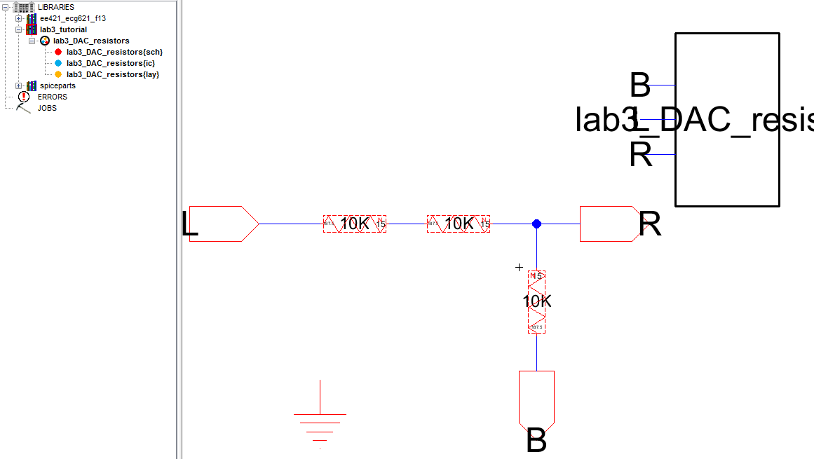
I then modified the icon to make it look more like the final component.
Next, I ran a DRC check (f5 key or Tools -> DRC -> Check Hierarchally) on the design.
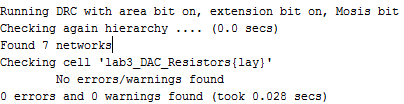
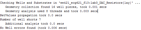
Then an ERC check (w key or Tools -> ERC -> Check Wells)
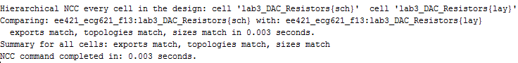
Finally an NCC check (L key or Tools -> NCC -> Schematic and Layout Views of Cell in Current Window).
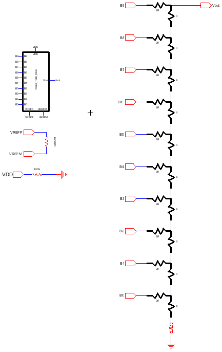
Next, to verify that the component was working correctly I copied the R2R_10bit_DAC schematic from lab2 and named the new schematic lab3_DAC.
I then replaced all of the resistors in the schematic with my newly created component by dragging the lab3_DAC_resistors icon into the lab3_DAC schematic and making all required connections.
I then added an extra 10K n-well resistor on the final bottom component to match lab2's R2R DAC. I also changed the icon view name to Nwell_10bit_DAC similar to how was done in lab2.
Finally, I duplicated the original ADC-DAC schematic from lab2 and named the new schematic lab3_ADC_DAC_sim. I then removed the DAC component (but left all other wires), placed my lab3_DAC component by dragging the icon into the schematic where the old DAC was, selected the lab3_DAC and went to Tools -> Routing -> Auto-Stitch Highlighted Now to make all of the required connections.
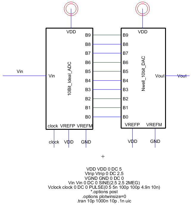
I then ran an ltspice simulation (s key or Tools -> Simulation (Spice) -> Write Spice Deck...)
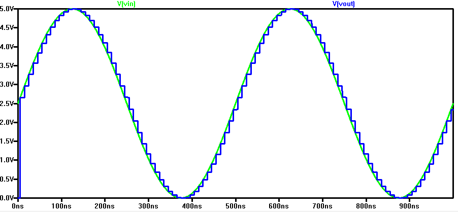
Success! We can see that the layed out component works correctly and provides the same results as lab2.
My jelib file containing lab3_DAC_resistors, lab3_DAC, and lab3_ADC_DAC_sim can be found here.
Backing up everything
I then backed up everything as was done in the pre-lab.