Lab 2 - ECE 421L
Authored
by Ruben Medina,
Email: medina72@unlv.nevada.edu
Date: 9/6/13
Design of a 10-bit Digital-to-Analog Converter (DAC)
Prelab
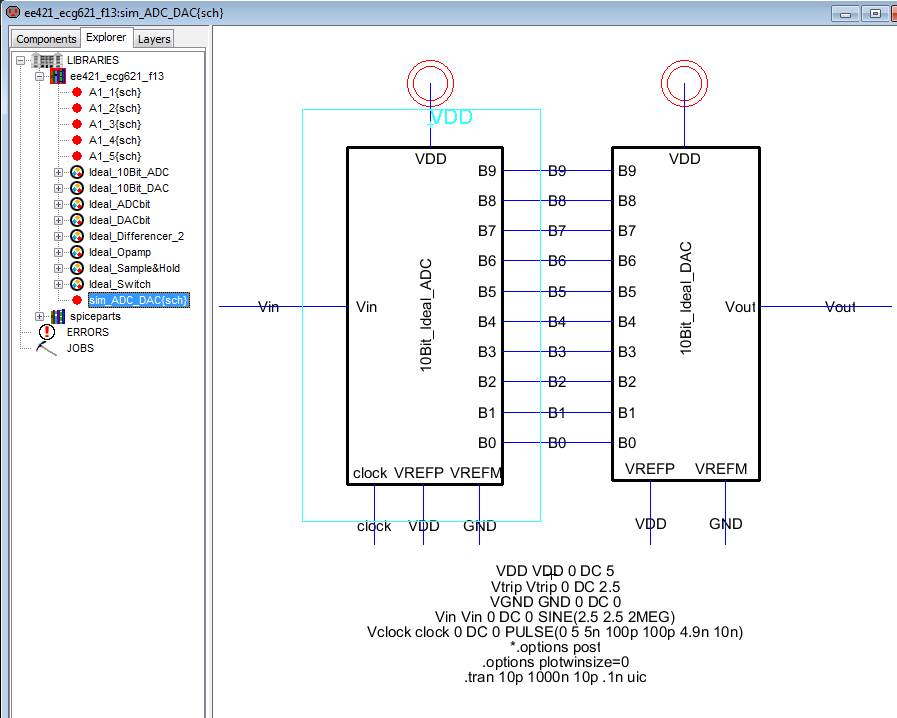
For the prelab, I started by downloading lab2.jelib which contains a simulation example using an ideal 10-bit Analog-to-Digital Converter (ADC) and 10-bit DAC.
I then opened my previously saved ee421_edg621.jelib library and lab2.jelib in Electric.
Next,
to copy the ADC and DAC designs to my library I went to Cell ->
Cross-Library Copy... and then selected the sim_ADC_DAC{sch} cell from
the lab2 panel. Then, by checking the Copy subcells and Copy all related views options I clicked the copy button with arrows pointing towards my own ee421_ecg621_f13 library.
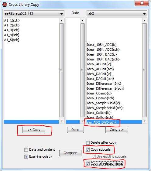
In the explorer pane of Electric I then closed the lab2 library by right clicking on it and choosing Close library. I then saved (ctrl+s) my ee421 library and opened the sim_ADC_DAC{sch} cell.
Lab
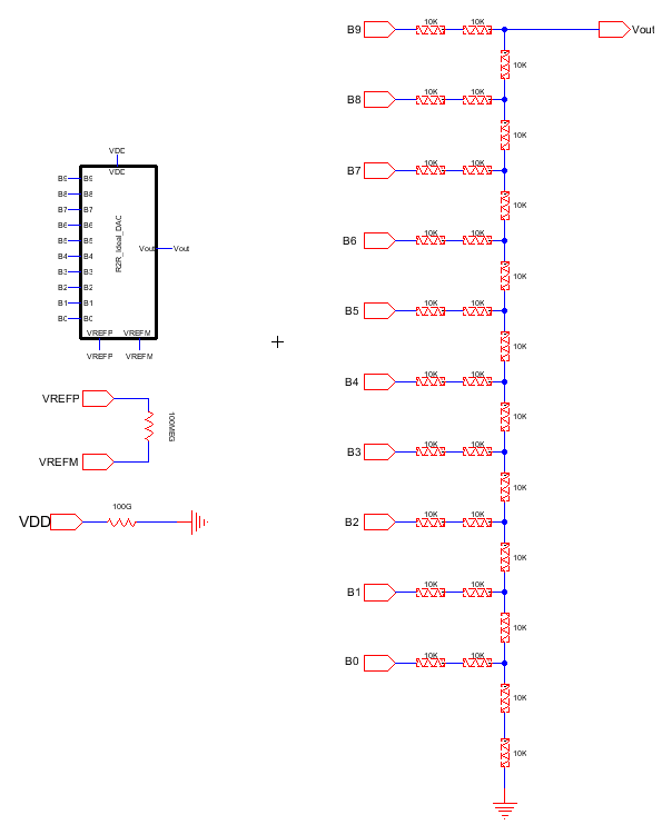
In this lab we'll use n-well resistors to implement a 10-bit DAC.
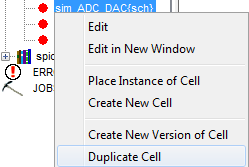
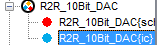
To begin with I duplicated the original Ideal_10bit_DAC that I preivously copied to my library in the pre-lab and named it R2R_10bit_DAC.

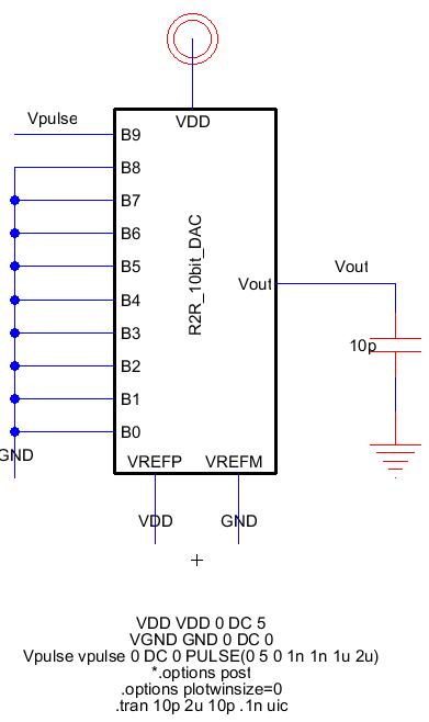
The design we will be replacing the original DAC with is the following:

After
duplicating the original DAC, I deleted the original components
attached to each input (Bx) pin and then recreated the new design using
the n-well resistor component:
After this I checked the new design using Tools -> DRC -> Check Hierarchically (also possible using f5 by default).
We can see that the output voltage is R when you combine the resistors in parallel and series.
Looking
at the above, with R=10K, if you start from the bottom, the 20K series
combination is in parallel with the 20K series combination of B0. This
results in a 10K resistance at the new bottom without the B0 input.
By
repeating this process until B9 you eventually end up with a final 20K
resistance in parallel with another 20K resistance resulting in a final
10K (R) output resistance.
I then checked the delay of this new R2R DAC when driving a 10pF capacitive load.
To do this, I first duplicated the original sim_ADC_DAC schematic:
In this new duplicate cell which I named sim_PULSE_DAC
I deleted the icons already there and dragged the R2R_10bit_DAC icon
(which was created when the original 10bit_DAC was duplicated) into the
new sim_PULSE_DAC cell.
I then grounded pins b0-b8, modified the spice command to add a pulse input voltage to b9, and added a capactior to the output.
For
an RC circuit like what we now have, the time delay of the output is
0.7RC. For the R of 10K used and the 10pF capacitor used the delay of
the output should be 70ns.
Running a simulation for the above results in the following:
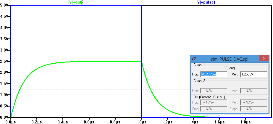
From the simulation results we can see a delay of approximately 70ns which matches the hand calculated expected value.
If
an icon needs to be made for a hand designed circuit in the future,
from the schematic of the circuit go to View -> Make Icon View which
adds an icon for the circuit to the schematic.
After selecting the icon and pressing ctrl+D you can change the way the icon looks.
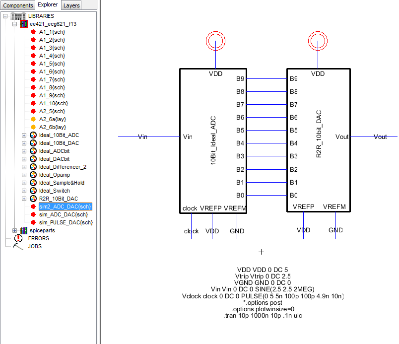
Now, to make sure the newly designed R2R_10bit_DAC works, I duplicated the sim_ADC_DAC cell and named the new cell sim2_ADC_DAC.
I then replaced the original 10bit_Ideal_DAC with the R2R_10bit_DAC icon which can be seen below:
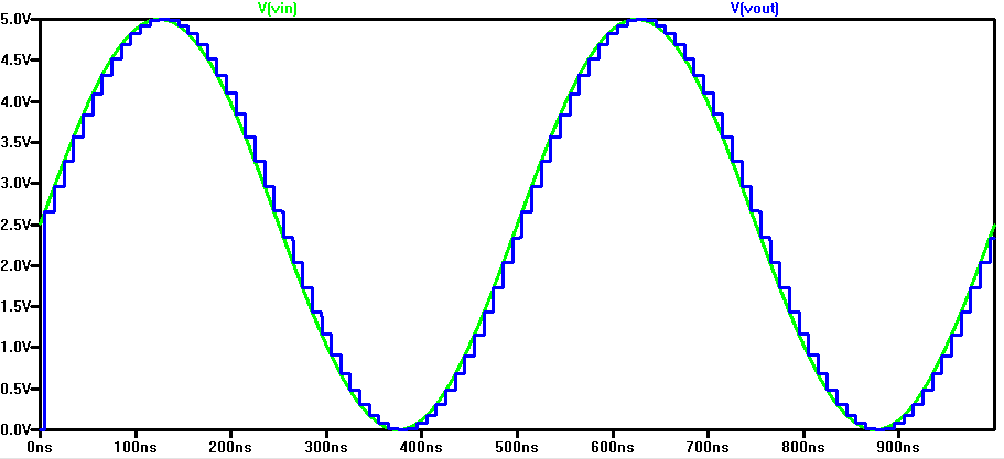
I then verified with simulation that the R2R DAC worked correctly:
Next, I checked what happens when the DAC drives a resistive 10K load:
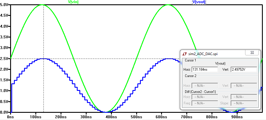
The resistor acts as a resistive divider so with 10K the output is half the input amplitude voltage.
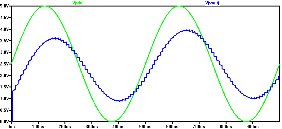
Next, I checked what happens when the DAC drives a capacitive load:
The capacitor creates an RC circuit with the DAC which results in a change in amplitude and delay in output.
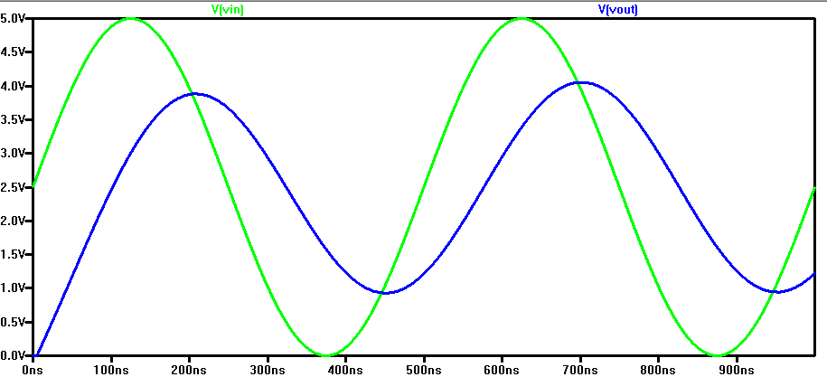
Finally, I checked what happens with a resistive and capacitive load:
The RC circuit in parallel with the DAC creates a change in output amplitude and phase.
As seen above, when the resistive load is 10K there is a voltage divider of half the input voltage.
Finally,
when the switches seen in the original R2R design shown above are
implemented with MOSFET transistors they add an additional resistive
component to the DAC which results in a change in output voltage
amplitude.
Return to my list of labs