EE 420L Engineering Electronics II - Lab 1
2/3/16
For this first lab simulate, and verify the simulation results
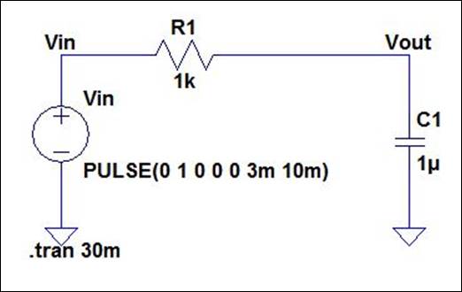
with experimental measurements, the circuits seen in Figs. 1.21, 1.22, and 1.24
(use a 1 uF cap in place of the 1 pF cap) of the book. Your results
should be similar to, but more complete than, the simulation results seen on
pages 17 - 23. In your report, and for each circuit, show the
Experiment
1: Circuit Fig 1.21
Circuit Fig. 1.21
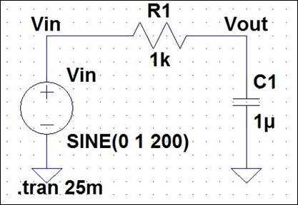
The quantities to
be measured in this experiment will be the transfer function, phase response
and time delay. Theoretical values obtained via hand calculations are shown in
the image below.
Theoretical Values
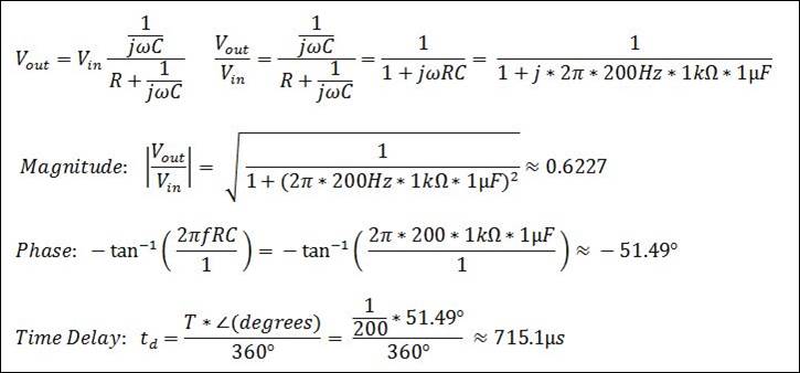
The waveform below
from the LT Spice simulation displays a transfer function magnitude of
approximately 622.5mV and a time delay of approximately 717µs.
Simulation Values
Fig 1.21 Transient Analysis
An AC analysis was
performed to obtain the phase response. The circuit and resulting waveform are
shown below. The simulation resulted in a phase response of approximately -51.4![]() . Included below
these images is another method of obtaining similar information as obtained in
the transient analysis and the AC analysis. This is
done to demonstrate the versatility of LT Spice as an analytical tool.
. Included below
these images is another method of obtaining similar information as obtained in
the transient analysis and the AC analysis. This is
done to demonstrate the versatility of LT Spice as an analytical tool.
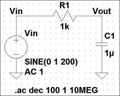
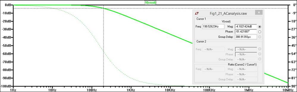
Fig 1.21 AC Analysis Method 1
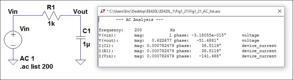
Fig 1.21 AC Analysis Method 2
Comparing the
theoretical values to the simulated values above reveals close approximations
between the two different methods of analysis.
Experimental
values are shown below in the oscilloscope images captured during the
experiment. The phase response will be calculated using the time delay equation
found in the theoretical values and solving for degrees.
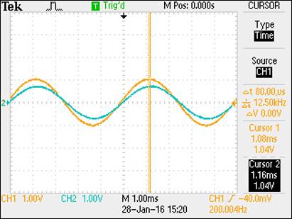
The figure on the
left displays an amplitude of 600mV. The
figure on the right displays a time delay, ![]() of 800µs. The calculated phase response was
-57.6
of 800µs. The calculated phase response was
-57.6![]() . These values
fall within the range of the simulated and theoretical values.
. These values
fall within the range of the simulated and theoretical values.
Experimental Values
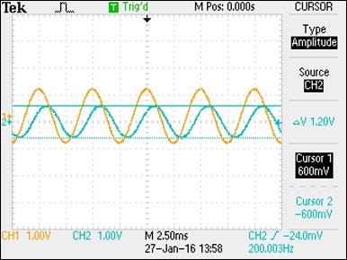
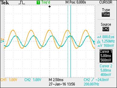
Fig. 1.21 Amplitude
Fig. 1.21 Time Delay
The table below shows a comparison of the experimental,
theoretical and simulation values.
|
Fig 1.21 |
| |
|
|
|
|
|
|
|
|
Simulation |
0.6224 |
-51.49 |
717.3µ |
|
Theoretical |
0.6227 |
-51.49 |
715.1µ |
|
Experimental
|
0.6000 |
-57.60 |
800.0µ |
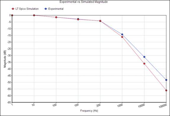
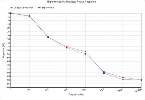
The circuit in Fig. 1.21 was used to generate a table showing
representative values for the magnitude and phase response. These values were
obtained via experimentation and simulation with the results given in the table
and plots below. The frequency at 159Hz represents the cut-off frequency. The plot verifies the decrease in magnitude
that occurs once the frequency exceeds the cut-off frequency. This data
indicates the circuit acts as a low pass filter, accepting only frequencies
below 159Hz and rejecting frequencies above 159Hz.
|
Frequency
(Hz) |
Experimental
Magnitude(dB) |
Experimental
Phase ( |
SImulation Magnitude (dB) |
Simulation
Phase ( |
|
|
|
|
|
|
|
1 |
0.00 |
0.00 |
0.00 |
0.00 |
|
10 |
0.00 |
-4.20 |
0.00 |
-3.61 |
|
100 |
-1.41 |
-32.4 |
-1.44 |
-32.1 |
|
159 |
-2.85 |
-46.37 |
-3.04 |
-45.1 |
|
200 |
-4.21 |
-54.7 |
-4.13 |
-51.6 |
|
1k |
-14.3 |
-79.2 |
-16.1 |
-80.9 |
|
10k |
-31.1 |
-86.4 |
-36.0 |
-89.1 |
|
100k |
-48.3 |
-89.9 |
-56.0 |
|
Experiment
2: Circuit Fig 1.22
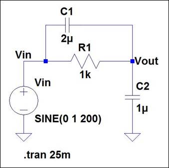
The circuit in Figure 1.22 is similar to the RC circuit in Fig.
1.21 with the addition of a 2µF capacitor in parallel with the 1kΩ
resistor. Theoretically, the capacitor in parallel with the resistor should
reduce the amount of loss in the strength of the signal when compared to the
circuit in experiment one. The same process will be used as in experiment one
to compare values and analyze results.
The comparison of values will be included in a table following the
images containing the relevant quantities measured during each different type
of analysis.
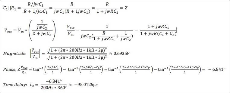
Circuit Fig. 1.22
Theoretical Values
Simulation Values
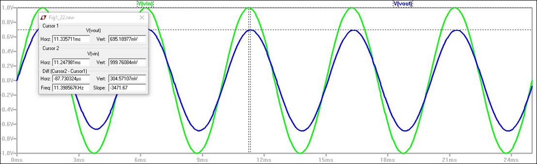
Fig. 1.22 Transient
Analysis
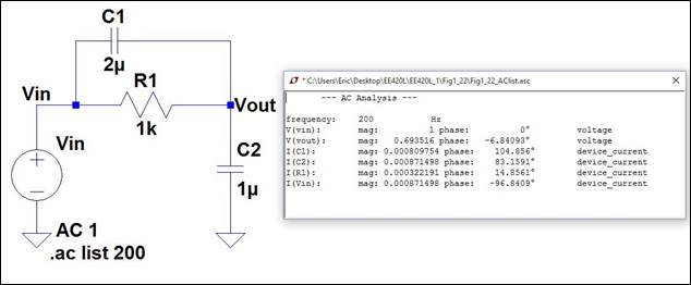
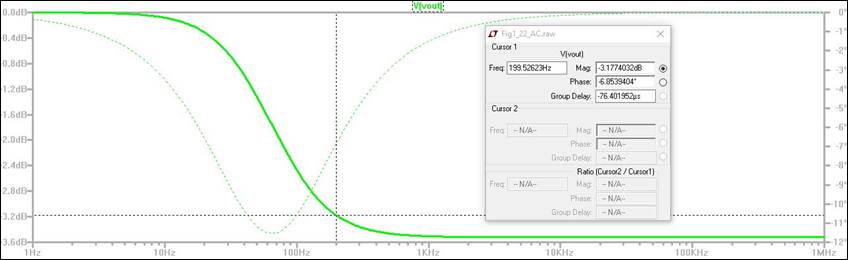
Fig. 1.22 AC Analysis
Experimental Values
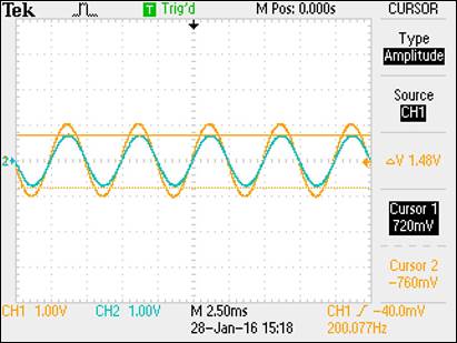
Note the similarities between the waveform outputs in the
simulation versus the oscilloscope. The values are in the range expected when
compared to hand calculations. The table below displays a comparison of
measured values. Variances are likely due to occur between the different
methods of analysis due to differences in the techniques themselves. For
example, the oscilloscope values may differ from the simulation values due to
the difficulty in aligning the cursors on the oscilloscope precisely enough to
gather accurate data.
|
Fig 1.21 |
| |
|
|
|
Simulation |
0.6952 |
-6.854 |
76.40µ |
|
Theoretical |
0.6935 |
-6.841 |
95.01µ |
|
Experimental
|
0.7200 |
-5.760 |
80.00µ |
As seen in the table above, the capacitor in parallel with the
resistor served to lower the impedance and reduce the loss in signal strength
compared to the circuit in experiment one. The experimental magnitude
of the transfer function in circuit one was approximately 600mV versus
approximately 720mV for the circuit in experiment two. There was also a
noticeable reduction in the time delay and the phase response for experiment
two.
Experiment
3: Circuit Fig 1.24
The circuit in Fig. 1.24 is the same as the circuit in experiment one,
but for experiment three the input has been changed to a pulse. Using the pulse
will allow calculation of the delay time and the rise time of the signal. The
results of the analysis are displayed in the images below. The measured values
will be displayed in a table below.
Circuit Fig 1.24
Theoretical Values
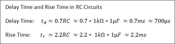
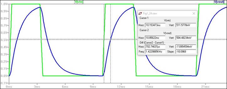
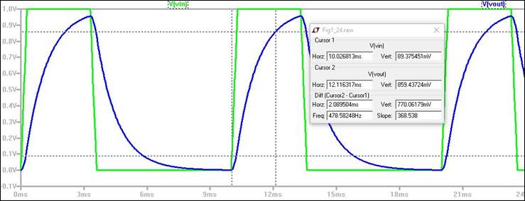
Fig. 1.24 Delay
Time
Fig. 1.24 Rise Time
Experimental Values
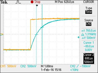
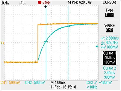
In the above oscilloscope capture, the time delay was captured at 50%
of peak output at approximately 760 µs as shown in the image on the left. The rise time
was captured between 10% and 90% peak output at approximately 2.36ms as shown
in the image on the right. These values fall within the simulation and
theoretical values previously obtained.
The table below displays the values measured in experiment three.
The measured values all fall within close range of each other.
|
Fig 1.21 |
|
|
|
Simulation |
703µ |
2.09m |
|
Theoretical |
700 µ |
2.20m |
|
Experimental
|
760 µ |
2.36m |
Conclusion
The experiments
performed in Laboratory One offered the opportunity to review basic RC
circuits, to practice LT Spice simulations and to compare the values obtained via
different methods of analysis, specifically experimentation, hand calculation
and simulation. The laboratory results also demonstrated the variances that may
occur within the different methods of analysis due to different means of
measuring inherent in each technique.
Return to
Monahan Lab Report Directory
Return to EE 420L
Spring 2016 Student Directory