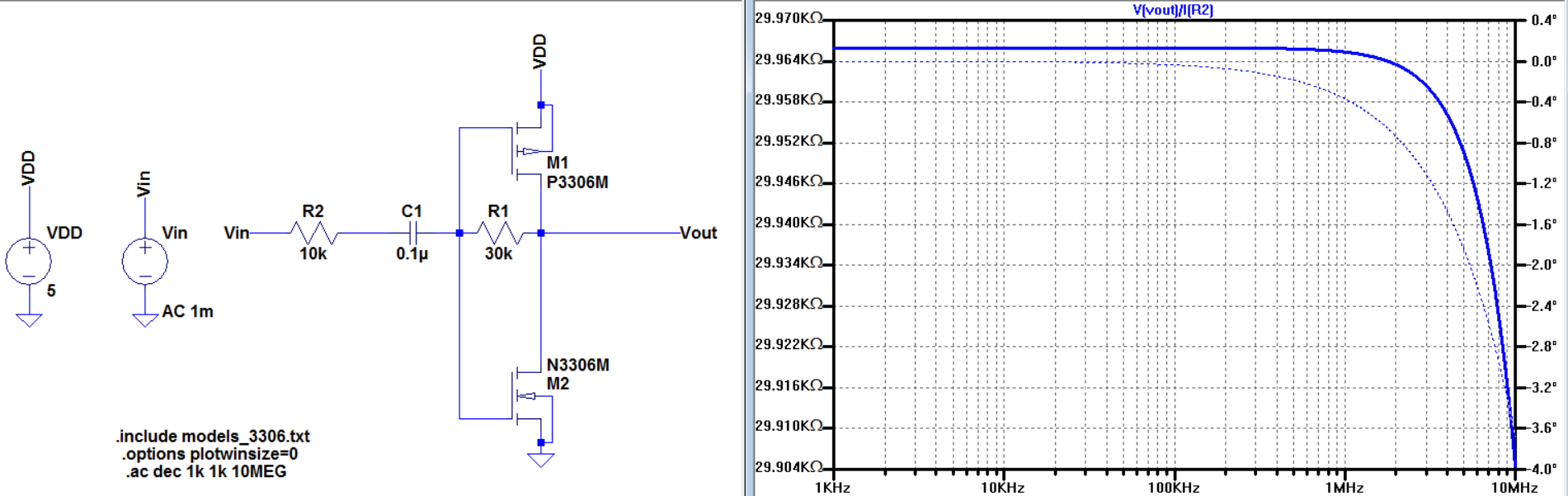
Above is the initial design for our amplifier. We used a AC simulation
to show the gain between the input and output voltages. Since this is
an transimpedance amplifier a voltage output over a current input will
result in a resistance gain. For the above design we use the 30k
resistor for Rf in the push pull topology, Rf is our gain resistor,
since the goal is to have 30k gain we should set Rf to be 30k ohms.
What matters isn't the 30k gain, the purpose of this amplifier is to
drive up a voltage using a small input current. The above design works
fine without any load. However from what we learned from lab 6 and lab 7.
The push-pull amplifier will result in a lower gain swing on an actual
board, and we can lose gain from driving a load. To rectify this we
need to do two things, we lower the input current so that we can both
avoid saturation and fully realize the gain, next we can add in a
source-follower in ensure that the circuit can drive loads without
sacrificing it's gain.
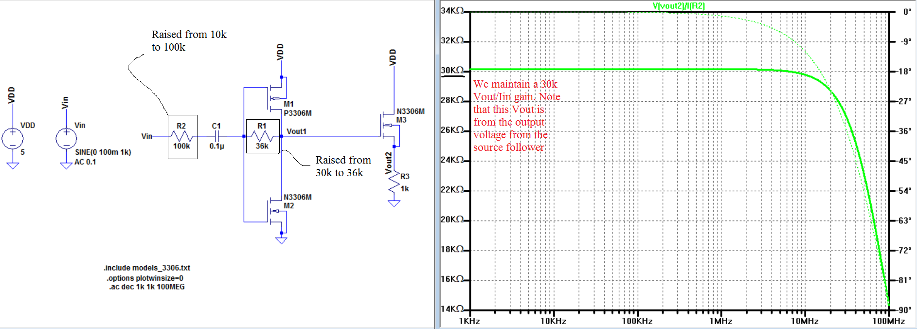
Above is the push-pull design that feeds into a source follower. To lower our input current we raised the input resistance by a factor of 10, this is so that we lower the risk of having the output swing of our amplifier from saturating. Next the Rf resistance was raised, this is due to the source follower not ideally having a gain of 1. We know this from lab 6 , where in the NMOS calculations we have Vout/Vin = 1k/(1k+1/gmn) = 0.95 V/V for the voltage gain. In order to ensure that the overall gain is 30k we raise Rf to be slightly larger. Since we are expecting the gain to drop in the NMOS stage by raising the resistor Rf we can expect the output gain of the nmos to drop down to 30k, 36k was given due through sweeping Rf.
Due to the limitations of our measuring equipment, transient simulations where used so that we will have a better understanding of what voltages we should expect to occur from the experimental results.
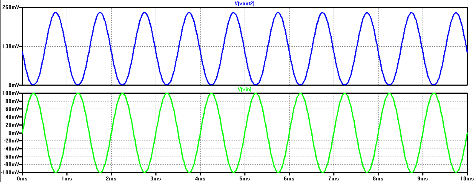
From what the simulation tells us we should expect an output gain with
a DC bias of about 100mV, and an 180 degree phase shift. The phase
shift is not unusual as this is the result from the push-pull circuit.
We know from lab 6
that a push-pull amplifier will have and 180 degree phase shift and we
also know that source follower circuit will not adjust the phase shift
again, this will result in an total phase shift of 180 degrees. Another
thing to not is that the AC amplitidue for both Vin and Vout is nearly
identical, Vout has a swing nearing 100mV
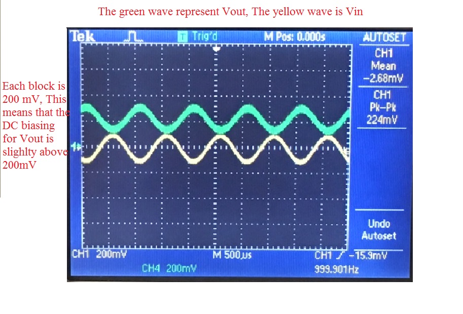
For the measure wave we see two things that match the simulation
result. First the phase for the output is correct. Second the swing for
the output nearly matches the input. However there is one thing wrong
with this wave form, we find that the DC bias is around 200 mV while
with the simulation we should have expected this DC voltage to be around 100 mV. This could result in our calculated gain to no match the simulated gain.
Next we try to measure the input current of the amplifier. Due to the limitations of our equipment this will be difficult, however we can measure the current by using a small test resistor and measuring the voltage difference across it.
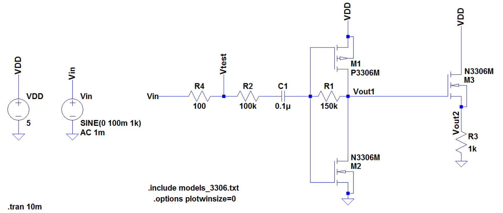
Next we try to measure the input current of the amplifier. Due to the limitations of our equipment this will be difficult, however we can measure the current by using a small test resistor and measuring the voltage difference across it.
Above shows the circuit used to measure the input current. We use a
small test resistor in the input node, by doing this we create a new
voltage labed Vtest. By measuring the Vin and Vtest with our probes we
can calculate the input current of the circuit. I in = Vin - Vtest / 100
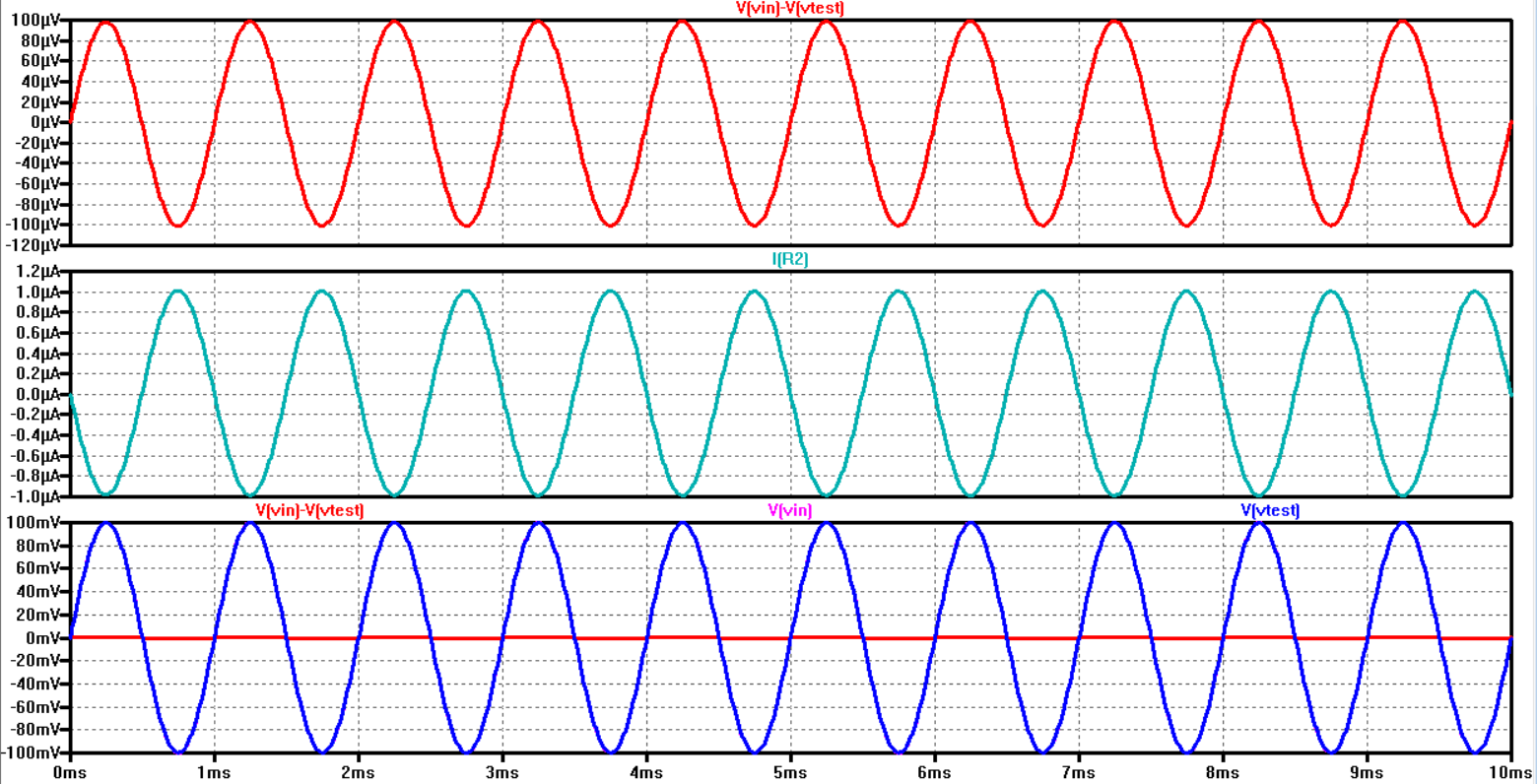
To showcase that this will work a transiant simulation was used. The
first two plots shows the current I in and the voltage difference
between Vin and Vout. We see that the voltage difference between these
two voltages is about 100 uV, divide that voltage by the 100 Ohm
resistor and we will have a current with a 1uA swing. The bottom graph
shows us what we should expect from the oscilloscope waveform. An 100
uV difference is incredibly small and in order to calculate the current
with these measurments, the scopes measure function will be used to
give us our numerical values.
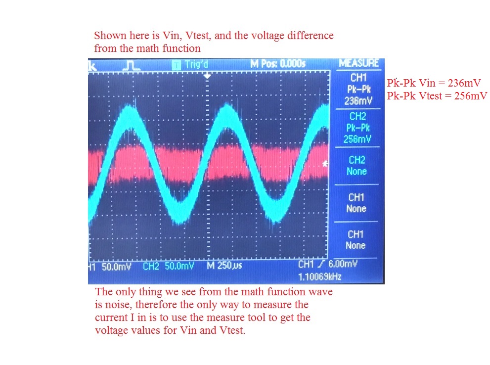
As expected from our simulations we won't be able to see much of a
swing from the voltage difference, however there is a voltage
difference from these two measurements. Vin = 236 mV and Vtest = 256
mV. Using R = 100 Ohms we have our measured input current to be 200 uA.
Now this is 200 times larger than our simulated current, however based
on the measured waveform we see that at this level of current we will
have noise. The extra amplitude for I in is likely an result from
unwanted noise signals. With the measured voltage and current we can
calculate the actual gain of the design. 200 mV / 200 uA = 1000 Ohms.
With the rather high input current we find that our overall gain for
this circuit is rather low. This is mostly due to the high input
current in our design. Another possibility as to why the calculated
gain is incorrect is due to poor methods of calculating the input
current.
Even though the gain is incorrect in our design, this circuit can still
drive and operate within and past our design contrants. We find that
despite what the load is the output voltage will remain the same, this
is due to the source-follower circuit which enables this circuit to
drive a load. This circuit can also operate at low frequencies without
losing gain, as shown in the bottom table plots.
Even though the gain wasn't correct, either due to poor measurements or biasing to avoid having a saturated swing. This circuit is a an transimpedance amplifier that can operate at a wide range of frequencies (100Hz to 10MEG), and can drive multiple varying loads (1k to 10k and 0.1u to 1u). This circuit also works using only VDD = 5. Raising VDD to a higher voltage would have increased our range for an output swing which would enable the input current to be larger, which would have resulted in easier methods in measuring the current. However raising VDD that high would result in drawing a lot of power particularly across the push pull circuit, which would generate a lot of heat.
| Driving a capacitive load (10p) |  | 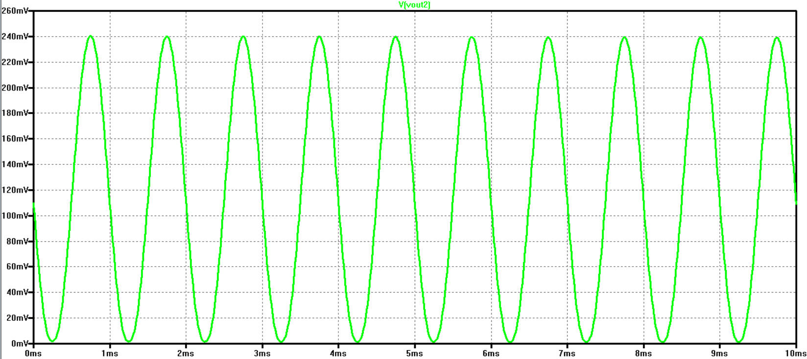 |
| Driving a resistive load (10k) | 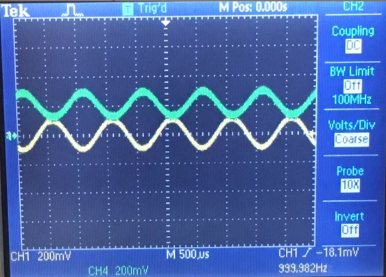 | 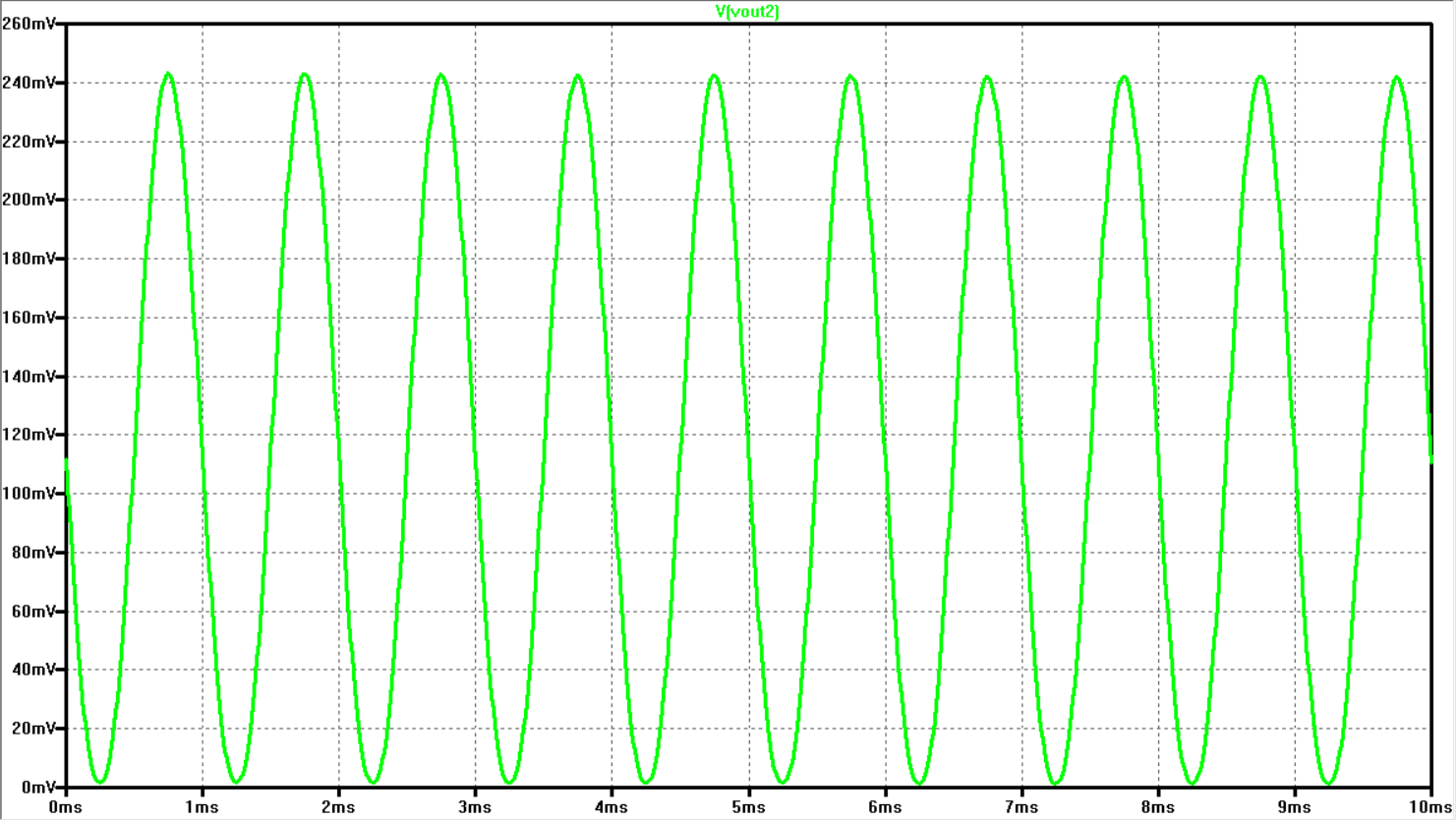 |
| Frequency = 100 Hz | 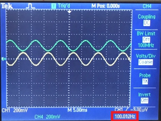 | 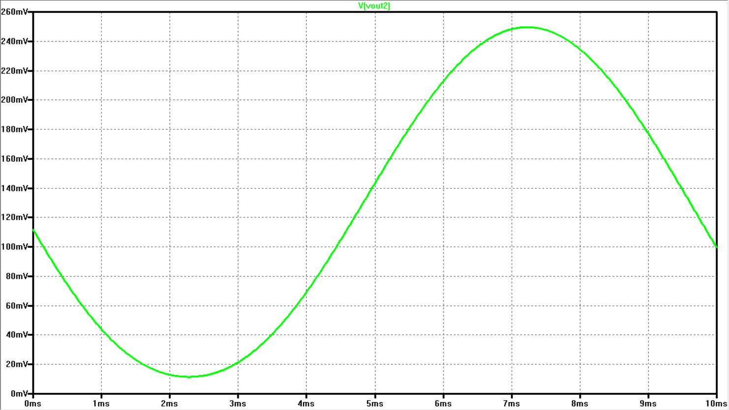 |
Even though the gain wasn't correct, either due to poor measurements or biasing to avoid having a saturated swing. This circuit is a an transimpedance amplifier that can operate at a wide range of frequencies (100Hz to 10MEG), and can drive multiple varying loads (1k to 10k and 0.1u to 1u). This circuit also works using only VDD = 5. Raising VDD to a higher voltage would have increased our range for an output swing which would enable the input current to be larger, which would have resulted in easier methods in measuring the current. However raising VDD that high would result in drawing a lot of power particularly across the push pull circuit, which would generate a lot of heat.