Lab 6 - EE420L
Authored
by Rodolfo Gutierrez
gutie284@unlv.nevada.edu
3/28/2016
Single-stage transistor amplifiers
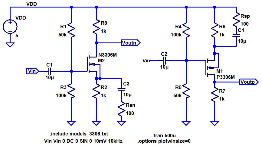
- Below are schematics for NMOS and PMOS source followers amplifiers (also known as common-drain amplifiers).
- In your lab report discuss the operation of these circuits.
The source follower circuit works by utalizing the voltage divider
equation Vout = Vin Rout / Rout + 1/gm. So the gain in these circuits
are dependant on gm and Rout. We can manually pick any value for Rout,
however the gm is dependant on the DC biasing, primarily the value for
Rin.- Simulate the operation of these amplifiers.
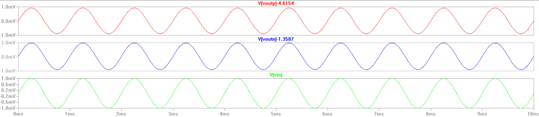
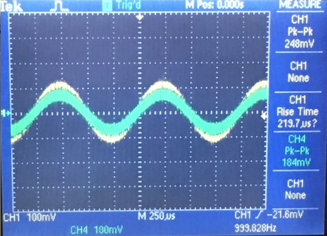
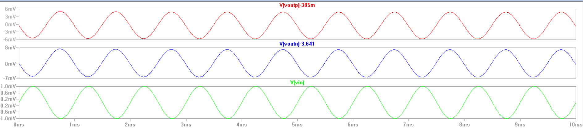
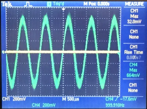
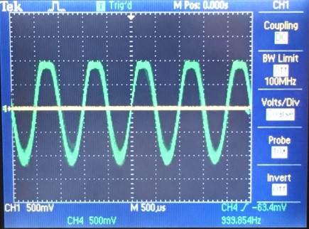
Here we see that the gain for the nmos and pmos circuits is a little less than 1V/V with no phase shift.
-
Hand calculate, and then verify your hand calculations with
experimentation and simulations, the gains and the input and output
resistances ensuring that your test signals are at a high enough
frequency that the caps have negligible impedance but not so high that
the gain is dropping off.
-
If you build this circuit using electrolitic capacitors, assuming the
input AC signal swings around ground, put the "+" terminal of the cap
on the gate of the MOSFET. Please indicate, in your lab report, that
you understand why the capacitor is connected this way.
The capacitor is connected to the gate of the mosfet due to the DC
voltage becoming much larger than the AC input, the positive terminal
of the electrolitic capacitor must be connected to the higher potential
voltage.
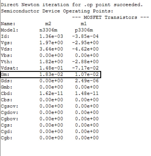
For the hand calculations we need to know gmn and gmp which can be found with simulations.
NMOS
Rin = 50k//100k = 33k Ohms
Rout = 1k//1/gmn where gmn = 18.3 m from the simulation
Rout = 51.813 Ohms
Vout/Vin = 1k/(1k+1/gmn) = 0.95 V/V which is about 1
PMOS
Rin = 100k//50k = 33k Ohms
Rout = 1k//1/gmp where gmp = 10.7m
Rout = 85.47 Ohms
Vout/Vin = 1k / (1k + 1/gmp) = 0.9145 V/V
For the measured values we have
NMOS
Vout/Vin = Rx / (1/gm + Rx)
Where Rx is a
load resistance. If we find that the gain becomes 1/2 then we will know
that Rx = 1/gm
From our measured values Vout/Vin = 0.75 when Rx = 30.2
(Rgm + Rx)0.75 = Rx
Rgm = (Rx-0.75Rx)/0.75 = 10.0667 Ohms
gmn = 1/10.0667 = 0.0993 A/V
our thoretical value for gmn and
measured value is incredibly off. This is likely due to the differences
between a real world mosfet and a simulated mosfet, such that the
circuit needed a different value for the gate voltage to get a matching
value for gmn
Rout = 9.96 Ohms
PMOS
Rgmp = (Rx - Vout/Vin (Rx))/Vout/Vin
Vout/Vin = 0.59 at Rx = 0.91.2 Ohms
Rgmp = 63.37
1/gmp =
0.01578 A/V = 15.78 mA/V, which is near our theoretical value for
gmp
Rout = 59.6 Ohms
NMOS
| Gain with no load | Gain with load | Input Resistance |
 |  |  |
PMOS
| Gain with no load | Gain with load | Input Resistance |
 |  |  |
- In your lab report discuss, in your own words, how to measure the input resistance.
-
For measuring the input resistance add a resistor equal to the value
you calculated between the input voltage source and the amplifier.
-
Measure the peak AC current through this added resistor by taking the
difference in the peak AC voltages across the resistor (on one side is
the input voltage signal and the other side is the connection to the
amplifier's input capacitor) and then dividing by the resistor's value.
-
Measure the peak AC voltage on the input of the amplifier (the left
side of the capacitor).
-
Dividing this peak AC voltage by the peak AC current through the added
resistor is the amplifier's input resistance.
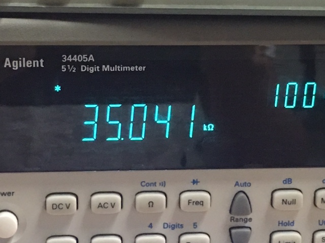
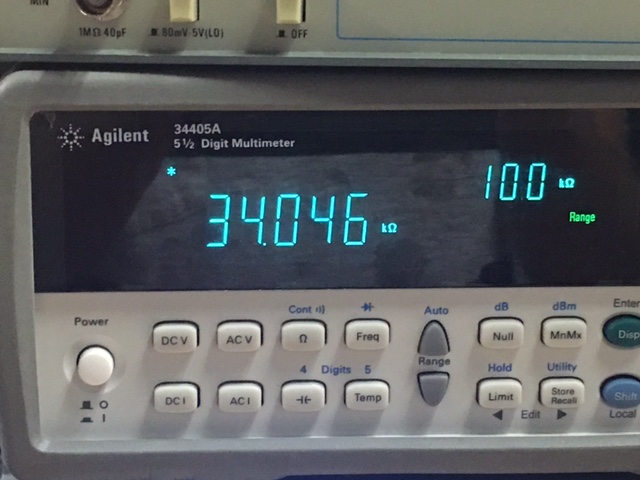
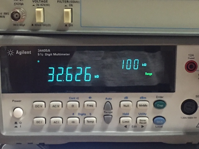
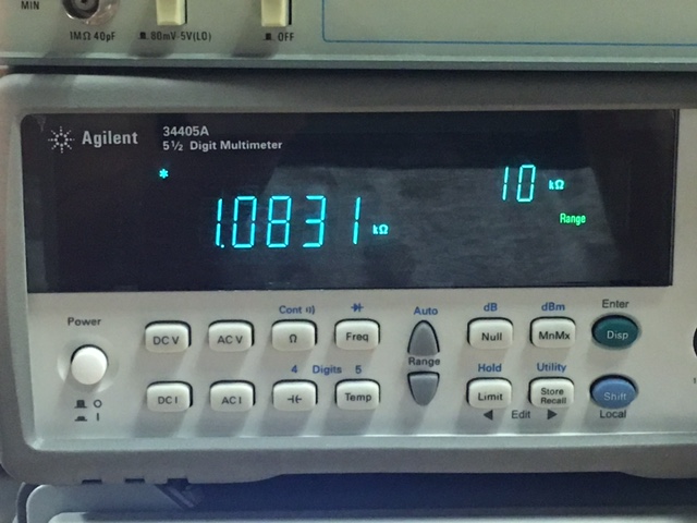
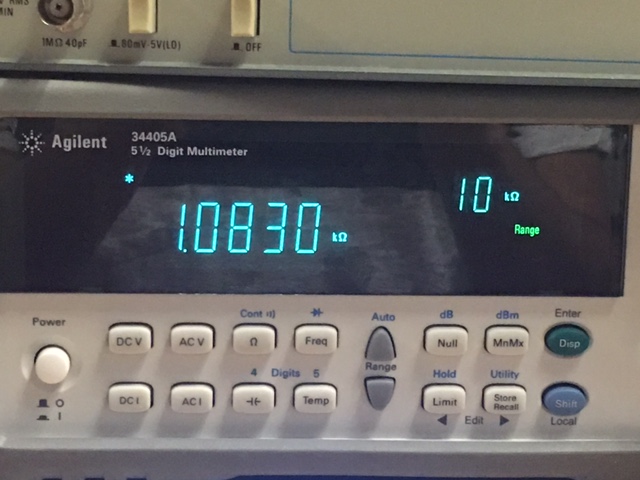
A multimeter was used to measure the resistance
between the gate of the mosfet and ground. With the above measurements
we see that Rin in both circuits is about 34k Ohms, which nearly
matches the calculated value of Rin of 33k Ohms. - Again, in your lab report discuss how to measure the output resistance.
-
For measuring the output resistance, add a resistor equal to the value
you calculated in series with a big capacitor (to avoid messing up the
biasing) from the amplifiers output to ground.
- Measure the peak AC current through this added resistor.
-
Measure the peak AC voltage (remove the DC component) on the gate of
MOSFET and the peak AC voltage on the source of the MOSFET. The
difference in these two AC voltages is the peak AC gate-source voltage
of the MOSFET.
-
Dividing this peak AC gate-source voltage by the peak AC current
through the added resistor is the amplifier's output resistance.
With the above calculations Rx was the test resistance used to measure
the Rout, by using the difference with gain we are able to calculate
the unknown value for Rout by using the known values of the gain and
test resistance.- Below are two common-source amplifiers.
- Discuss the operation of these amplifiers in your lab report including both DC and AC operation.
The common source amplifiers function a lot like an op-amp with the
inverting topology. The gain for these ampliferes is dependant on the
resistor on the drain terminal of the mosfet RD, and the parallel
combination of the two resistors connected to the source terminal
Rss//Rs. The gain equation for these circuits is Vout/Vin = -Rd/(1/gm +
Rss//Rs). Notice that the gain will be negative for a common source
amplifer, which is why its function is comparable to an op-amp with an
inverting topology.- Hand calculate the gains and the input/output resistances.
- How does the source resistance, Rsn or Rsp, influence the gain.
Rsn and Rsp are in a relate to the gain in
Vout/Vin = -Rd/(1/gm + Rss//Rs)
So large values for Rs will become negligible as the parallel
combinations will replace large Rs values with Rss, however if Rs is
smaller than Rss then Rss will become negligible and Rs will have a
larger effect on the gain. So for high gain it is better to set Rs to
be as small as possible.
For the hand calculations we have
NMOS
Vout/Vin = -Rd/(1/gm + Rss//Rs) = -1k / (1/18.3m + (1k//100) = -6.87 V/V
Rout = Rd = 1k Ohms
Rin = 50k//100k = 33k Ohms
PMOS
Vout/Vin = -Rd/(1/gm + Rss//Rs) = -1k / 90.01 + 1/10.7m = -5.423 V/V
Rout = 1k Ohms
Rin = 100k//50k = 33k Ohms- Again compare your hand calculations to simulation and experimental results.
For the simulations
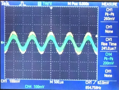
With these simulations we see that a common source amplifer will have
an negative gain, for the amplitudes we see that the gain in the nmos
is around 7 V/V and for the pmos the gain is about 5 V/V. These
simulations closely match the hand calculations
In the measured values we have
NMOS
| Gain | Input Resistance | Output Resistance |
 |  |  |
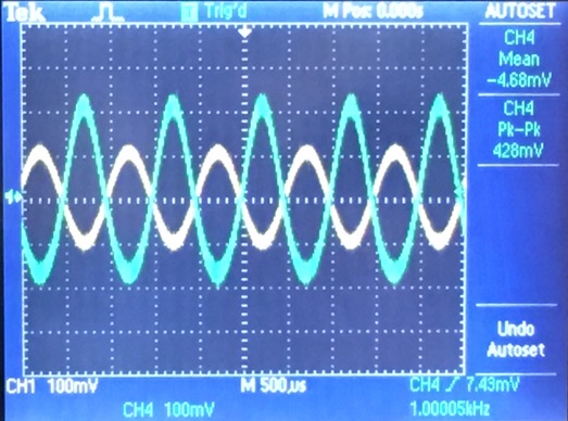
Here
we see that the gain is 6 V/V with a 180 degree phase shift. Which
is off from our theoretical calculation by about 1V.
PMOS
| Gain | Input Resistance | Output Resistance |
 | | |
Here
the gain for the pmos equivalent circuit is about 2 V/V, which is
incredibly off of the theoretical value for the gain, this is likely
due to incorrect biasing.
- Below are two common-gate amplifiers.
- Discuss the operation of these amplifiers in your lab report including both DC and AC operation.
For the common gate amplifier we find that the gain functions simularly
with an op-amp that has an non-inverting topology. The gain for these
circuit is Vout/Vin = Rd/(1/gm + Rs), which nearly mirrors the gain in
the common-source topology, however we can expect the gain to be
positive and Rs is no longered influenced by the resistor connected to
the source terminal. - Hand calculate the gains and the input/output resistances.
- How does the source resistance, Rsn or Rsp, influence the gain.
For the gain we have Vout/Vin = Rd/(1/gm + Rs), Since Rs is no longer
in a parallel combination its size can greatly influence the gain. If
Rs is too large we will reduce the size of the gain, to insure that the
gain will be high we need to take not that Rd must be larger than Rs.
NMOS
Vout/Vin = Rd/(1/gm + Rs) = 1k/(100 + 1/18.3m) = 6.466 V/V
Rout = Rd = 1k Ohms
Rin = Rs + 1/gm = 154.64 Ohms
PMOS
Vout/Vin = 1k/(100 + 1/10.7m) = 5.17 V/V
Rout = 1k Ohms
Rin = 154.64 Ohms- Again compare your hand calculations to simulation and experimental result
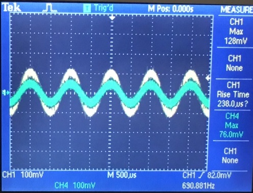
For the simulations we have
In the Common-Gate case we see that there will be no phase shift. For
the nmos the gain is about 6 V/V, and for the pmos we see that the gain
is about 5 V/V. These simulated gains do match with our hand calculated
gains.
With the measurements we have
NMOS| Gain | Output Resistance |
 |  |
PMOS
| Gain | Output Resistance |
 | |
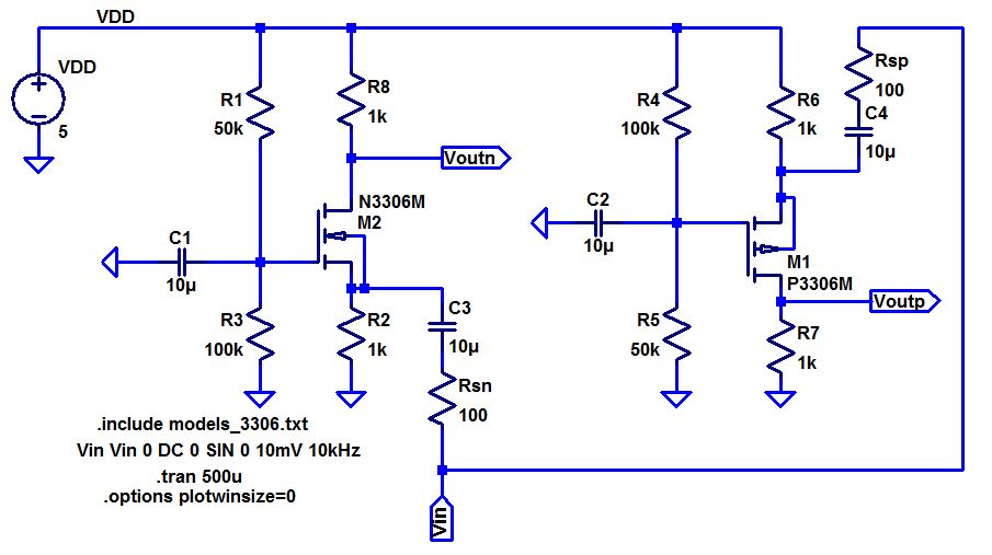
- Below is a push-pull amplifier.
- Discuss the operation of this amplifier in your lab report including both DC and AC operation.
- Hand calculate the gain of this amplifier.
Vout = Rf * (gmp + gmn)*Vin
Vout/Vin = Rf * (gmp + gmn) = 100k (10.7m + 18.3m) = 2900 V/V- Do you expect this amplifier to be good at sourcing/sinking current? Why or why not?
This circuit is good at both sourcing and sinking
current. With the PMOS the circuit can source the current, and with the
NMOS the current will sink. - What happens to the gain if the 100k resistor is replaced with a 510k resistor? Why?
We should expect the gain to increase by an factor of 5.1
Vout/Vin = 510k (10.7m + 18.3m) = 14800 V/V- Again compare your hand calculations to simulation and experimental results.
-
Note that the gain of this amplifier is large so the output may
saturate at VDD and Ground. To avoid this saturation you can reduce the
AC input voltage using a voltage divider.
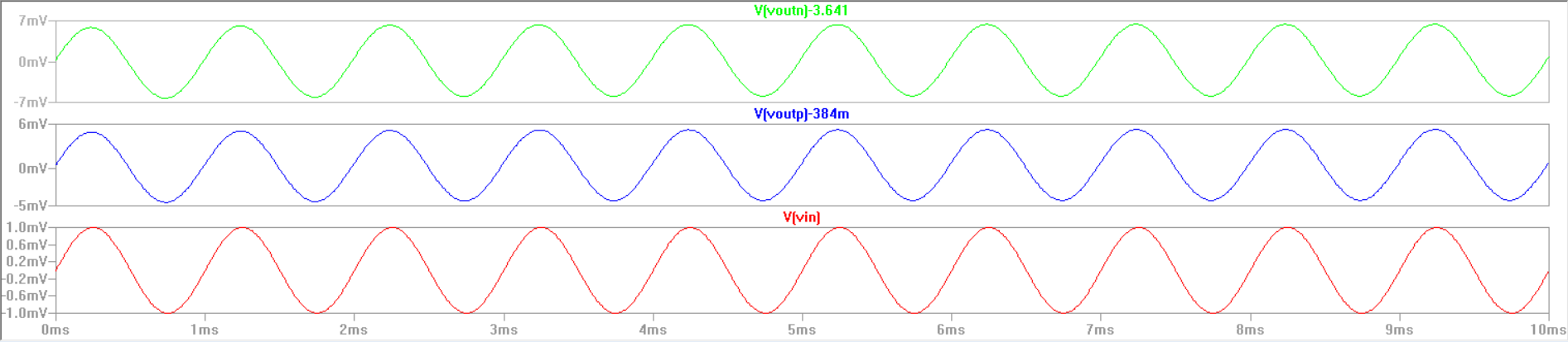
For the simulations we have
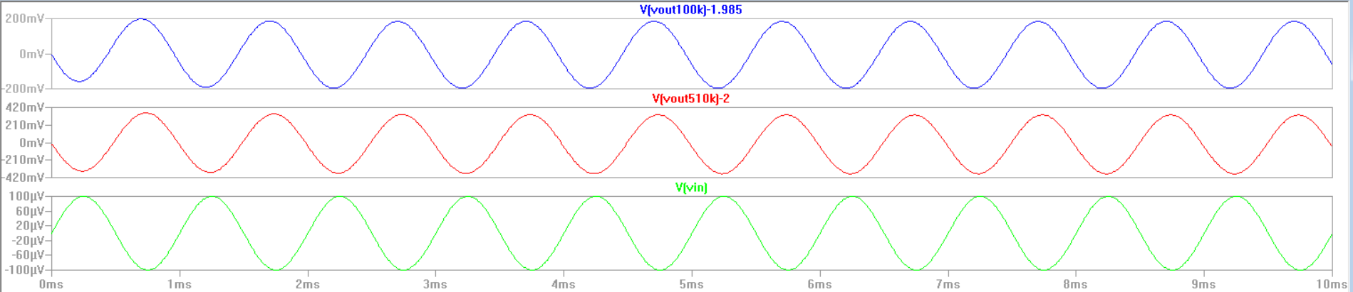
In order to avoid
saturation a input voltage of 0.1 mV was used. When Rf=100k we
find that the gain is about 2000 V/V , which is lower than our
calculated gain. When Rf=510k we see that the gain becomes about 4000
V/V. For the 510k resistor we see that the gain only increased by a
factor of 2 and not 5.1, meaning that there is some sort of limit with
increasing the gain.
| Rf = 100k | Rf = 510k |
 |  |
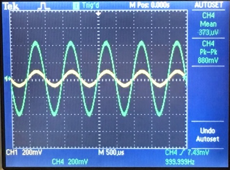
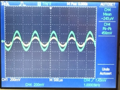
Now we see that the push-pull amplifier is capable of large
gains, with Rf = 100k we have a gain of 120 V/V for a 10mV input, this
is a lot lower than the hand calculated gains, this is probably due to
the limitations of physical mosfets in preforming huge gains. For the
510k case we had saturations when using a 10mV input. At a 1mV input we
still see a small amount of amplitude, but the gain here is around 1000
V/V. Though the calculated gain was alot larger we still find that
increasing Rf will have a huge effect on gain. Another possibility for
why the gain is small with the measured case is that our gm values for
the mosfets are smaller than the simulated and calculated cases.
Return