Lab Project - EE 420L
Authored
by Shada Sharif,
sharifs@unlv.nevada.edu
8 May 2015
Lab Project Description:
- Building a BGR (bandgap voltage reference) using the CD4007.pdf as well as using the level=1 model from lab 8
Lab Project Requirements:
- using
as many diodes, resistors, and capacitors as needed, along with two
CD4007 chips from the same production lot (see date code on the top of
chip) to ensure current mirrors are possible, design and build a
bandgap voltage reference (BGR). Your report, in html, should detail
your design considerations, simulation results (using the models you
generated in lab 8), and measured results showing the BGR's performance (how the reference voltage changes with VDD).
_____________________________________________________________________________________________________________________________________________________
- BGR - bandgap voltage references are used to generate a fixed voltage, Vref,
that does not vary with the power supply of the circuit. This means
that as VDD, power supply, increase or decrease the reference voltage
stays constant at a fixed potential. BGRs are also sometimes
independent of temperature meaning the reference voltage does not change with temperature.
- Designing the BGR -
- after
characterizing the CD4007 MOSFETS and having a level=1 model from lab
#8, we were able to have all the parameters needed to start the design
by simulating the circuit seen in Figure 23.27 PG.765 from the CMOS book.
- The
circuit mainly consists of a cascode current mirror using MOSFETS, but
in our design we did not cascode since it would require many of the
CD4007 chip though it would have been good practice to cascode since it
would have improved the matching of current due to a higher output
impedance.
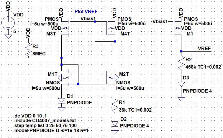
- The BGR circuit consists of two main circuits, the
Diode-Referenced Self Biasing (CTAT), and the Thermal
Voltage-Referenced Self Biasing (PTAT). When PTAT and CTAT are combined
we get the BGR. We combine these two circuits in order to have the
reference that does not vary with VDD or temperature.
- In
the design, diodes were used knowing that the current through a diode, as
it decreases with increasing temperature, causes the voltage drop across
the diode to decrease. So, in the mirrored stage of the design we see
that a diode was connected in series with a resistor. This is because,
with increase in temperature the VD
(voltage across diode) drops and the voltage across the resistor
increases, so the effects of both cancel each other and we get a voltage
that does not change with temperature.
- In the design we
also have multiple diodes connected in parallel, and it has the same
concept that was used in making a beta-multiplier that is independent
of VDD, where we have K diodes and K times more
current and we can have some voltage drop left for the resistor
connected in series with the diode. So that the voltage drop of VD1 is greater than the voltage drop across VD2.
- Moreover, since the circuit
needs a start up circuit and requires more chips to be used, we used
a very large resistor connected to VDD. The resistor does the same
thing as the start up circuit by slowing the current down until the current mirror reaches the desired state.
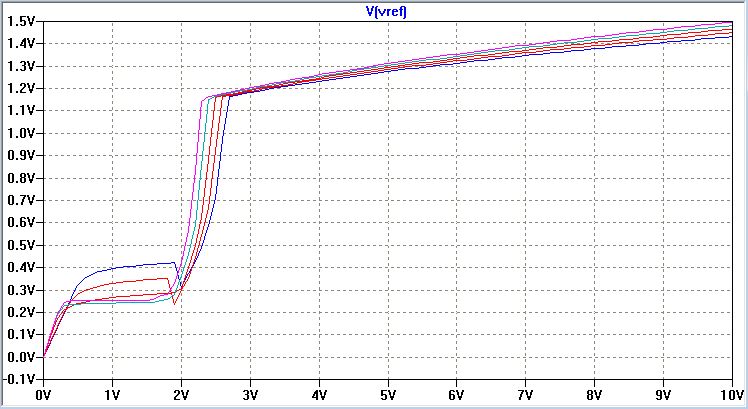
- The LTspice simulation below shows the circuit and the reference voltage as the VDD changes from 0~10 V. We notice that in the level=1 model
from lab 8 the output resistance of the MOSFETS was not included, thus
explaining why the Vref is not increasing drastically with increasing
VDD.
- Using the level=1 model
that includes other parameters about the CD4007, we see how the output
is varys more with increasing VDD than the above simulations and later
see it matches the experimental results.
- The model was found online from Link.
- In
this simulations, we see that the width and length are more reasonable
since usually for the PMOS the width of the device is bigger than that
of the NMOS due to the mobility difference.
- Calculation explaining the resistors value for the circuit above:
- This
explains why there were 4 diodes in parallel and the resistance
picked was 36k ohms and then the resistor R2 in the mirrored branch is
L*R thus 468k ohms. This ensures that the current is 1µA.
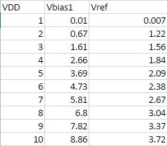
- After
having these values calculated and simulated using LTspice, we
constructed the circuit on a breadboard using a total of 3 CD4007
chips. The circuit worked fine without the start up resistor so it was
not used during the experiment. Power supply was used and varied from
0~10V, and along the variation of VDD we used a multimeter to measure
the voltage from the Vref node on the circuit. The table below shows
the recorded data during the experiment and a graph of this data was
made using excel.
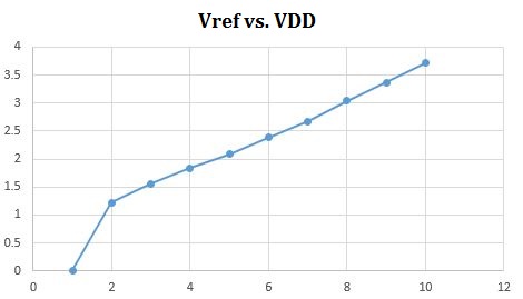
- Comparing
the experimental results to the results from the simulations we see
that the experimental Vref goes up to higher value at 10V. While
testing the simulation in LTspice, we notice that the start-up resistor
value affects the value at where Vref increases to. The higher the
resistor value the lower the voltage at 10V. So since we did not use
the start up resistor as the simulations we can say that the
experimental results are at good standing with the simulations.
- As
seen in the wave above with a 1MEG ohms resistor for start up the Vref
at 10V go almost to 3.2V while before with a 8MEG resistor it went up
to 2.3V.
- As for the change in temperature we can use ltspice by taking the deivative of Vref over the Vref voltage at VDD of 5V.
- We see that the equation for the change of Vref with temparature shows a rate of 0.885m/°C, while in the simumaltion at ~25°C the change of Vref with temperature is around 1.0m/°C.
_____________________________________________________________________________________________________________________________________________________
- Other
modification that can be done to the circuit to make the reference
voltage independent from changing VDD could be cascode as discussed
earlier. That helps increase the output impedence of the circuit and
the higher the impedence the more the output would be constant.
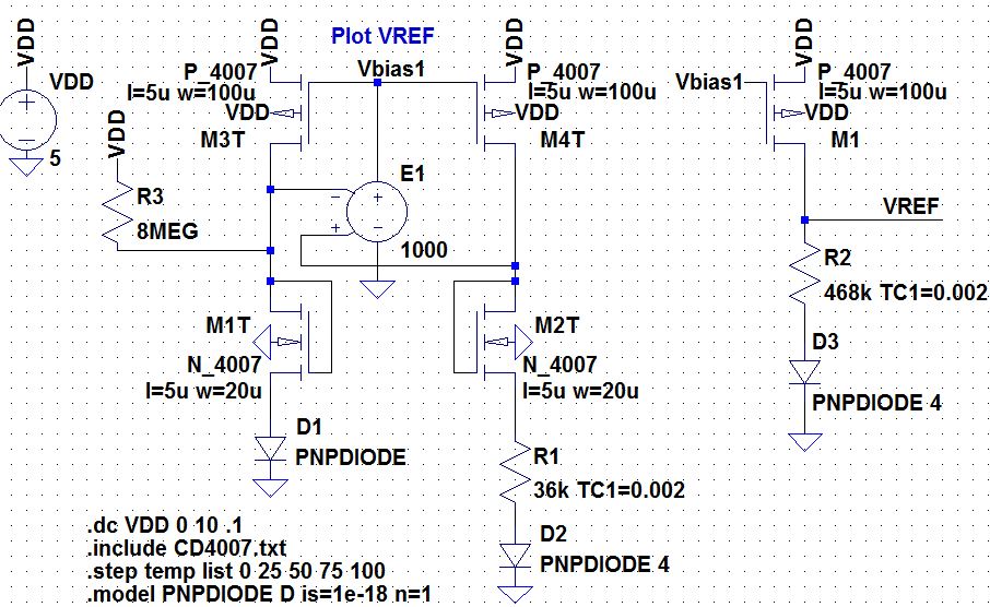
- Using
a differential amplifier would also help in making the Vref independent
of power supply variations. The amplifier would regulate the drain by feeding back the difference
between the drain voltages of M1T and M2T as well as amplify the
difference until both nodes are at the same potential. So the VSG of
M3T and M4T are the same and Iref is the same in each branch as well as
the VSD are same, all this causes ~infinite impedence and a constant
Vref output.
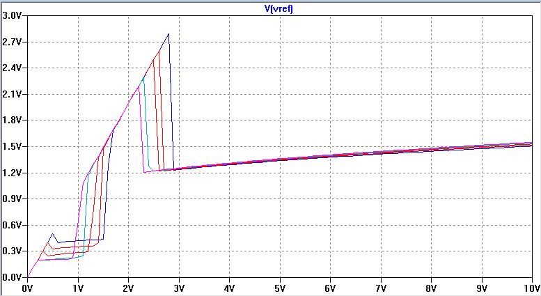
- We see that the output from 3V to 10V is not varying as
much as before the amplifier was added. As the gain of the amplifier
was increased the more constant Vref was with changing VDD. We notice
in the output wave between 1~3V there is a spike in Vref, which we were
not able to fix this problem. We thought the spike problem might be due
to the start up circuit at first but after modifying the circuit and
seeing no change the problem remained unsolved.
- We also
tried to test the amplifier added to the circuit experimentally, but
after connecting the circuit and the amplifier in the circuit, the
circuit would show a voltage at the power supply of 3V with even having
the knobs turned all the way to the left (0). So we suspect the problem
experimentally might be due to the spike seen in the wave above.
Conclusion:
The design was not perfect since as seen there were variations in Vref
as the power supply increases. To make the design better we would need
to either cascode by using more CD4007 chips, or use an amplifier after
finding out why the spike happened in the simulations.
Return to all pictures attached
Return to home directory with all other 420L labs