Lab 8 - EE 420L
Authored
by Shada Sharif,
sharifs@unlv.nevada.edu
17 April 2015
Pre-lab work:
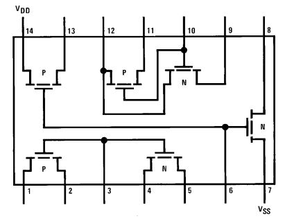
- Review the datasheet for the CD4007.pdf CMOS transistor array.
- Know that NMOS bodies are tied to pin 7 (VSS, generally the lowest potential in the circuit, say ground)
- Bodies of the PMOS are tied to pin 14 (VDD, generally the highest potential in the circuit, say + 5V).
Las Description:
- This
lab was about characterizing the NMOS and PMOS transistor CD4007, and
through the parameters found we create a Level=1 LTspice models that
can be used in simulations.
Lab report should include:
- NMOS and PMOS wave forms that were found experimentally.
- calculations and answers for the parameters VTO, GAMMA, KPn/p, and TOX.
- LTspice simulations using the Level=1 model.
- scope pictures of the inverter delay tested.
- The delay of the inverted tested in simulations.
_____________________________________________________________________________________________________________________________________________________
Experiment #1
In
this lab we characterize the transistors in the CD4007 and generate
SPICE Level=1 models. Assuming that the MOSFETs will be used in the
design of circuits powered by a single +5 V power supply.
In the experiments done to generate the plots we used two methods:
- One
method was using the scope XY feature and for the voltage that was
varied we used a function generator to generate a sawtooth wave by
taking a triangle wave and changing the duty cycle. Doing so enabled us
to have a sawtooth wave varied in the range desired. Since using the
scope we cant measure the current on the XY, we used a small resistor
100 ohms and measured the voltage across it (this was the Y-axis) and
to get the current we simply divide the voltage at a chosen point by
the resistance value. The X-axis here was the varied voltage.
- The other
method was the simpler one that is to use a power supply and vary the
voltage manually and testing the current directly with a ammeter that
is placed in series with the terminal desired (for the NMOS the ammeter
was placed on the drain, while the PMOS the ammeter was placed on the
source).
The first experiments were about generating plots for the NMOS device:
- ID v. VGS (0 < VGS < 3 V) with VDS = 3 V
For the first plot shown above, the body was grounded and the source had the resistor connected to it, as for the drain it was at a 3V potential and the gate voltage is the one that was varied.
- ID v. VDS (0 < VDS < 5 V) for VGS varying from 1 to 5 V in 1 V step
- ID v. VGS (0 < VGS < 5 V) with VDS = 5 V for VSB varying from 0 to 3 V in 1 V steps.
In
this part of the experiment since the body is being varied as well,
looking at the layout of the CD4007 shown below, we treated pin 7 (Vss)
as the body of the NMOS.


In
this part of experiment we used a different lab (350) that had function
generators that would only go up to %80 duty cycle since they were old.
Due to this, the sawtooth wave was not perfect and error was introduced
to the circuit which can be seen in the waves above. Changing the
potential of the body affects the threshold voltage. As Vsb increases
that is by increasing the potential of the source, the threshold
voltage increases and causes the current to start to decrease because
in the range the VGS is varied the device will not reach the threshold
voltage required to start conducting current.
Now plots for the PMOS device:
- ID v. VSG (0 < VSG < 3 V) with VSD = 3 V
This time the ammeter and a power supply was used to measure the current while varying VSG.
- ID v. VSD (0 < VSD < 5 V) for VSG varying from 1 to 5 V in 1 V step
The
plots above do not look perfect since at the beginning more point were
taking in smaller increments due the huge jump in current at 1V so if
the measurements were taken at 1V increment the plots would look more
like they should when VDS is varied in a mosfet.
- ID v. VSG (0 < VSG < 5 V) with VSD = 5 V for VBS varying from 0 to 3 V in 1 V steps.
Again
here we see the same idea as in the NMOS where varying the VBS changes
the threshold voltage, but here it can be seen better where the blue
plot is when VBS=0V we see that we get the most amount of current and
as VBS is increasing line in VBS=3V the yellow cure is seen to have the
smallest amount of current.
_____________________________________________________________________________________________________________________________________________________
Experiment #2
This experiment consisted mostly of calculations using informations/data from the plots generated in experiment #1.
Given:
Find:
C'ox=Cox/(L*W)=5pF/(500um*5um)=2 mF/m
TOX=Eox/C'ox=8.85e-12*3.97/(2e-3)=1.757e-8 , where Eox=Eo*Er
For NMOS:
VTO=1.0V, from the plots
GAMMA=(change in VTO)/(change in VSB)=0.8
ID=½KPN*(W/L)(VGS-VTO)^2
, solving for KPN and picking a certain VGS and the ID at that point we
find KPN=(2*300u)/(100*(2-1)^2)=6u
For PMOS:
VTO=1.7V
GAMMA=0.3
KPP=(2*155u)/(100*(2-1.7)^2)=4u
_____________________________________________________________________________________________________________________________________________________
Experiment #3
Using the parameters from experiment #2 in CD4007_models


We
notice that the NMOS waves match the experimental results while the
PMOS is a little off so we fix it by changing the parameters
accordingly.
_____________________________________________________________________________________________________________________________________________________
Experiment #4
Using the circuit shown below, we measured the delay.


So from the scope, using the measure feature we measure the delay to be 50 ns.
_____________________________________________________________________________________________________________________________________________________
Experiment #5
Simulation of experiment #4 shown below


Conclusion:
This
las taught us how to create a level=1 Spice list which is something
very useful for the future. In this experiment it would have been more
accurate and easier to use an ammeter to find the waves instead of
using a scope.
Return to all pictures attached
Return to home directory with all other 420L labs