Bad Circuit
Design 7 - Not Controlling the Current in the Output Stage
This
topic is also discussed in the book on pages 817-820 but, again, it’s such a
common mistake we discuss
it
again here.
The
unity-gain frequency of an op-amp is given by fun = gm1/2pCc where gm1 is the transconductance of the
input
diff-pair and Cc is the
value of the compensation capacitance. We know that the fT of the MOSFETs
should
be much larger than fun
(say > 10 times). We also know that the selection of the fT sets the overdrive
voltages,
Vovn
and Vovp
(Eq. [9.55]). Finally, we know that we don’t fiddle with the devices’ overdrive
voltages
with the exception of modest changes to the diff-pair (say an increase in
widths up to 4) to increase
gm1.
Having a design with varying fTs because we’ve fiddled with the W and
L is low quality (one of the
devices
will be “the weakest link” and slow
down the design.)
So,
how do we increase the speed of an op-amp? (Yes, this is also discussed in the
book. See, for example,
the
bold important on page 903.) The
answer is that we reduce Cc
and increase (modestly as discussed
above)
gm1. It’s that
simple. Ultimately, neglecting f2
(the pole associated with the output of the op-amp), we
are
limited by the biasing that sets the devices’ fT.
Assuming
the fT of the MOSFETs is
large then what limits the value of fun?
Answer: f2. As we push out
fun we
also
have to push out f2 (see
Eq. [24.24]). So how do we push out f2?
Well, if we could reduce the load
capacitance
that would help but, of course, the load generally isn’t a value the op-amp
designer can control.
So,
to answer the question, we push out f2
by increasing gm2
(the transconductance of the output stage). We do
this
by increasing the widths of the devices used in this output stage. These
devices’ overdrive voltages remain
unchanged
(important) but their drain currents increase and thus so does gm2. This is the
practical way of
increasing
the speed of an op-amp.
So,
finally, the key thing to note is that we have to precisely control the current
in the output buffer in order to
set
gm2. There are
lots of “good” op-amp designs in the book (at least the author things so ;-).
There are also
“bad
designs” seen in Figs. 24.58 and 24.59 (below).
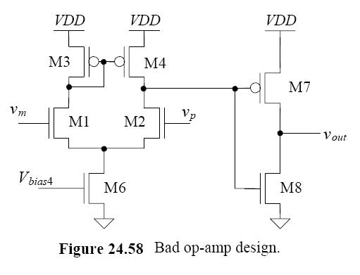
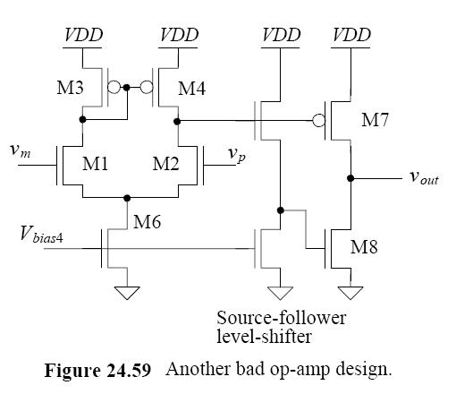
Note
that one of the places it’s easy to mess-up the biasing of an output stage is
in a 3-stage op-amp design.
See
here
for more information.