Bad Circuit
Design 1 - Dueling Current Sources
This
topic is discussed from the bottom of page 867 to page 871; however, it is such
a common problem
that
additional discussion is provided here.
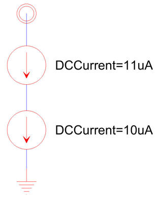
Putting
two current sources in series, as seen below, clearly isn’t possible in a real
circuit.
The
transistor(s) used to implement one of the current sources will triode to
ensure a consistent
current
flowing from power to ground.
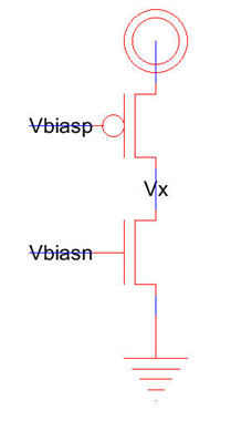
In
the transistor implementation of this circuit, below, the PMOS will triode so
that the current
flowing
in the circuit goes to 10 uA (and thus Vx will move towards VDD). It’s important to note
that
you can’t make the current flowing in the PMOS precisely equal the current
flowing in the NMOS
without
one of the devices operating in triode. Yes, once in a while it will work but
it’s not manufacturable.
Don’t
let SPICE trick you into thinking that by tweaking the length and the width of
the devices you
can
make the currents equal (yikes! ;-) and keep both devices in saturation
(always). In real circuits the
performance
will vary with process shifts, temperature, and changes in the power supply
voltage (VDD).
One
more comment before moving on, you may see this topology on the output of an
op-amp, see
Fig.
24.44 for example. If we connect both inputs of that (Fig. 24.44) op-amp to
VDD/2 the output
of
the op-amp will move towards either VDD or ground because of the issues we just
mentioned.
By
adding negative feedback around the op-amp, output back to the - input, the
“effective” bias voltages
on
the gates of MOP and MON are adjusted so that the currents in MON and MOP are
equal and the
output
voltage is set…but only by adding the feedback.
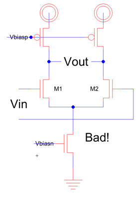
Next
consider the diff-amp with current source loads seen below. It doesn’t matter
what voltages
we
apply to the gates of M1 and M2 it’s impossible, in a real circuit, for the 20 uA currents to sum to
precisely
40 uA. Yes, once in a great while, at a specific
temperature or process run we may end up
with
a circuit that doesn’t have transistors operating in the triode region but in
any case this is bad design!
Feedback
around the circuit back to Vin will do nothing to help and your circuit will
not work!
Before
giving some transistor-level examples of this kind of bad design we should
point out that if we
employ
a circuit to measure Vout and adjust either the 40 uA
or 20 uA current sources we can get this
design
to work (the currents on the top to sum to the current on the bottom). For
fully-differential designs
this
additional circuit is called a common-mode feedback circuit.

Examples
of this problem are seen below. Besides op-amps you might see this issue in a
delay element
found
in a delay line or a voltage-controlled oscillator (see Fig. 19.57 but remove
the two gate-drain
connected
NMOS in the delay element…baddddd!)
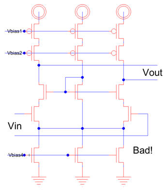
It’s
easy to show other examples, e.g., connect the gates of M5/M6 to Vbias4 instead of
to the
drains
of the PMOS/NMOS on the left side of the folded cascade stack in Fig. 22.5.
To
avoid bad design (dueling current sources) use a current mirror load (M3/M4 in
Fig. 22.6) or a
common-mode
feedback circuit (discussed from the bottom of page 867 to page 871).
Finally,
in Fig. 21.21 for example, this problem (one current source dueling with
another) is avoided by
adding
a “Big” resistor in between the gate and drain of M1. This resistor makes M1
appear, for DC, as
a
gate drain connected device (remember that for nano-CMOS there is a DC gate
current so the resistor
can’t
be too large) so M1 can sink the current sourced by M2. The “Big” capacitor
blocks the DC gate
voltage
of M1 from the AC input. Notice how we are not using voltage sources for
biasing. This (using
voltage sources for biasing) is discussed in bad design 2!
See also the following email question (others are found at this link):