PCB Designs
The top portion of this page shows pictures
of PCBs designed to test ASICs in our research group.
The bottom portion shows pictures of PCBs
designed for various personal projects.
PCB Designs for
Testing of Various ASICs
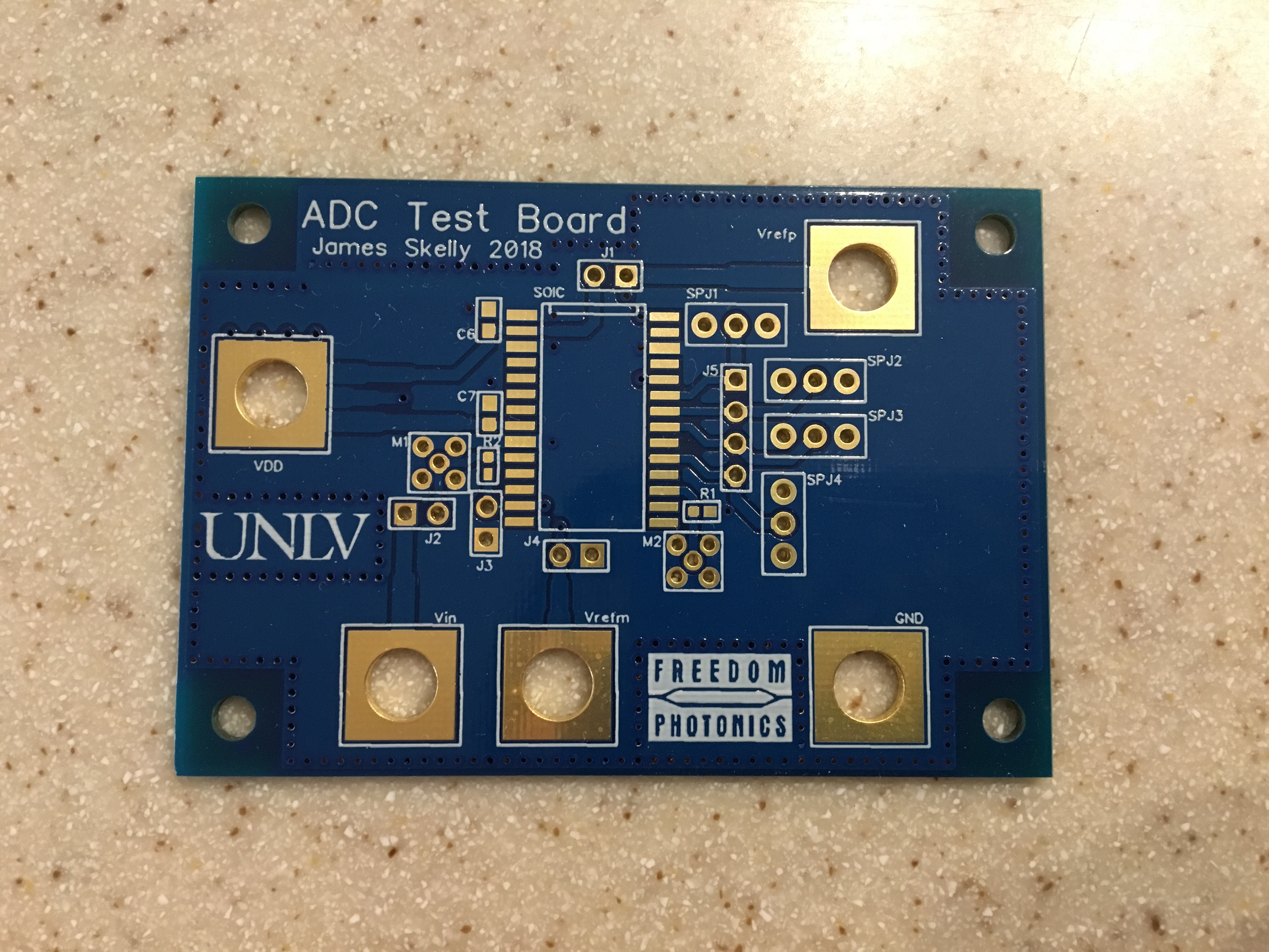
Students in Dr. Baker’s research group
design Application-Specific Integrated Circuits (ASICs) using Cadence.
Chips have been designed in the C5
Process, the AMS Process, and will soon be designed using the TowerJazz
process. The PCBs below were designed
to test these chips.
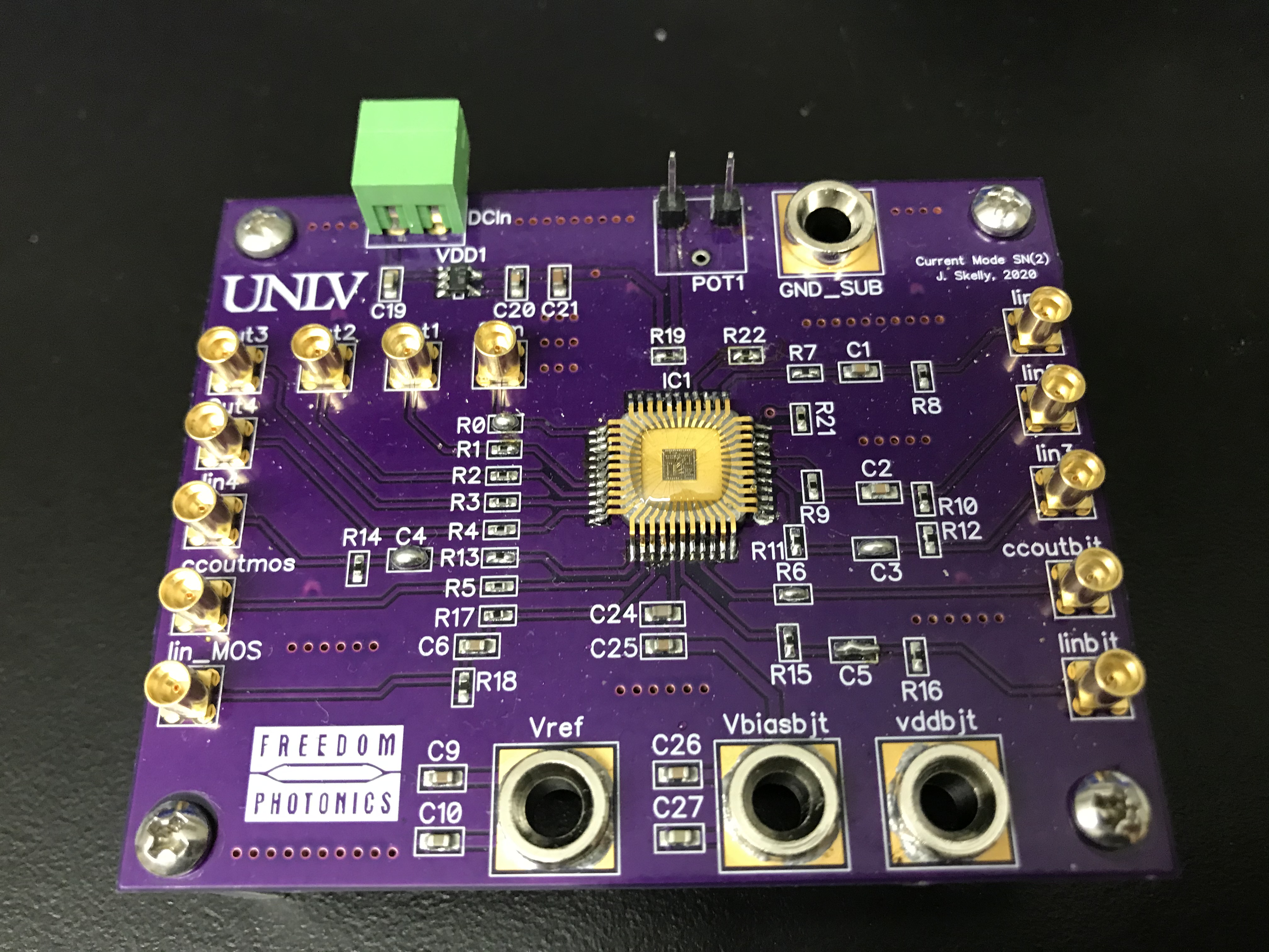
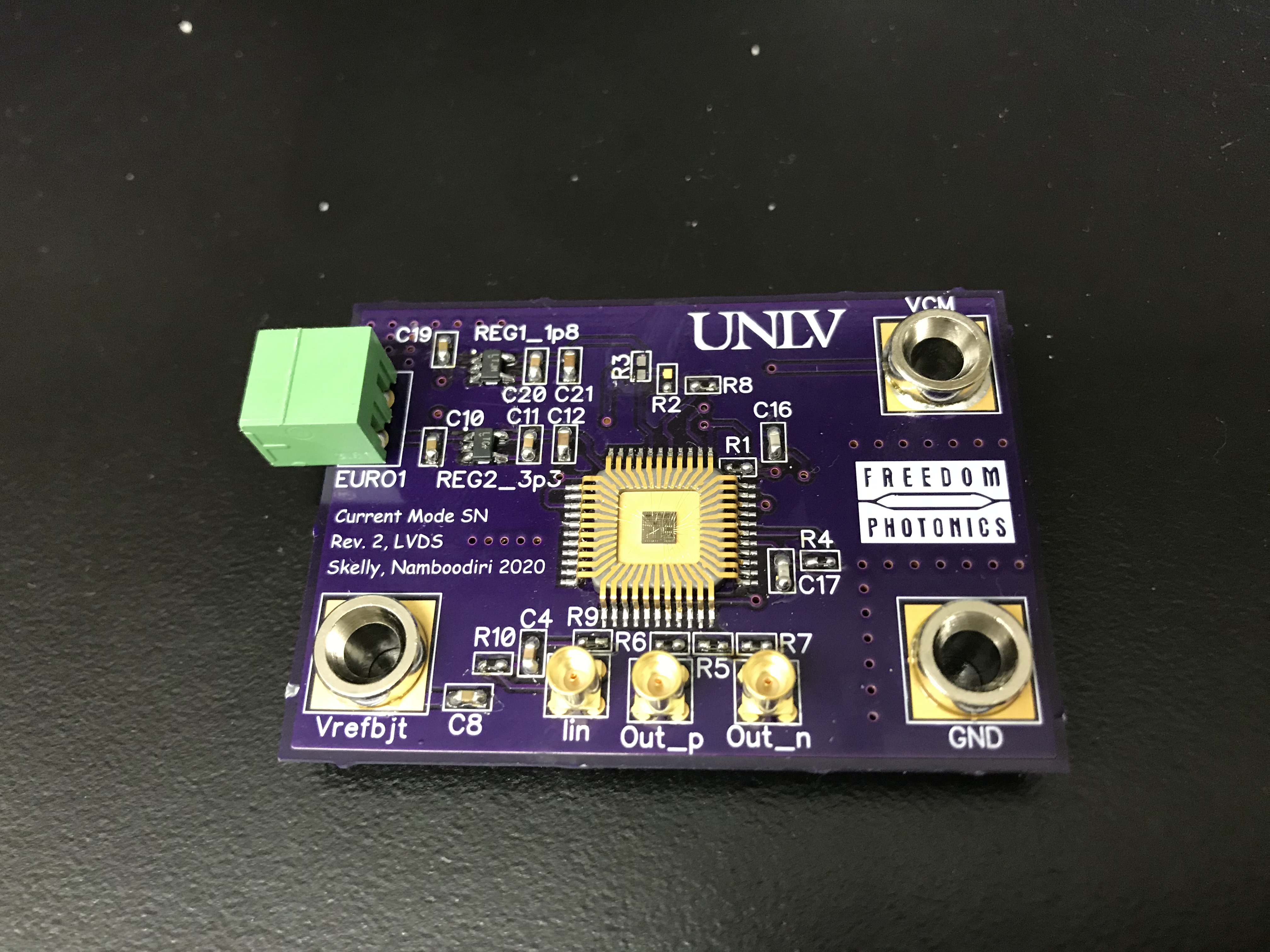
Test Boards for Sachin Namboodiri’s
Current Mode Photon Counting Circuit
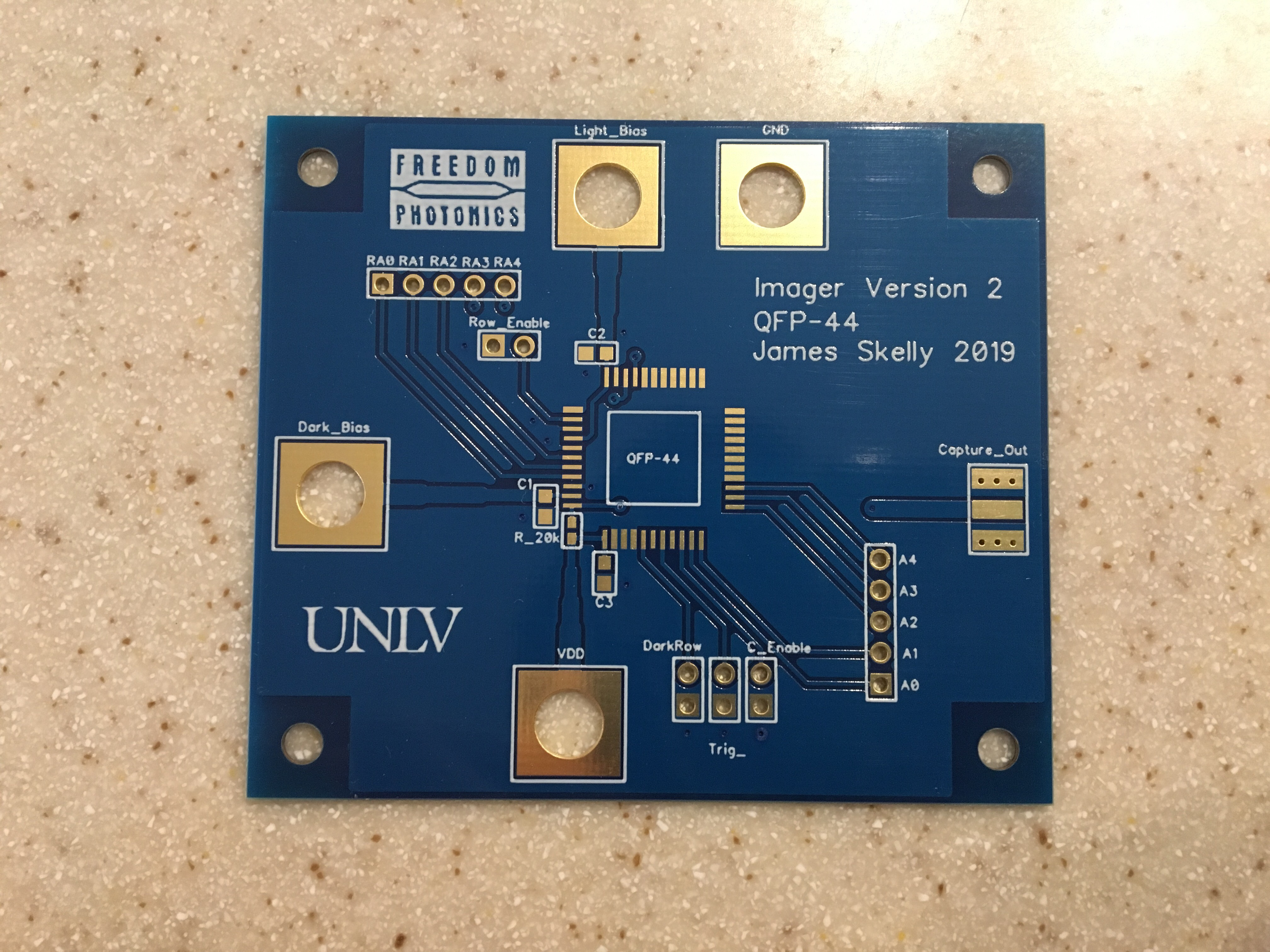
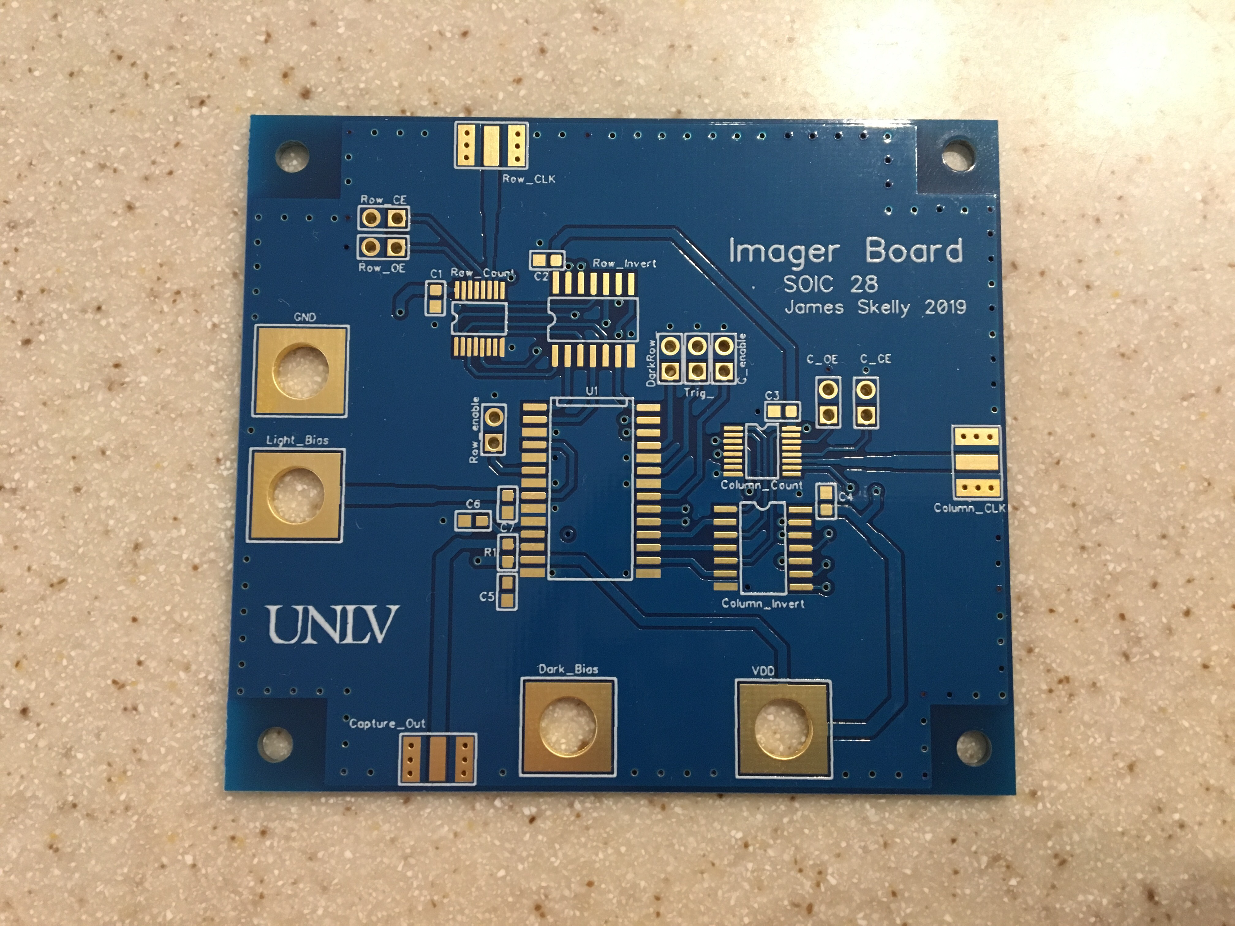
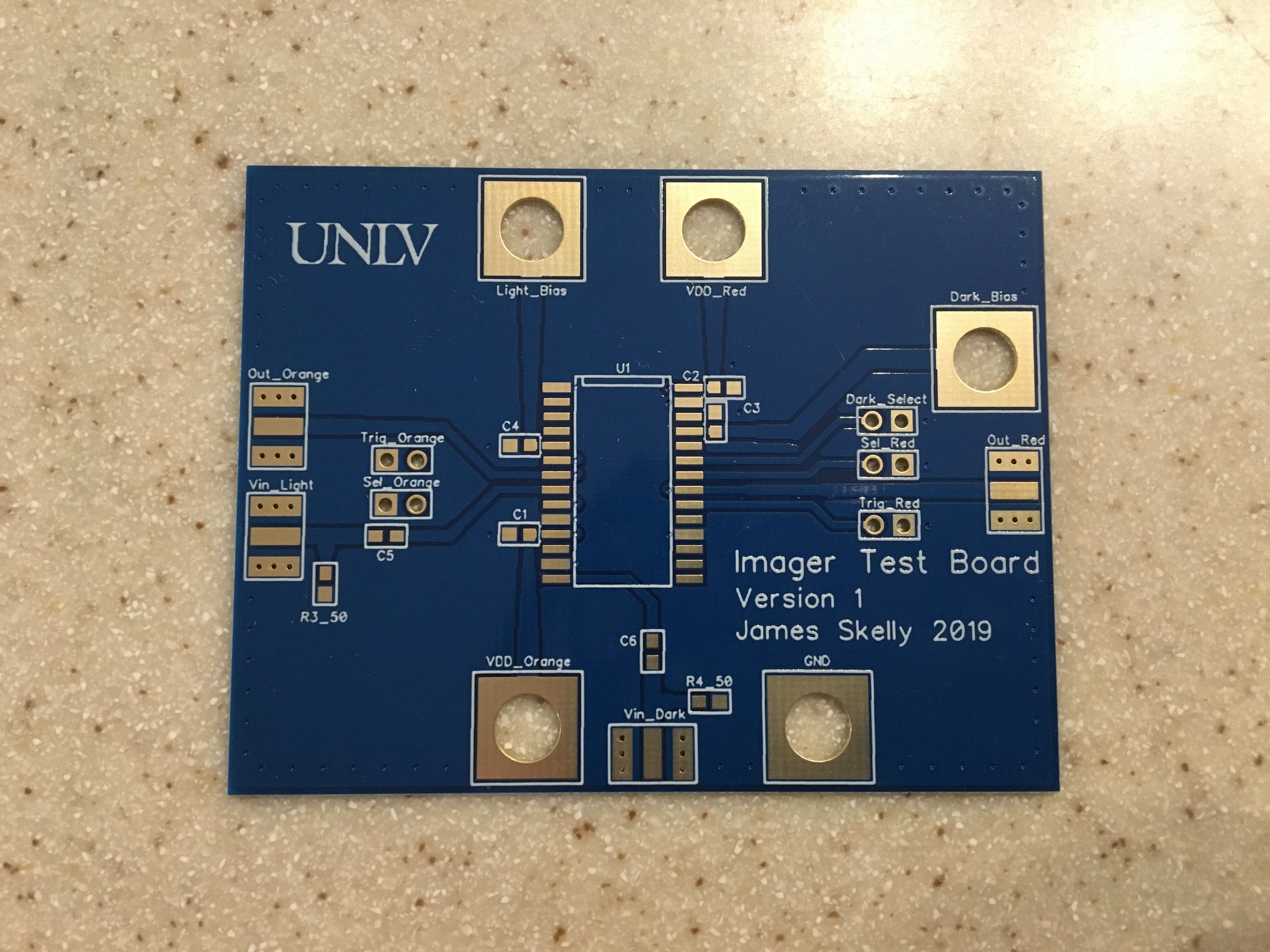
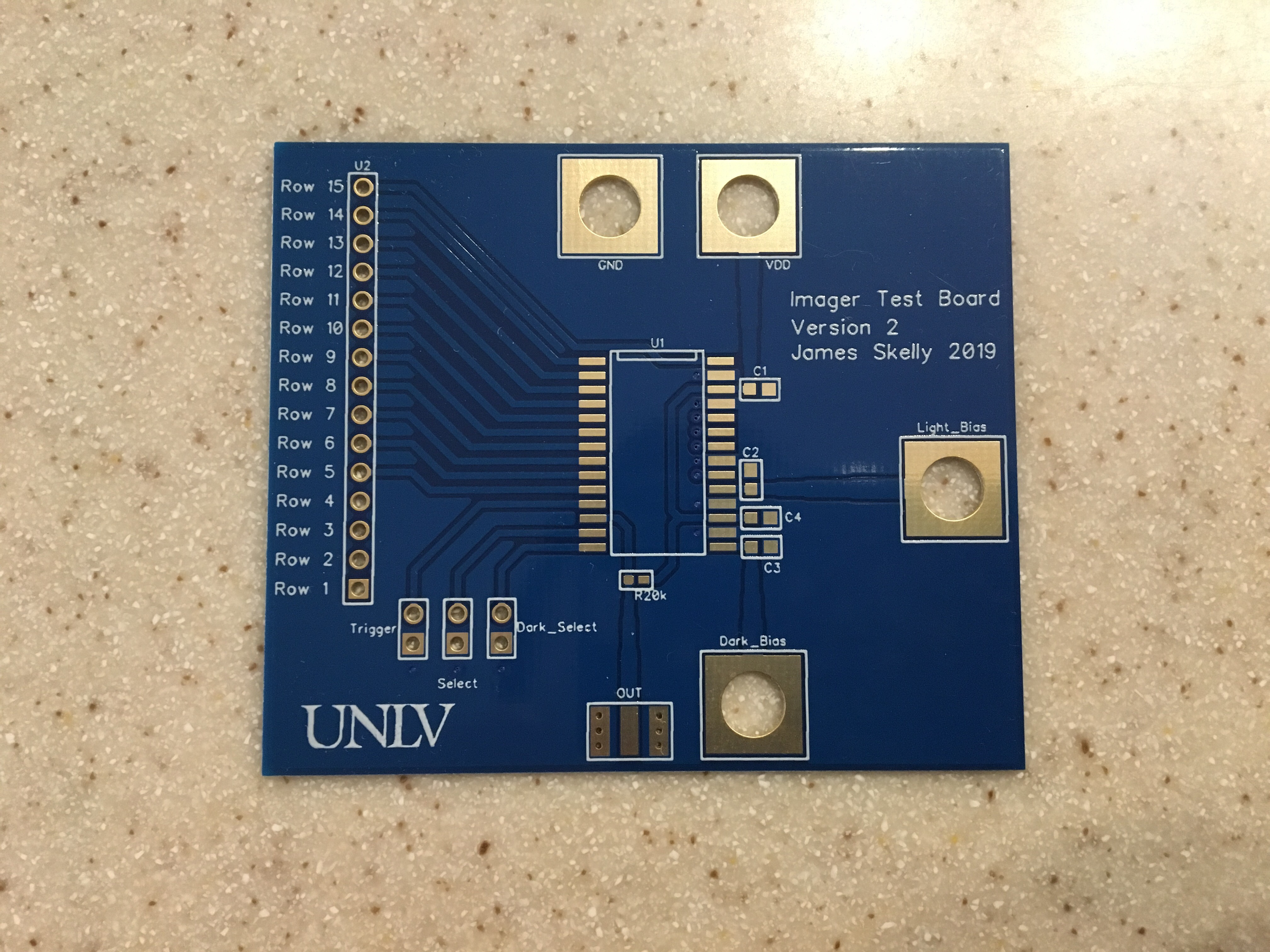
Test Boards for James Mellot’s
Imager Chip
Test Boards for Vikas Vinayaka’s
APD/SiPM Read-Out Chip
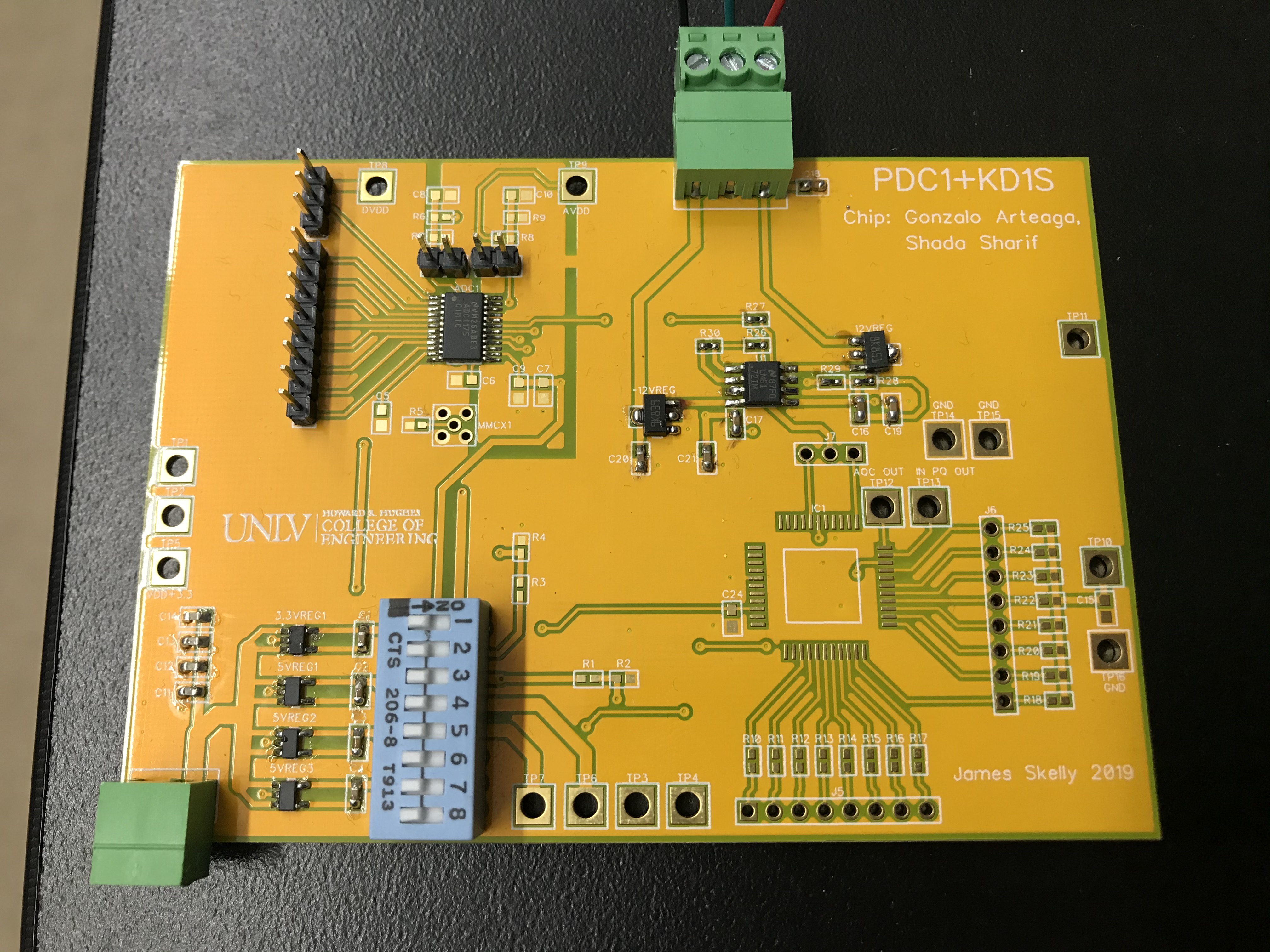
Test Boards for Gonzalo Arteaga
and Shada Sharif’s
PDC1+KD1S Chip
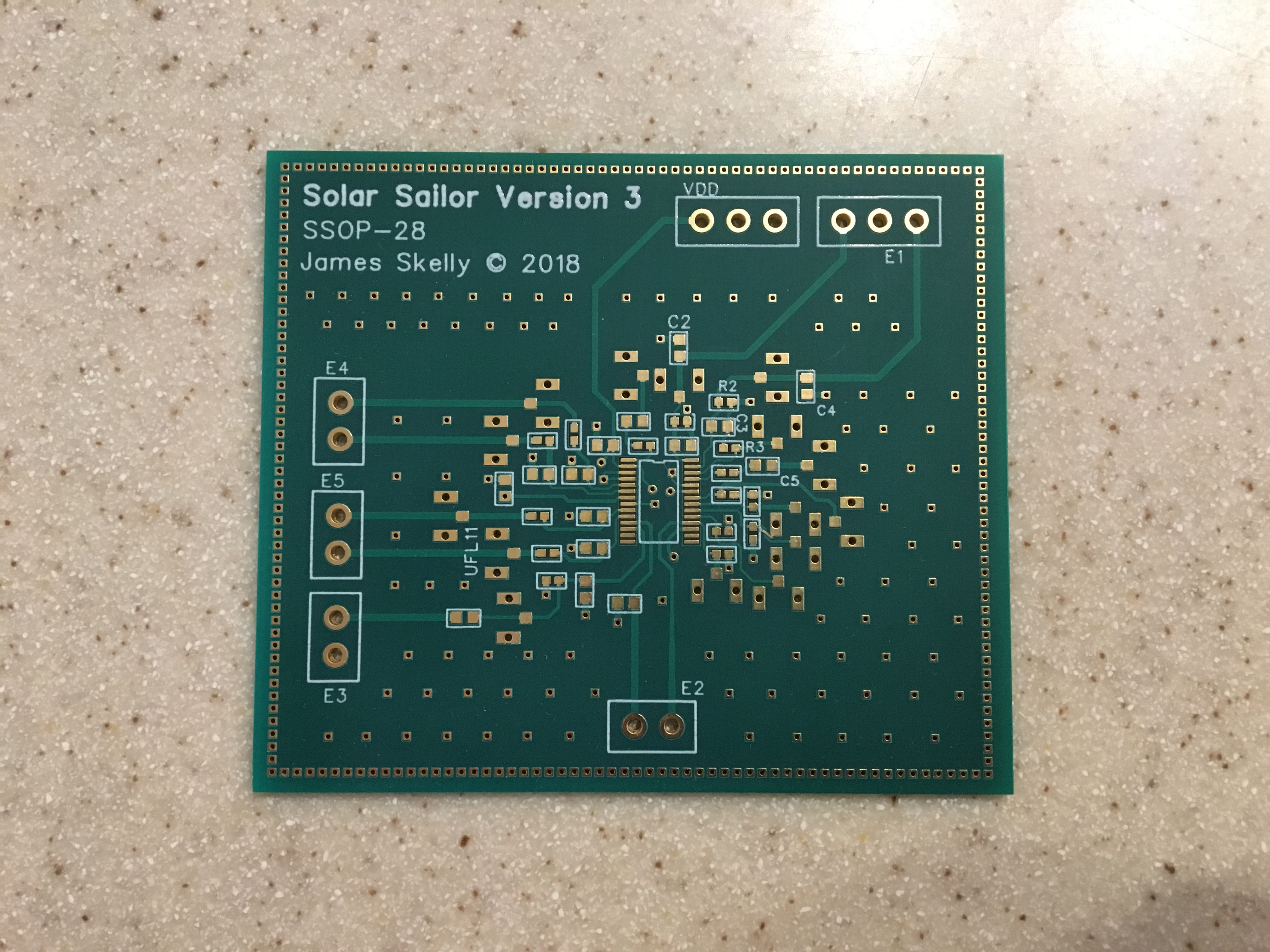
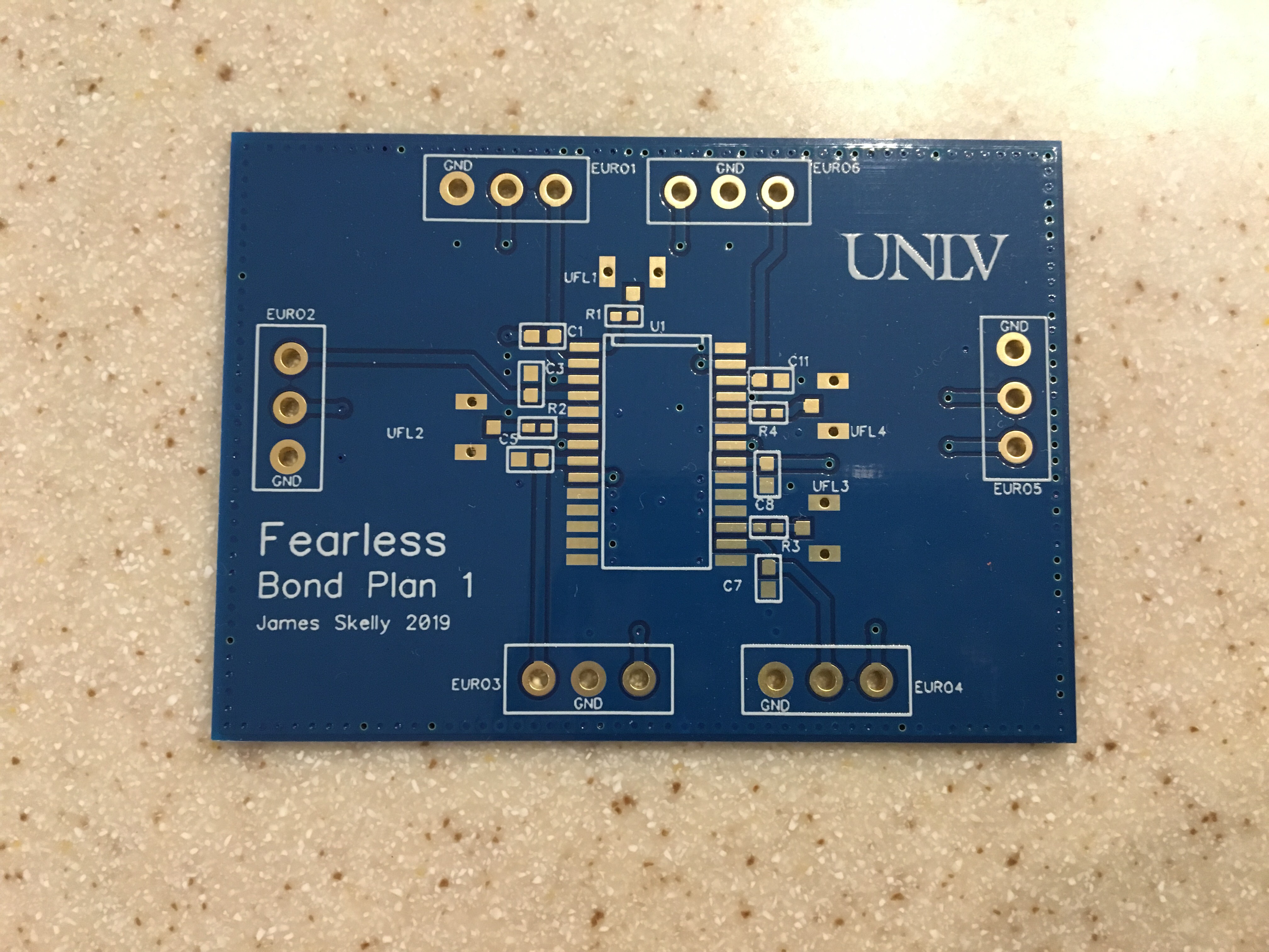
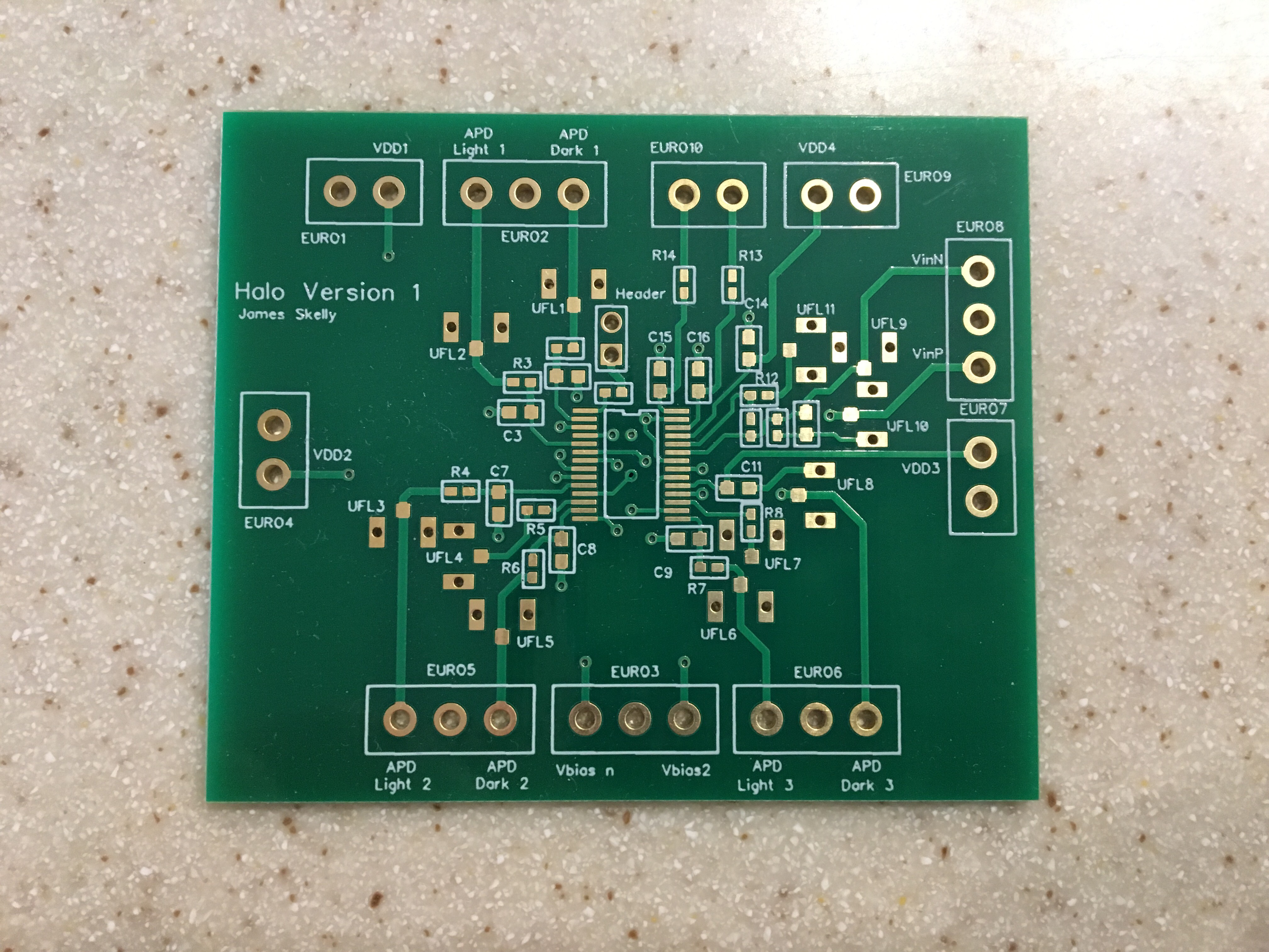
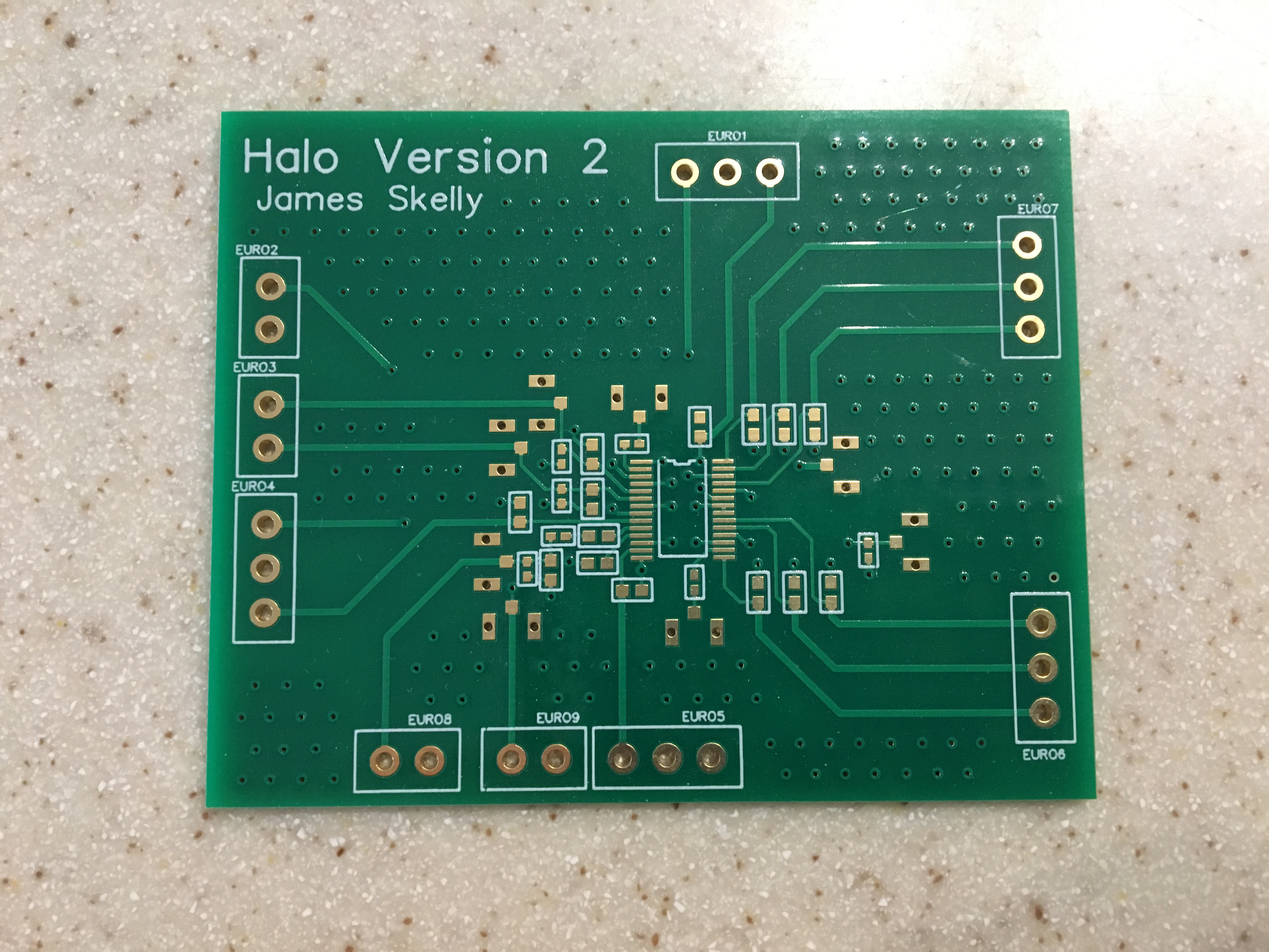
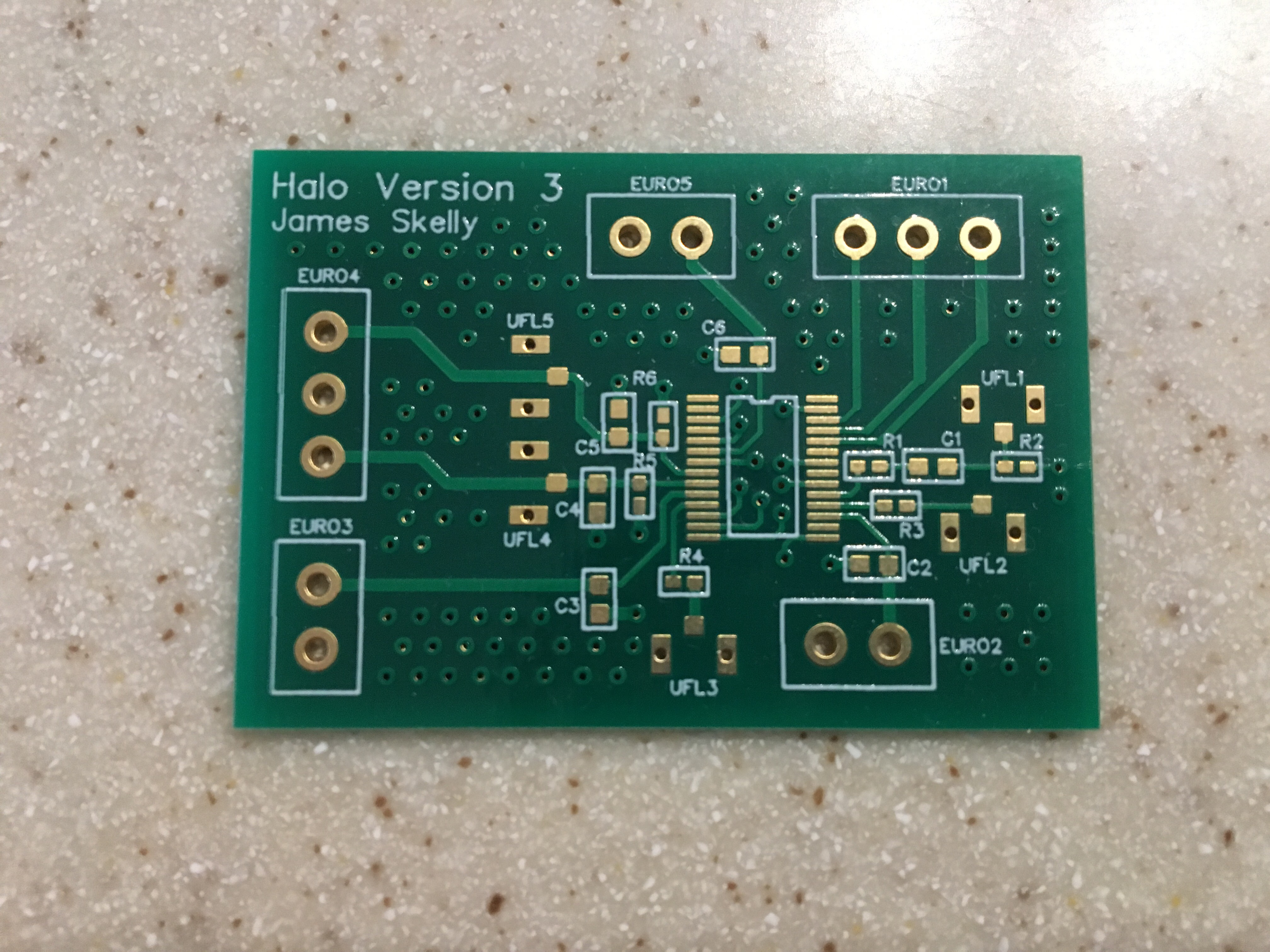
Test Boards for Angsuman Roy’s “Fearless” and “Halo”
Chips
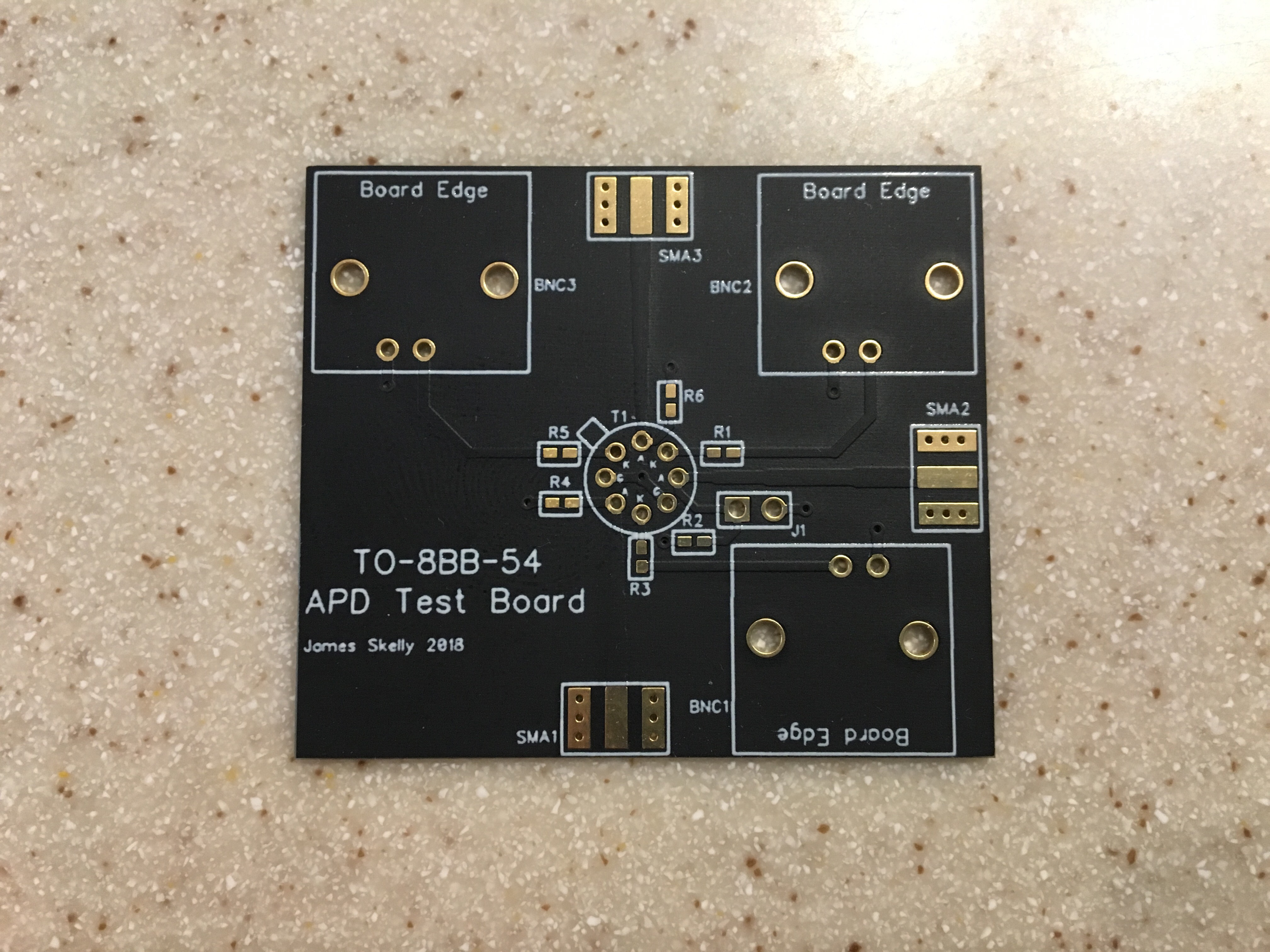
Test Boards for APD
(Avalanche Photodiode) IC Testing
PCB Designs for Personal
Projects
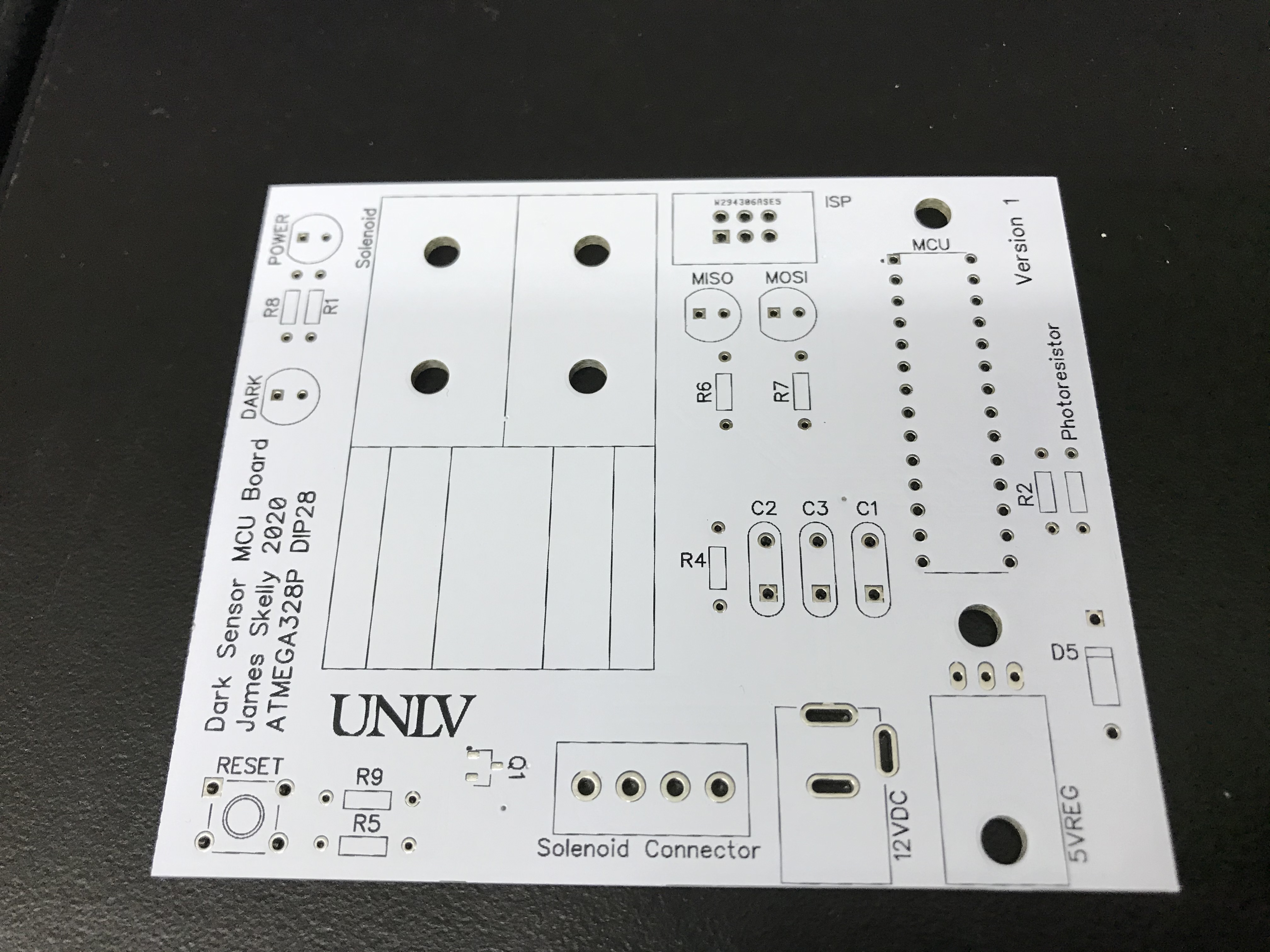
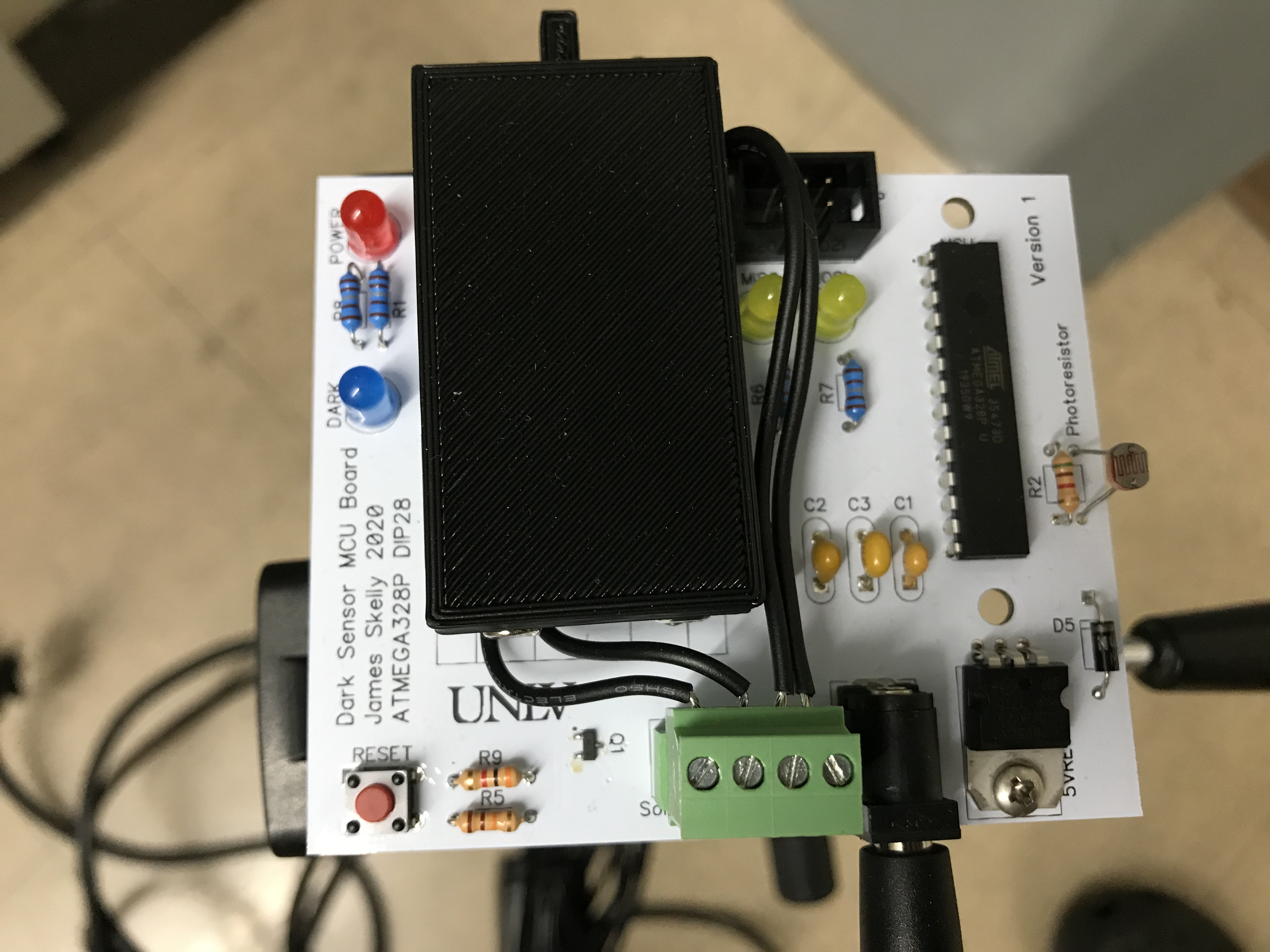
Dark Sensor PCB Using
ATmega328P Microcontroller, ISP Programming
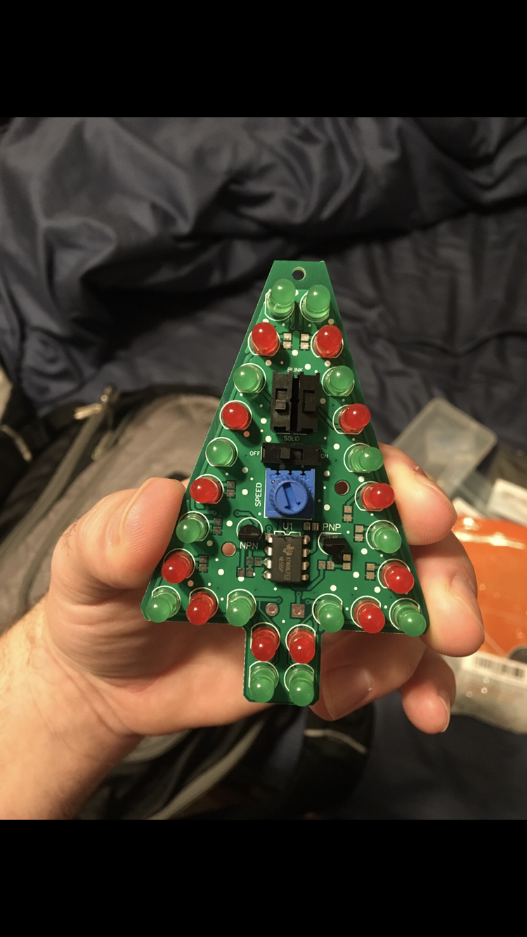
555 Timer Christmas
Tree Ornament

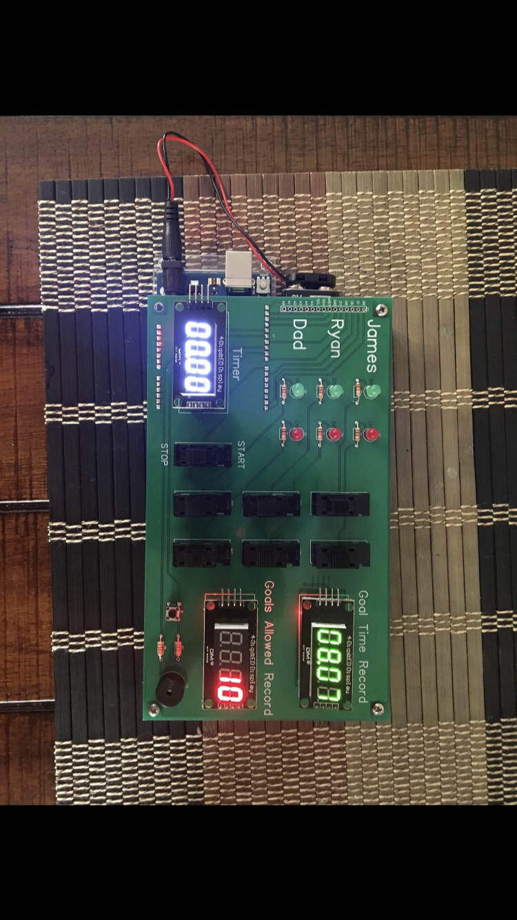
Knee Hockey Scoreboard
Arduino Shield