4-Channel Sample and Hold Chip
This chip was designed by Dr. Sachin Namboodiri and Angsuman Roy.
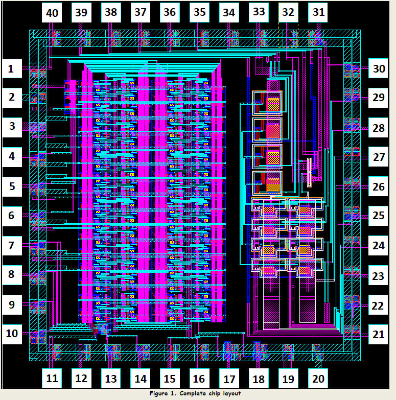
The chips purpose along with the PCB is meant to test for photon
counting as there are two parts to the chip. A 64 stage wide-swing fast
transient digitizer and a 4-channel sample and hold array, where for
this research work the sample and hold array is what is being tested.
Click this link here for more info on the layout (seen below) and organization of the chip.
4-Channel Sample and Hold PCB
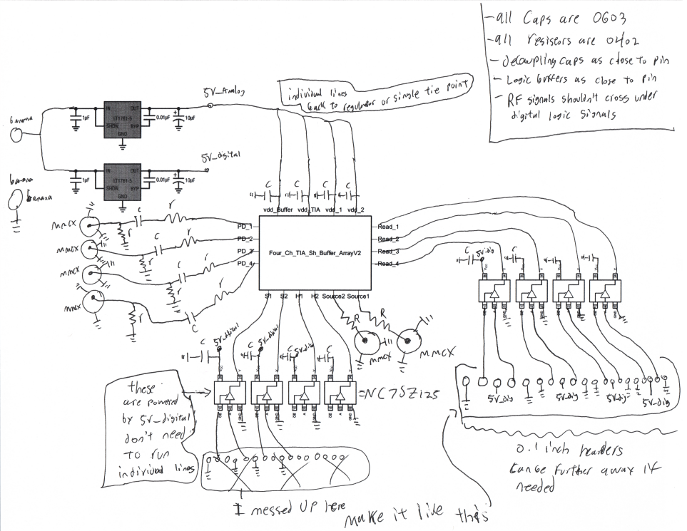
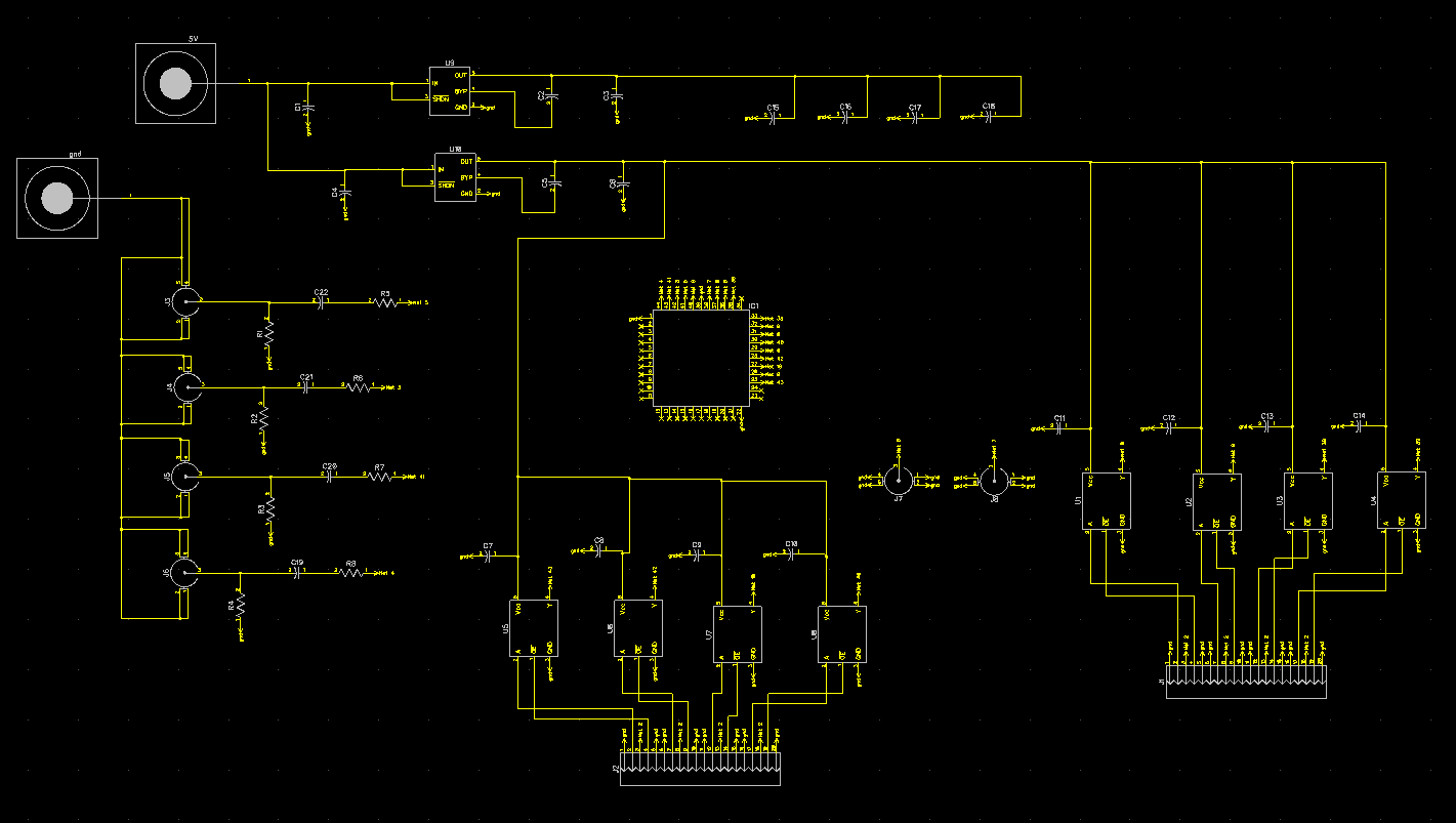
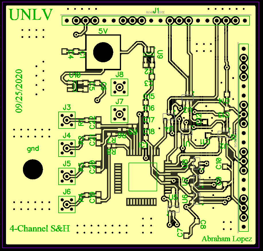
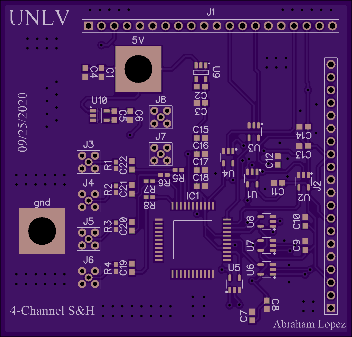
A draft of a schematic designed by Angsuman Roy
was given to me to design in DipTrace. The schematic is comprised of
the chip supported by on-board components such as 5V regulators to
power the chip and logic buffers. MMCX connectors to send machine code
to the chip and male pin headers connected to different outputs and
inputs in order to verify the operation of the chip using an
oscilloscope. The schematic, PCB layout and more can be seen below.
Draft of schematic
Schematic in DipTrace
PCB Layout
Rendering from Oshpark
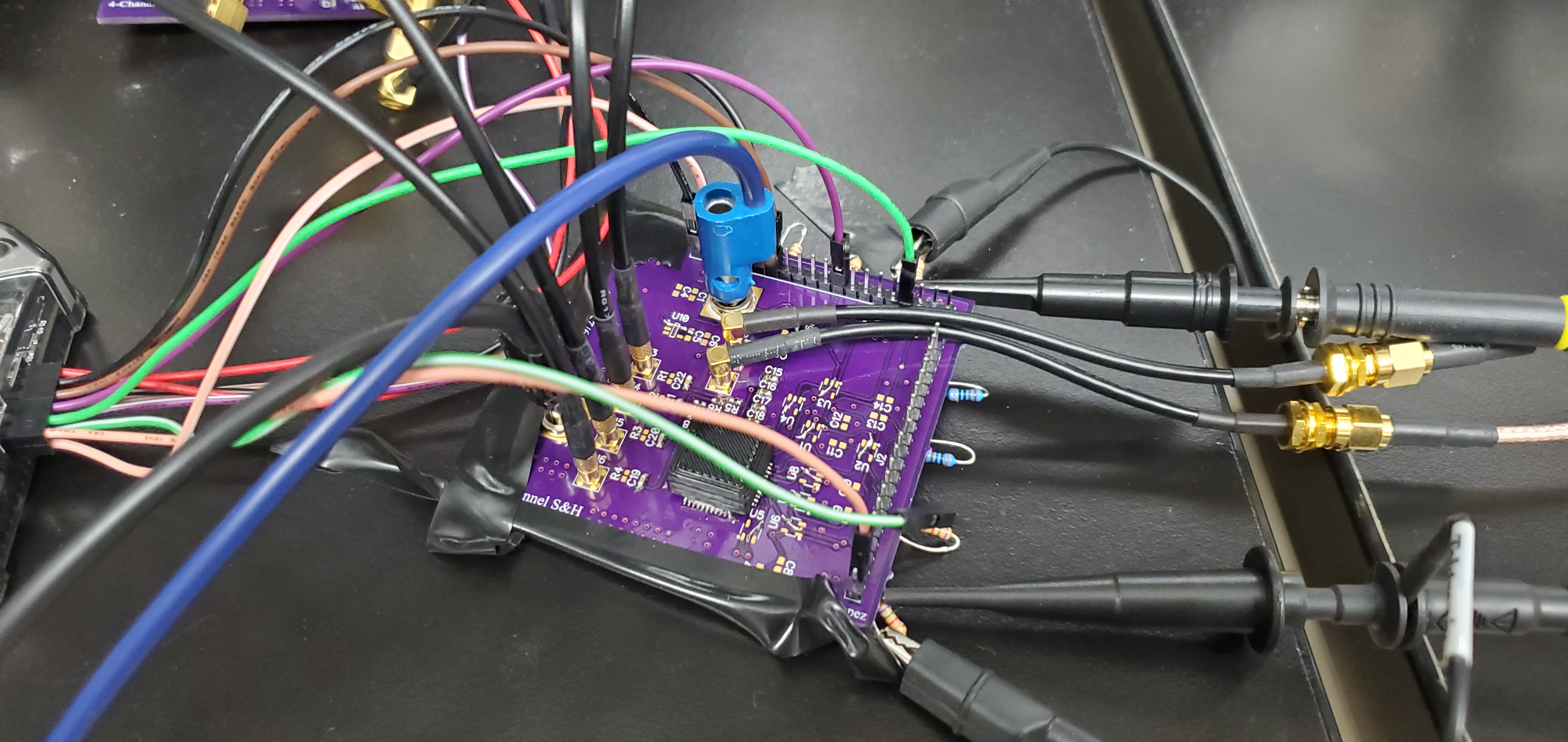
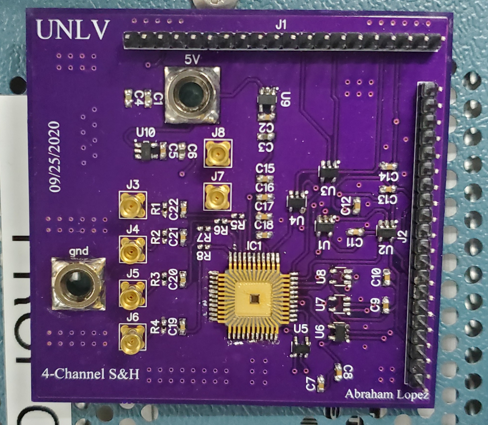
Fully Populated S&H PCB
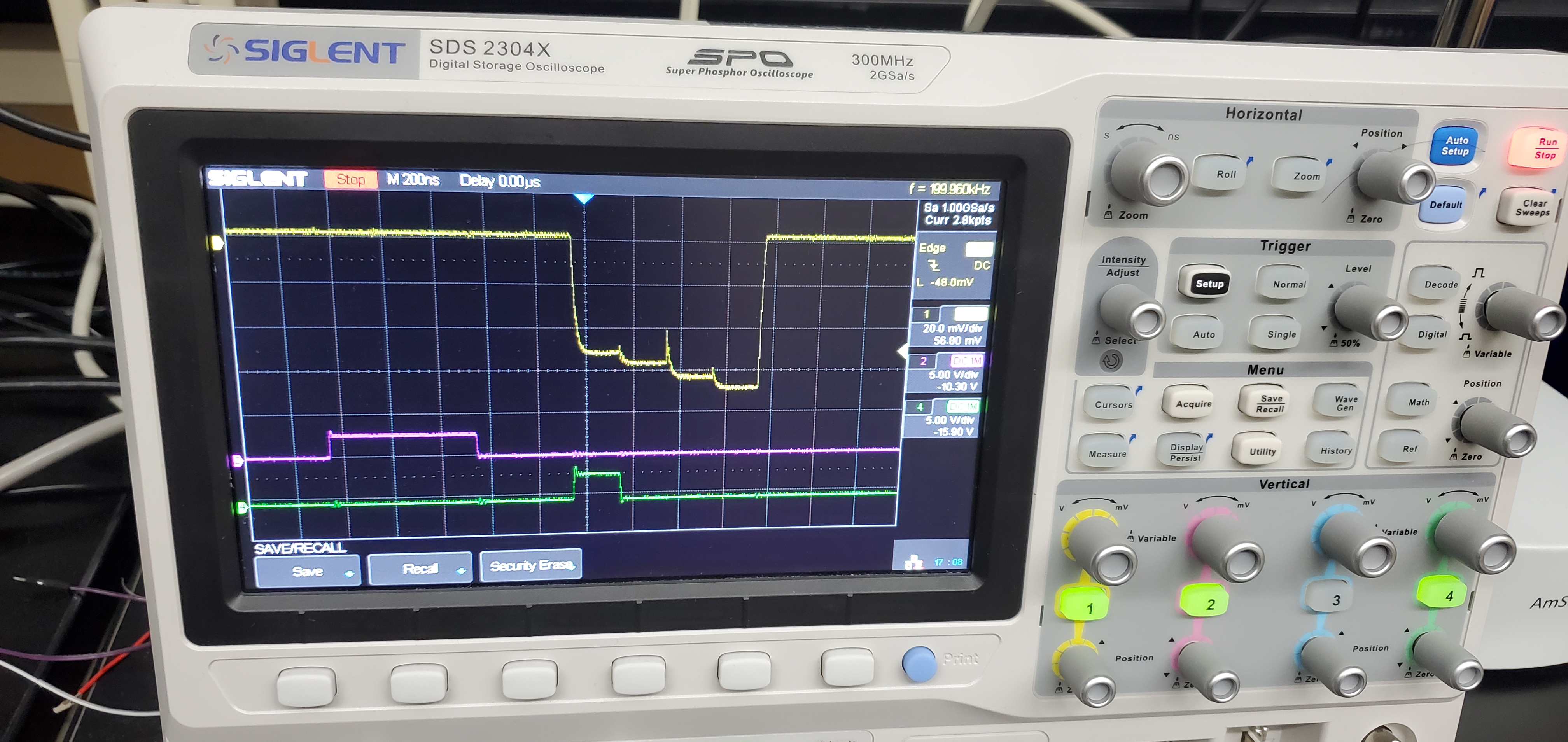
Setup & Testing of PCB and Chip