Final Project - EE 421L
Authored
by Batya Vishnepolsky, vishnepo@unlv.nevada.edu
Final Project Description:
Design a non-inverting buffer circuit that presents less than 100 fF
input capacitance to on-chip logic and that can drive up to a 10 pF
load with output voltages greater than 7V (an output logic 0 is near
ground and an output logic 1 is greater than 7V). Assume VDD is between
4.5V and 5.5V, a valid input logic 0 is 1V or less, a valid input logic
1 is 3V or more. Show that your design works with varying load
capacitance from 0 to 1pF. Assume the slowest transition time allowed
is 4 ns.
Design Process
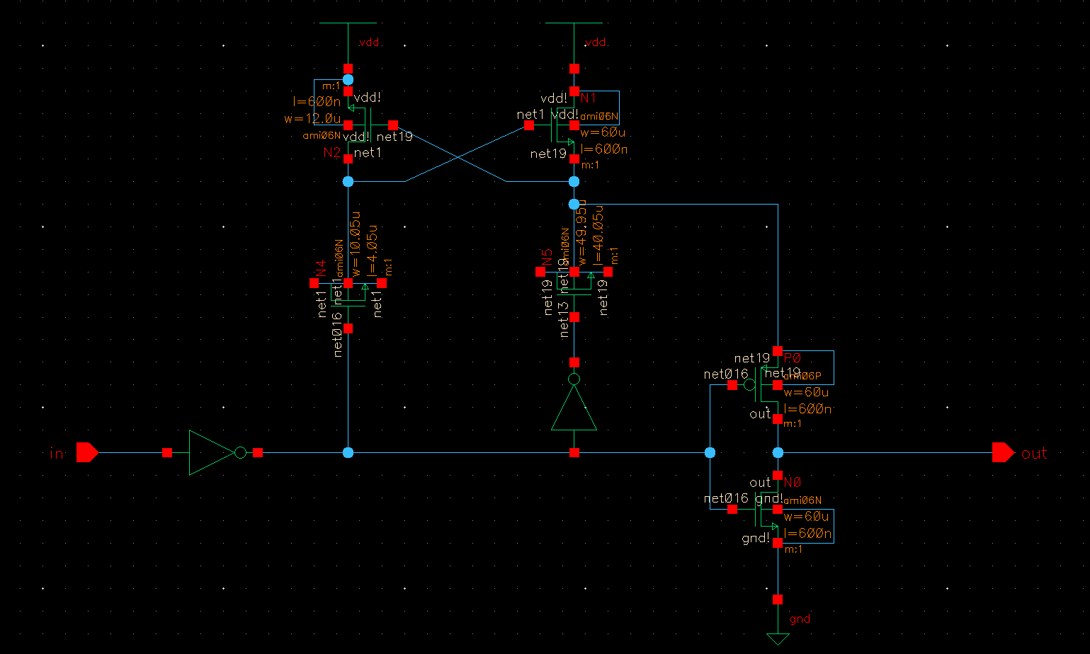
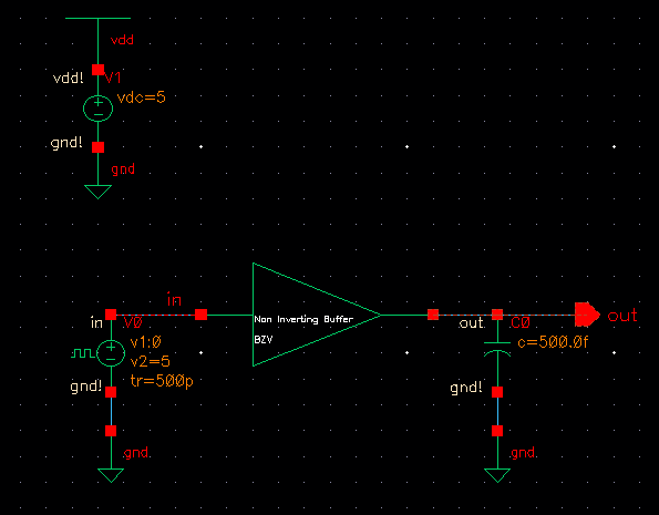
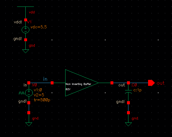
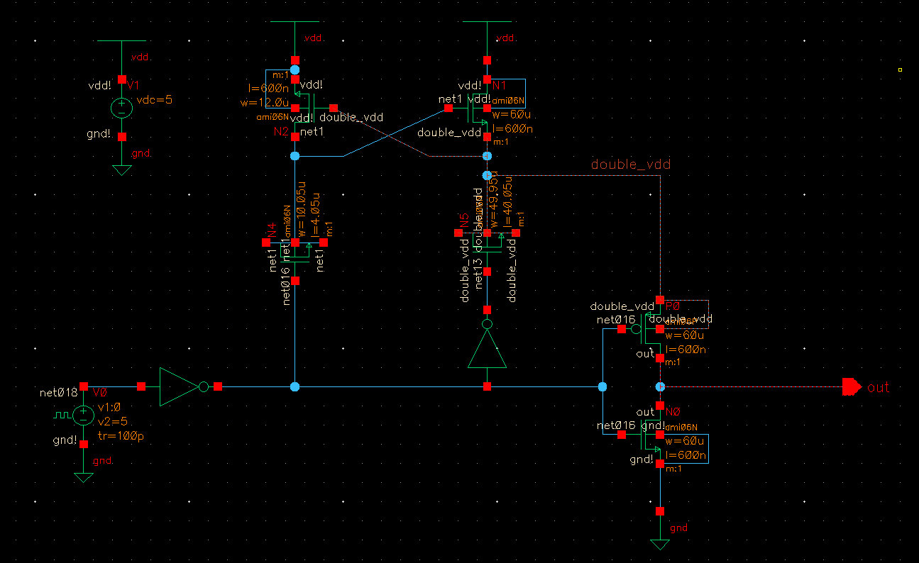
After learning about a lot of circuit/ buffer topology from chapter 18 of our textbook, I designed the following circuit:
Circuit:
Design decisions included:
- Determining sizing of mosfets
- The MOSFET N2 is smaller than the N1 because this will save
layout space as well as not waste power. N2 and N4 both don't supply
any power to the output of the circuit. The primary purpose of this
NMOS is to turn on N1 and precharge the output node to VDD.
- I
chose to do a 60/.6u size for the inverter on the end of the circuit
(P0 and N0) as well as N1 (the NMOS on the top left) because it would
drive a higher current. Why? Because as one increases the width of the
current, the effective resistance of the MOSFET gets lower (V=IR, ohms
law).
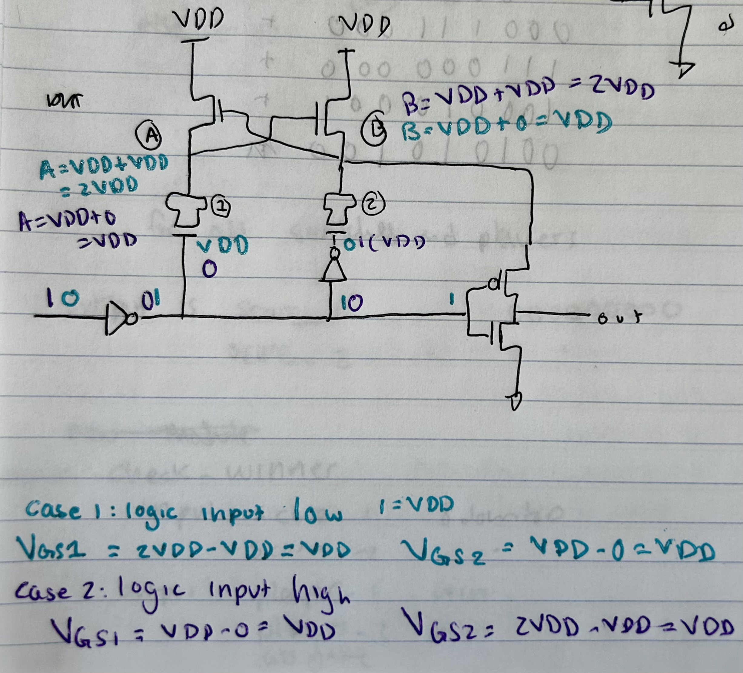
- Creating mosfets in place of capacitors
- The operation of the MOSFETS is always in strong inversion, which means the two mosfets N3 and N4 will behave as capacitors
Explanation:
What happens to an NMOS in strong inversion? A large amount of
electrons are attracted to under the gate, and the capacitance will
increase at the gate the greater Vgs is then Vth. The electrons that
are attracted to the gate will short the drain and the source together.
This forms a low resistance "bottom plate" for the capacitor.
How do we know our MOSFET is always in strong inversion? In order for a mosfet to be
in strong inversion, the Vgs (Voltage difference from the gate to the
source) must be a lot bigger then the Vth (threshold voltage). For the
case of an NMOS in the C5 process,
the threshold voltage is 0.7V. And the Vgs will always have a Vdd difference. Why? Take a look at these hand calculations:
Essentially, no matter the input of the circuit, the difference across
the MOSFETs will always be VDD. VDD is at minimum 4.5V (due to
constraints of the project), and 4.5V - 0.7V = 3.8V. 3.8V is
more then 5 times larger than the Vth, and therefore the MOSFETS are in
strong inversion, and behave as capacitors for the circuits operation.
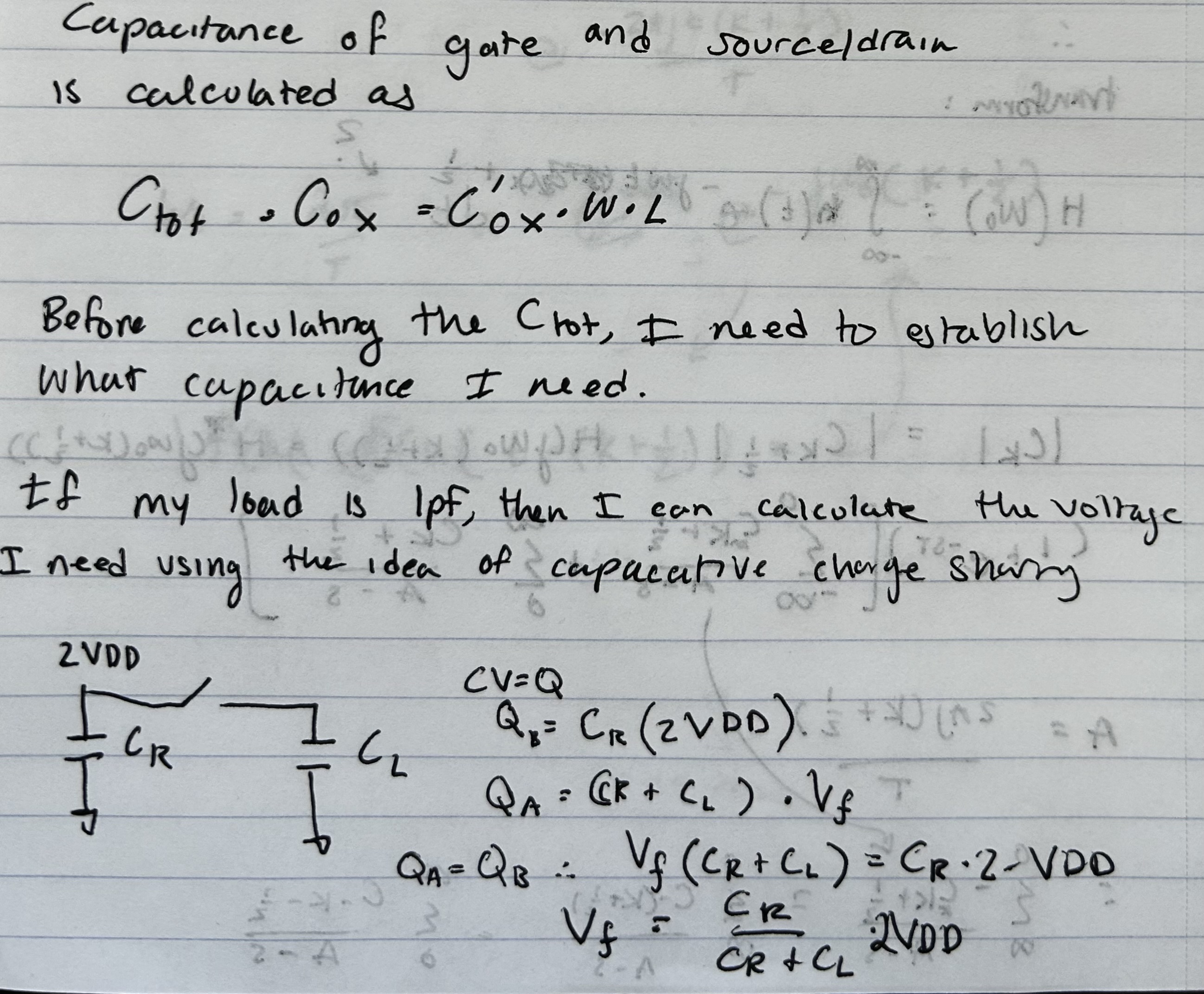
- The equivilant capacitance (dependant on the load).
Explanation:
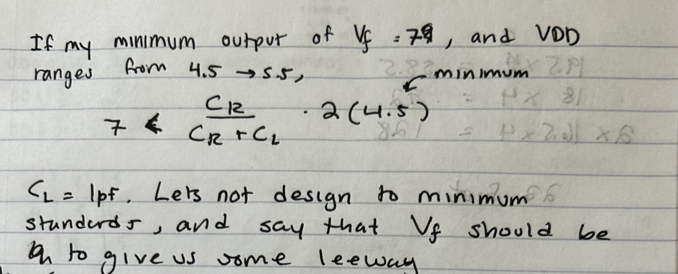
In order to ensure that the output voltage will remain above 7V for the
entirety of operation, we need to size the MOSFETs correctly, as the
length and width of the MOSFET have a direct relationship with it's
equivalent capacitance.
For the MOSFET N5, it was sized as such:
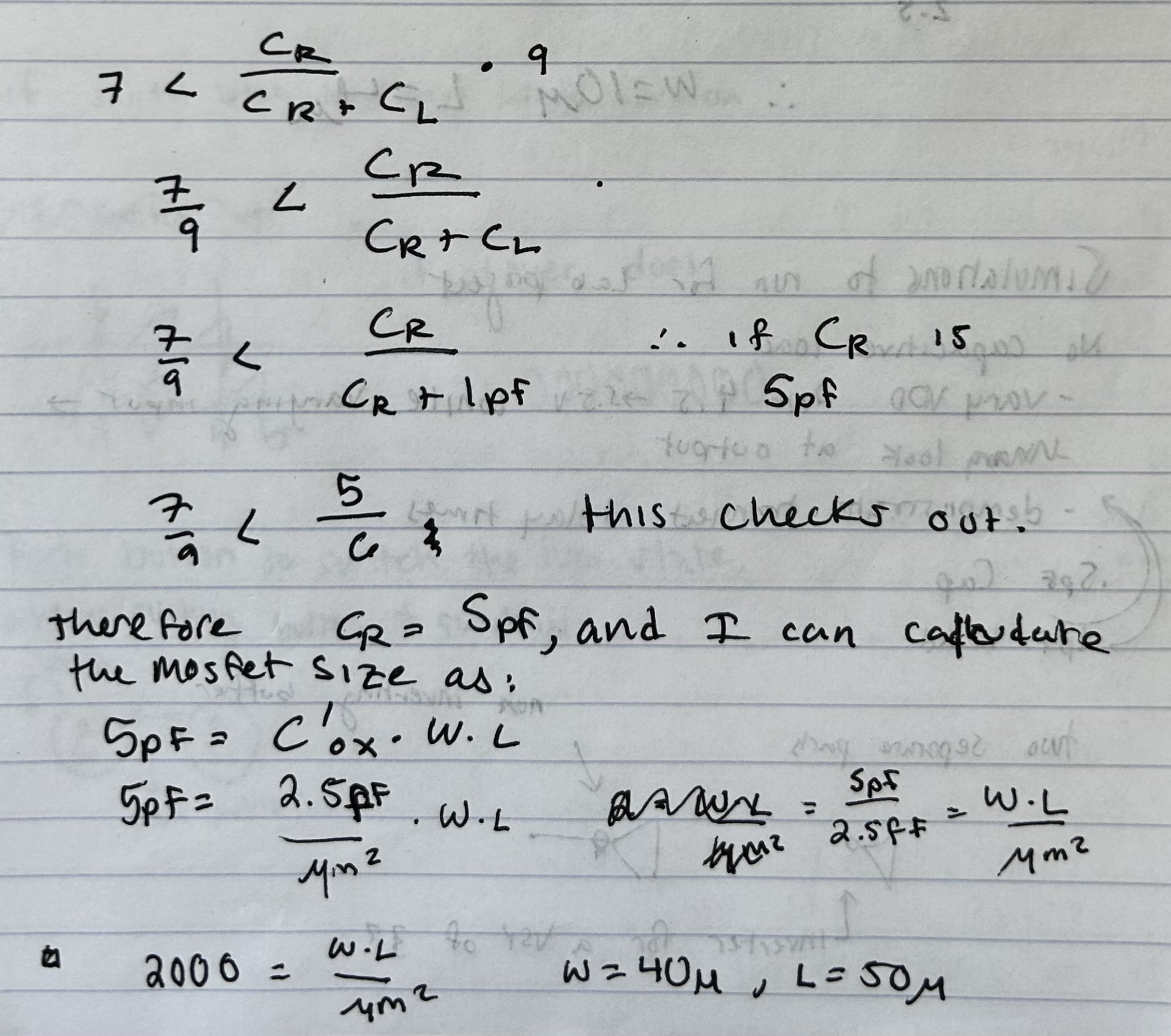
The other capacitor, N4, can be smaller because it is not going to affect the output voltage.
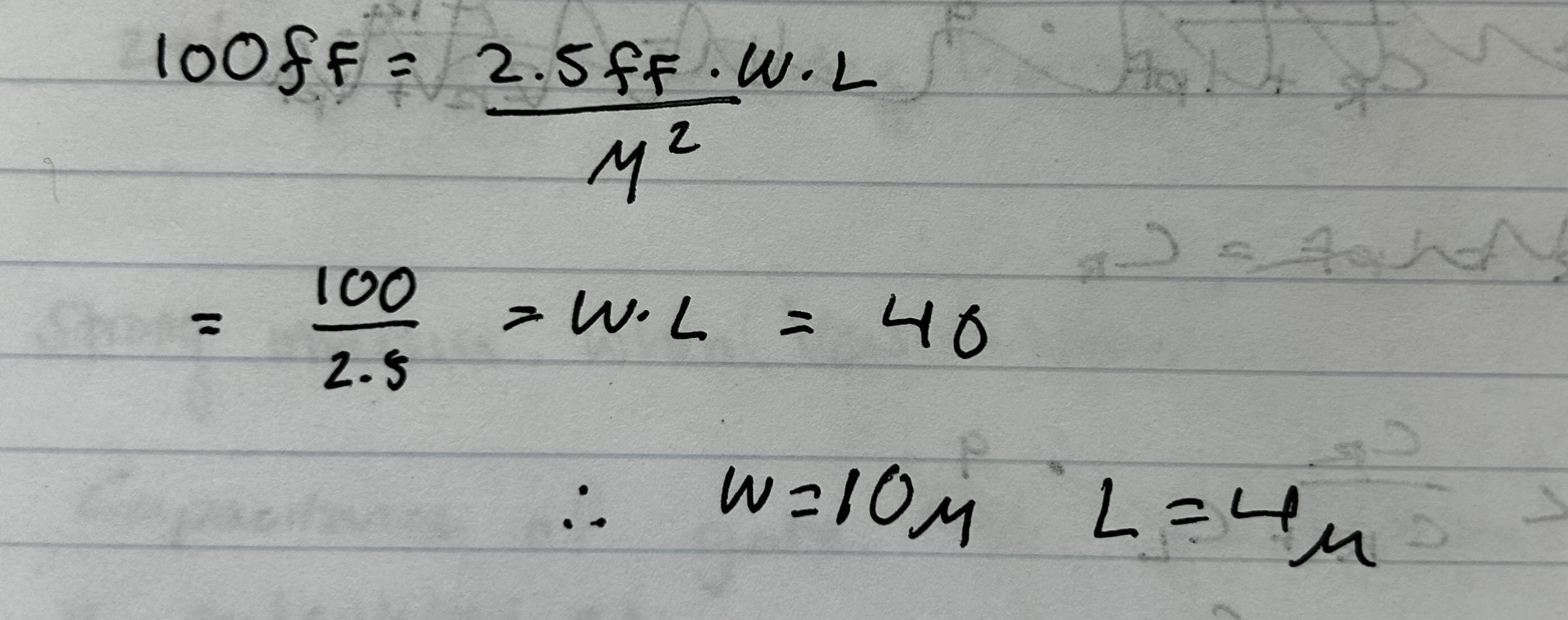
For the MOSFET N4, it was sized as such:
I decided to size N4 to have an equivilant capacitance of 100fF:
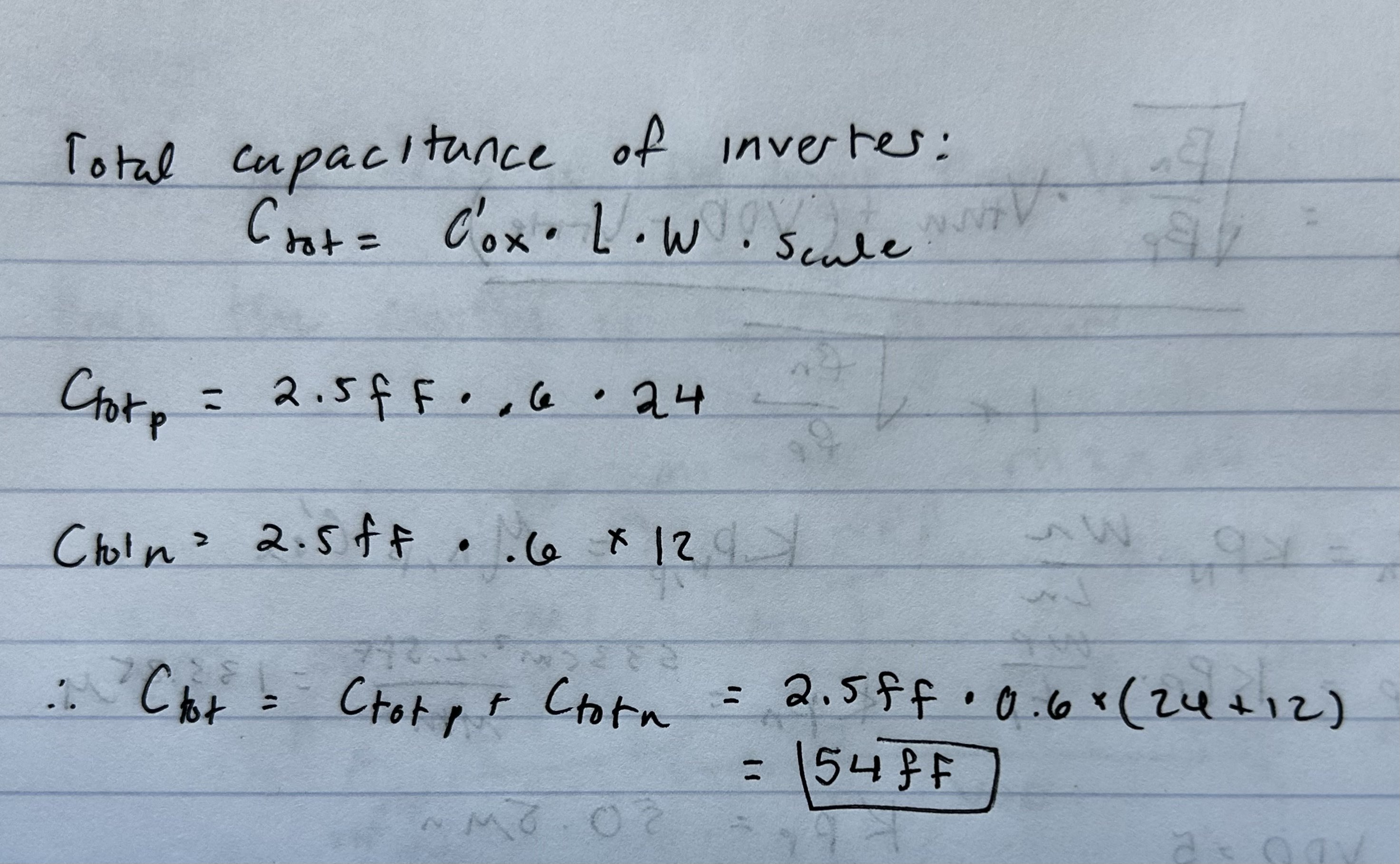
- Inverter switching point (Seen below on the explanation for the inverter's internal view).
Internal view of the inverters on the schematic:
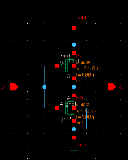
I chose to do an inverter
where the PMOS was double the size of an NMOS, because the switching
point of this inverter is about 2.5 when VDD is 5. I have done this in
previous class assignments.
However, one can also calculate the switching point (VSP) of the inverter by using the following equation:
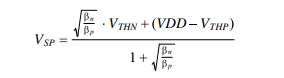
Something else to consider, is that the ratio of ßn/ßp
affects the voltage's switching point. When you increase the strength
of the NMOS, the switching voltage decreases, and when you increase the
strength of the PMOS, it will increase. If we needed to alter the Vsp
for different values, we could either mathematically calculate it using
the above equation or "guess and check" by increasing/ decreasing the
sizes of our NMOS or PMOS, depending on the Vsp needed.
How would one increase the
strength of the ßn,p? The relationship between the ß variable and the
size of the transistor is as such: ßn,p = Wn,p/Ln,p. Seeing this, it is clear that one would need to increase the width of the transistor.
Additionally, the input capacitance must be less then 100fF, which it is, as seen through this math:
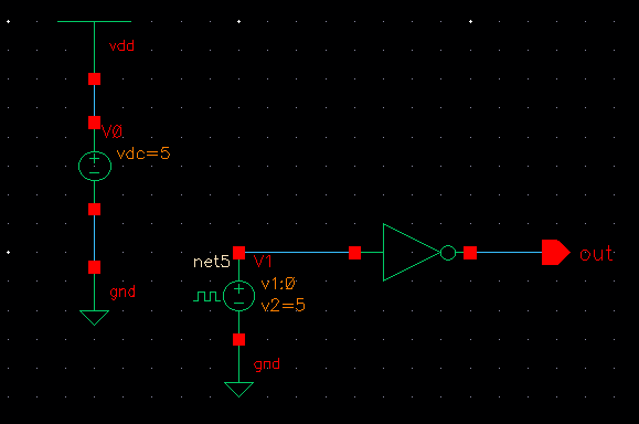
Simulations to demonstrate switching point as VDD varies from 4.5 - 5.5:
Setup:
Simulation at 4.5, 5, and 5.5 switching points:
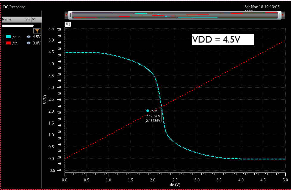
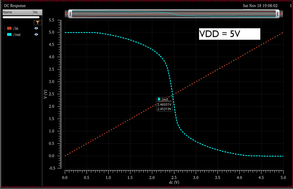
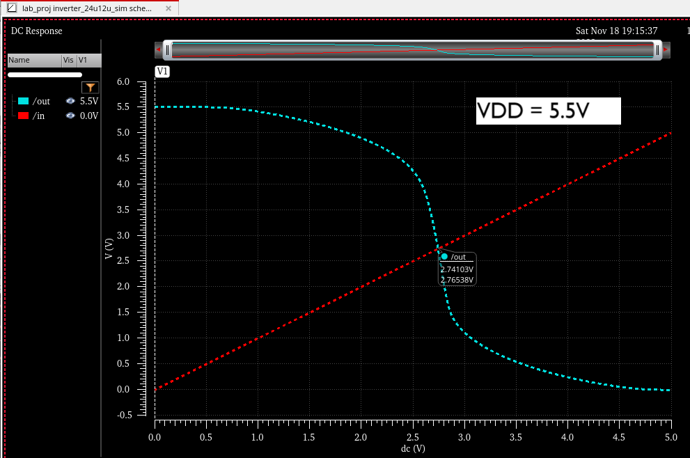
As you can see, the lowest switching point is 2.19V and the highest switching point is 2.74V.
This falls in the paramaters of the project specifications, which
indicate a logic low of 1V or less, and a logic high of 3V or more. The
swtiching point remains in between 1 and 3 during every VDD.
After verifying correct
inverter operation, and creating the entire charge pump schematic, I created a symbol view
of the non inverting buffer and labeled if accordingly:
Symbol:
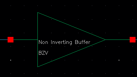
I then created a seperate cell view to simulate the operation of my non inverting buffer to ensure that it acted as expected.
Simulations:
I simulated my design using no capacitave load, a .5pF load, and a 1pF
load.
Within each capacitive load simulation, I did a transient
simulation to demonstrate the rise and fall times and DC simulation to
simulate the following:
- The affect on the output voltage with a varying VDD
- The effective delaly of the rise and fall times with different
loads. You don't need to vary the VDD in this simulation because the
rise and fall times are independant of the VDD. They are a calculations
of resistance and capacitance.
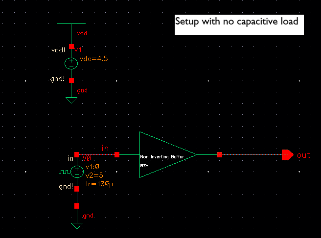
Simulation setup (with no capactive load):
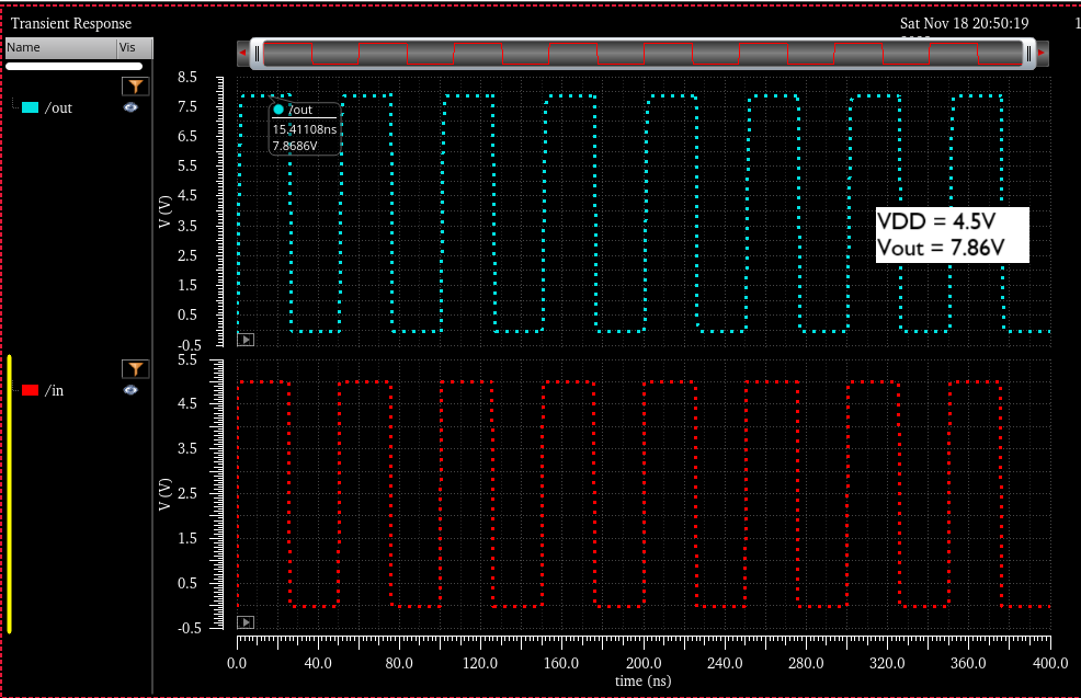
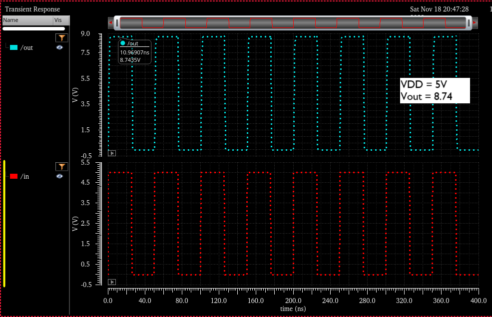
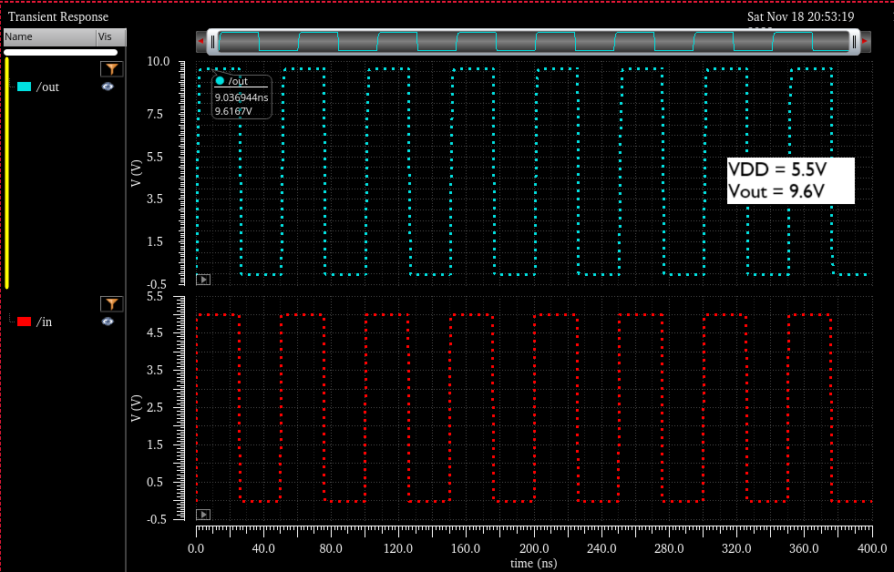
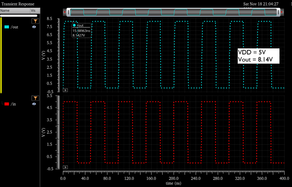
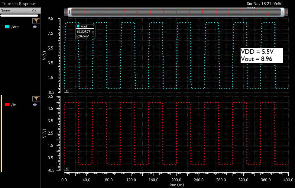
Vout with a varying VDD:
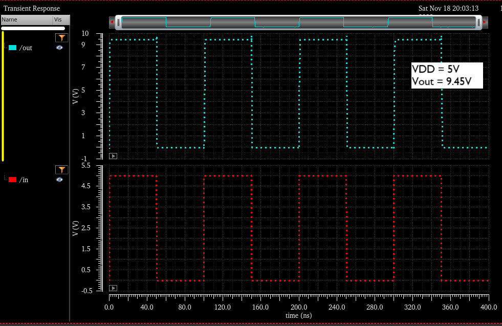
As you can see, Vout remains above 7V regardless of VDD when there is no capacitave load present.
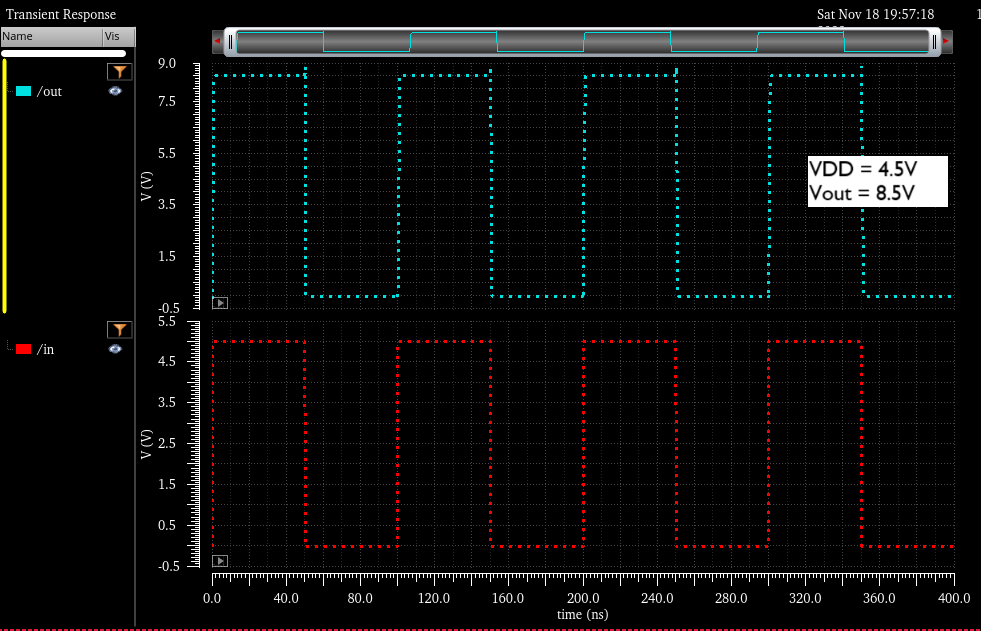
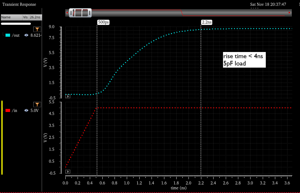
Delay times with no load:
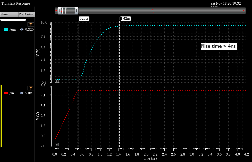
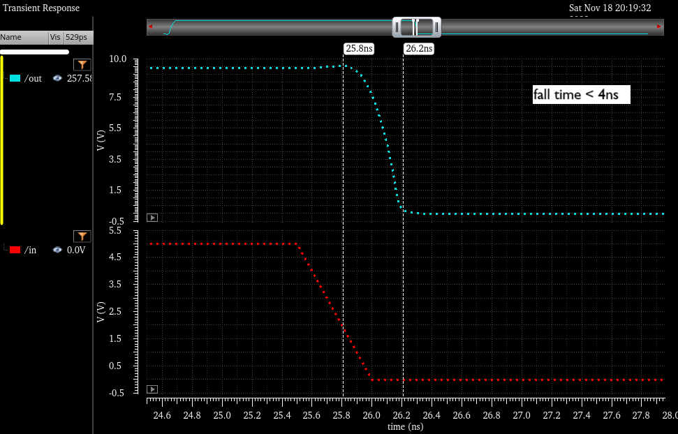
With an input rise time and
fall of 500pF, the rise and delay times of the output are still under
4ns, which complies with the design parameters.
Simulation setup (with .5pF load)
Vout with a varying VDD:
Once again, the voltages remain above seven for the output.
Delay times with .5pF load:
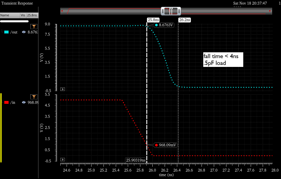
And here we also see that the delays are under 4ns.
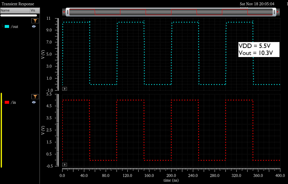
Simulation setup (with 1pF load)
Vout with a varying VDD:
Once again, the voltage remains above 7V for the entirety of the simulation.
Delay times with 1pF load:
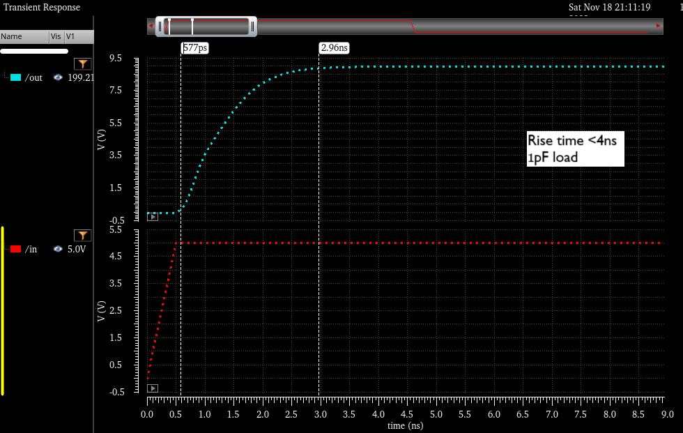
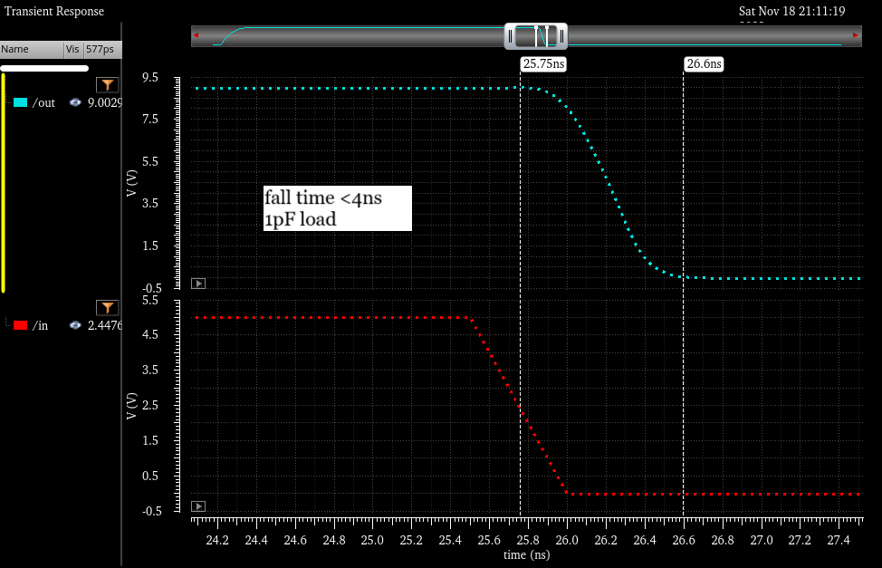
And here we can also see that the delay for the rise and fall are also less then 4n.
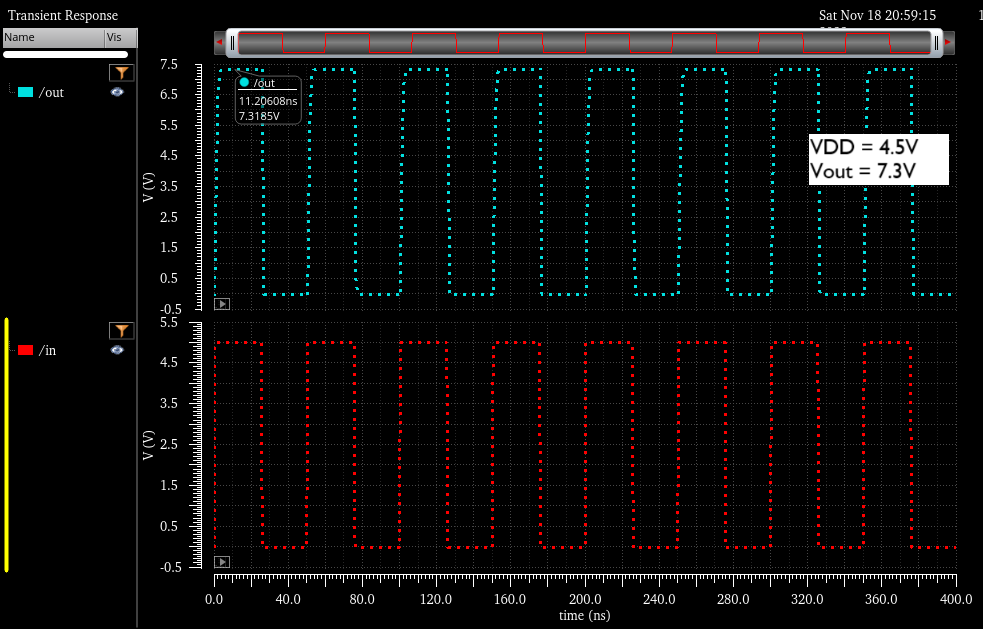
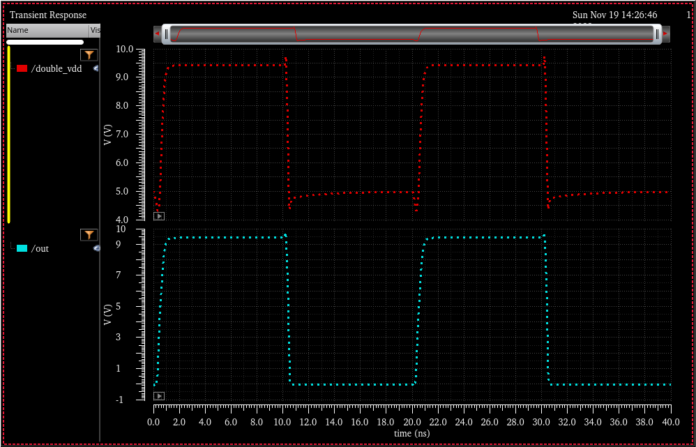
One last simulation I want to demonstrate is how the output voltage will get the total of 2VDD:
I created a simulation to simulate the node right before the output,
and labeled it "double_VDD". As you can see from the simulation, it
oscillates from VDD to 2VDD. The reason is that its "baseline" charge
is VDD from the NMOS above it, and when the logic input of the entire
schematic is high, it becomes VDD + VDD = 2VDD, as demonstrated in the
simulation.
And that concludes the part of the lab for the simulations and math behind my design.
After showing the schematic and simulations to Dr. Baker for the first
half of my project, I was corrected in my orientation of MOSFETS N1 and
N2. The orientation gives the MOSFETS a negative Vgs instead of a
positive Vgs, which means that the MOSFETS are not operating in strong
inversion, but they are actually operating in accumiliation instead of
strong inversion. The MOSFETS were still working, but with an
additional resistance. This is why my output was a little less then
double Vdd. I did not catch this right away because I designed past
minimum standards and the project was still working for what was
needed. I kept the orientation as such to save time.
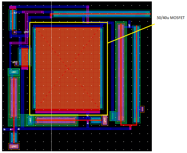
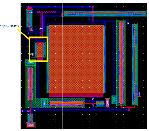
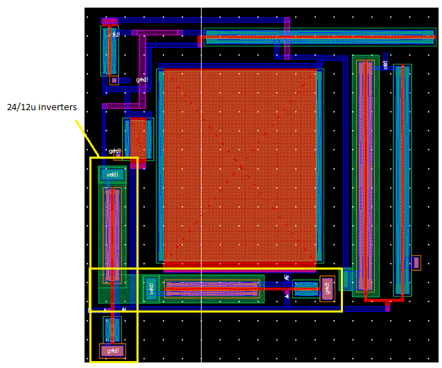
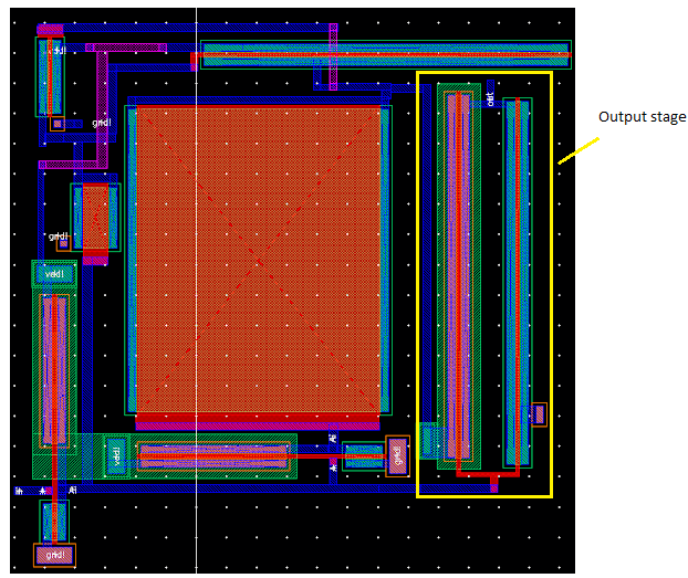
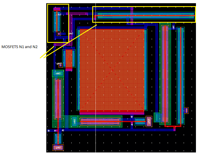
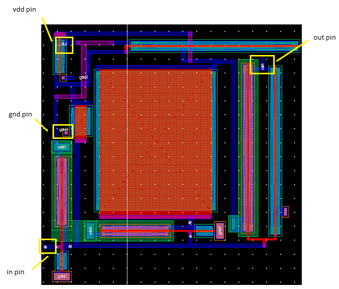
The next part of my project was creating the chip fabrication layout for the circuit. And this is what it looks like:
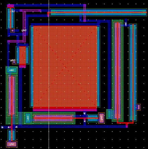
The biggest part of the chip, the MOSFET in the middle is this
component sqaured in red. This is the 50/40u mosfet that creates the
5pF capacitance. If you look at the left and right blue lines, that is
our source and drain, they are shorted together and are wired to other
components in the circuit.
This is the smaller capaciter sized at 100fF. The drain and source are also shorted together over here.
These components are the 24/12u inverters that are present in our
circuit. They share the same N-well, as you can see the green
connection.
This is the output stage that is also an inverter. It is in it's own
well, and to save space on the layout I "folded" it in half. It is
connected with the m1 layer to the drain to the upper right NMOS and
the output.
These are the upper mosfets, N1 and N2. Notice how the top left is
smaller sized. This again is to optimize power loss because the left
mosfet is not needed to drive a higher voltage.
These are the pins on my schematic: in, out, gnd!, vdd!. The ! means that the pin is referencing a global variable.
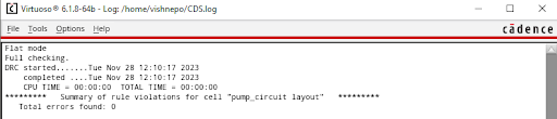
To verify my layout is follows design rules and can be fabricated, I
run a DRC (design rules check) and verify my layout's accuracy.
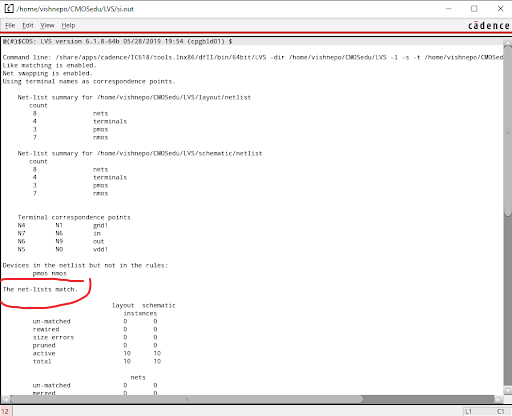
I extracted the layout, and run a LVS to ensure that my layout matches my schematic and isn't something different.
I also backed up all my files, and have included a zip below if anyone wishes to run the project on their own machine.
Lab_Proj.zip
That concludes my project!
Return to all of Batya's Labs