Lab 4 - ECE 421L
IV Characteristics and Layout of NMOS and PMOS DEVICES
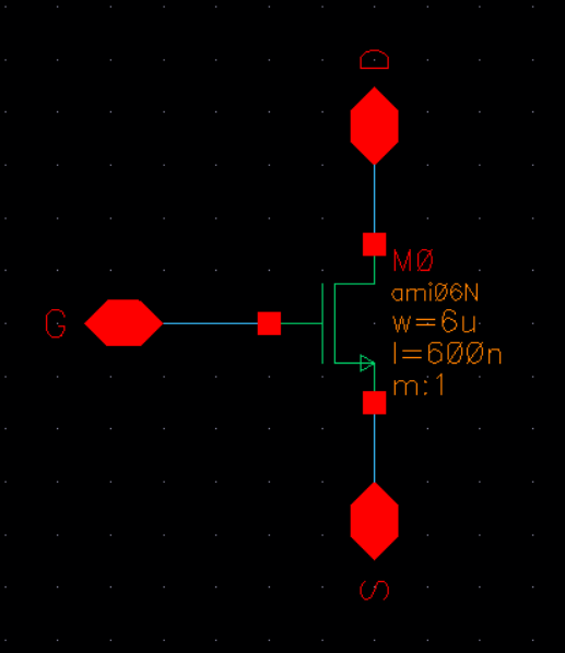
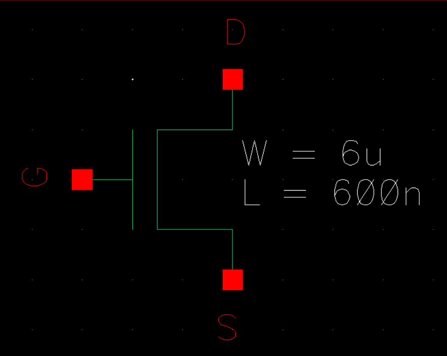
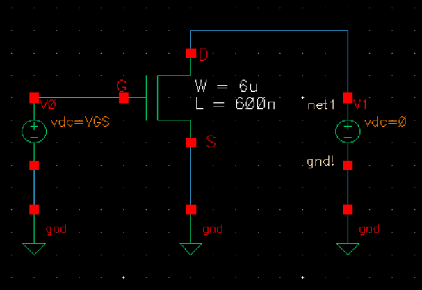
Following the instructions of Tutorial 2, we create a schematic then a symbol for an NMOS.
After which, we created a circuit with the symbol we created.
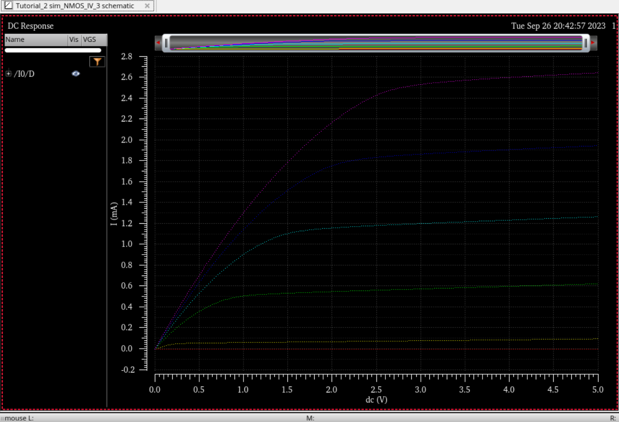
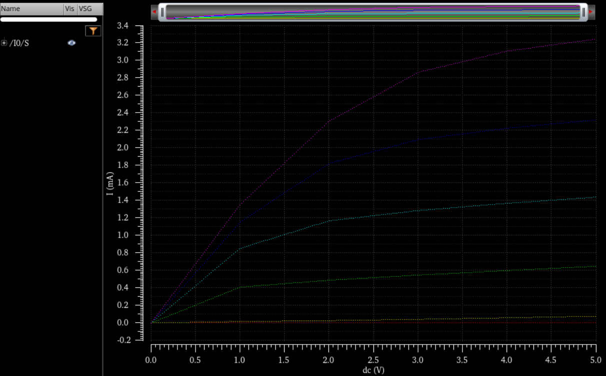
Then we ran a parametric anaysis on the circuit.
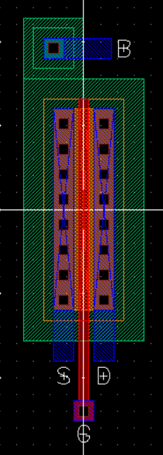
From the schematic, we created a layout for the NMOS.
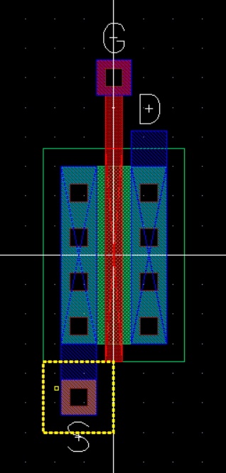
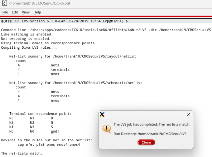
We then extract the layout then performed an LVS to make sure the netlist matches.
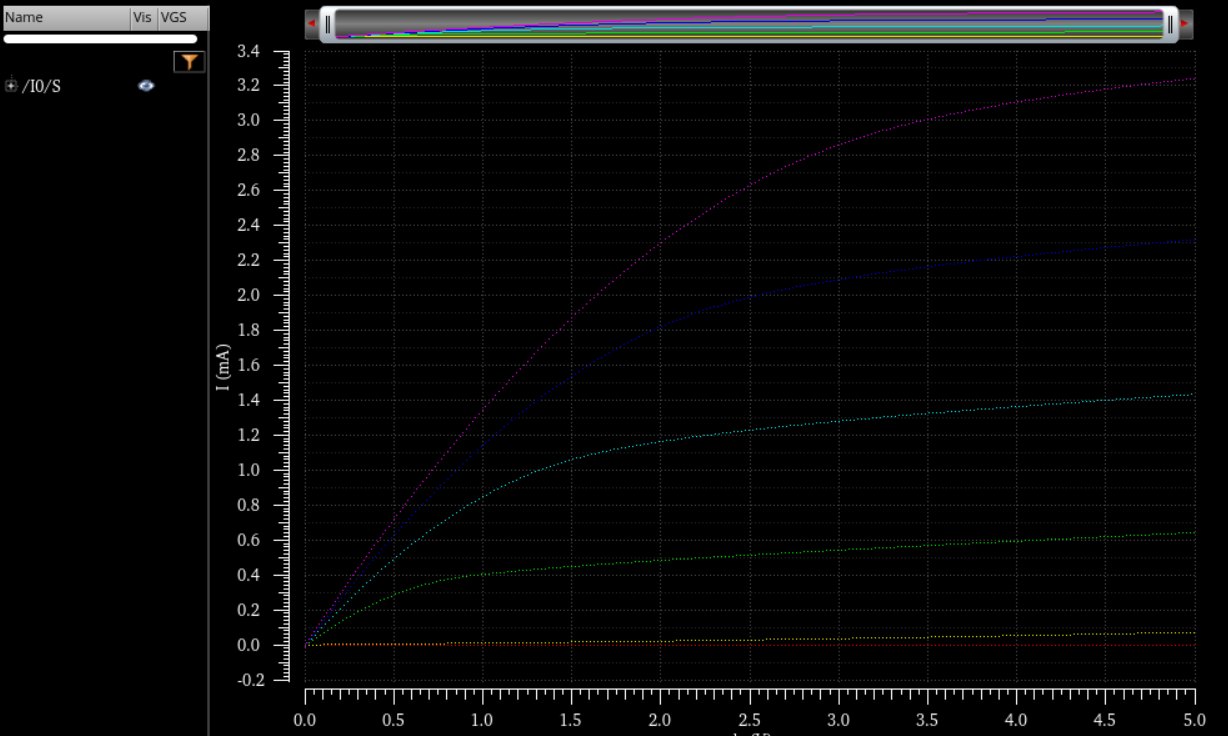
We then run a final parametric anaysis.
Now we want to repeat the previous steps for a PMOS. We tart by creating a schematic and symbol.
After which, we created a circuit with the symbol we created.
Then we ran a parametric anaysis on the circuit.
From the schematic, we created a layout for the PMOS.
We then extract the layout then performed an LVS to make sure the netlist matches.

We then run a final parametric anaysis.
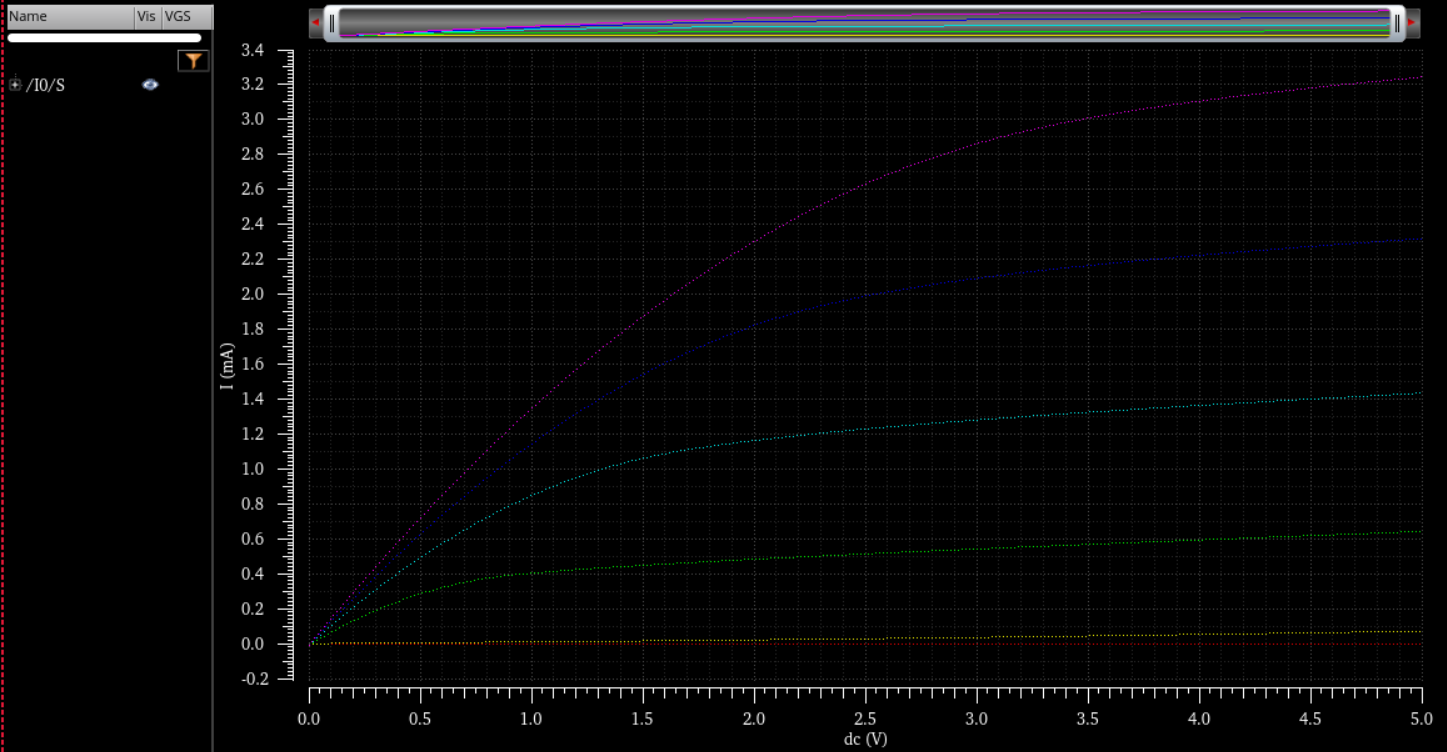
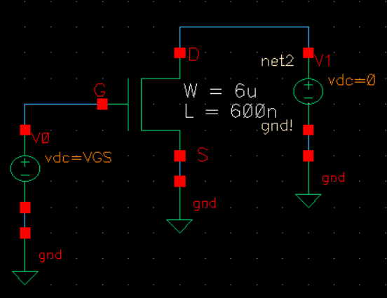
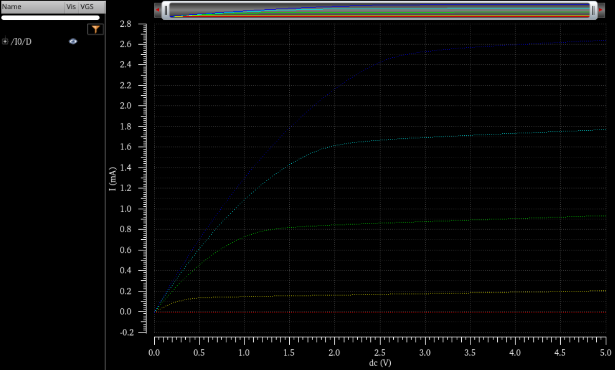
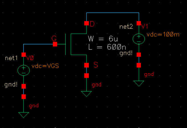
First, we created a schematic for simulating ID v. VDS of an NMOS device for VGS varying from 0 to 5 V in 1 V steps while VDS varies from 0 to 5 V in 1 mV steps. We use a 6u/600n width-to-length ratio then generated a parametric analysis.
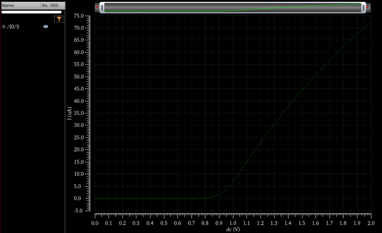
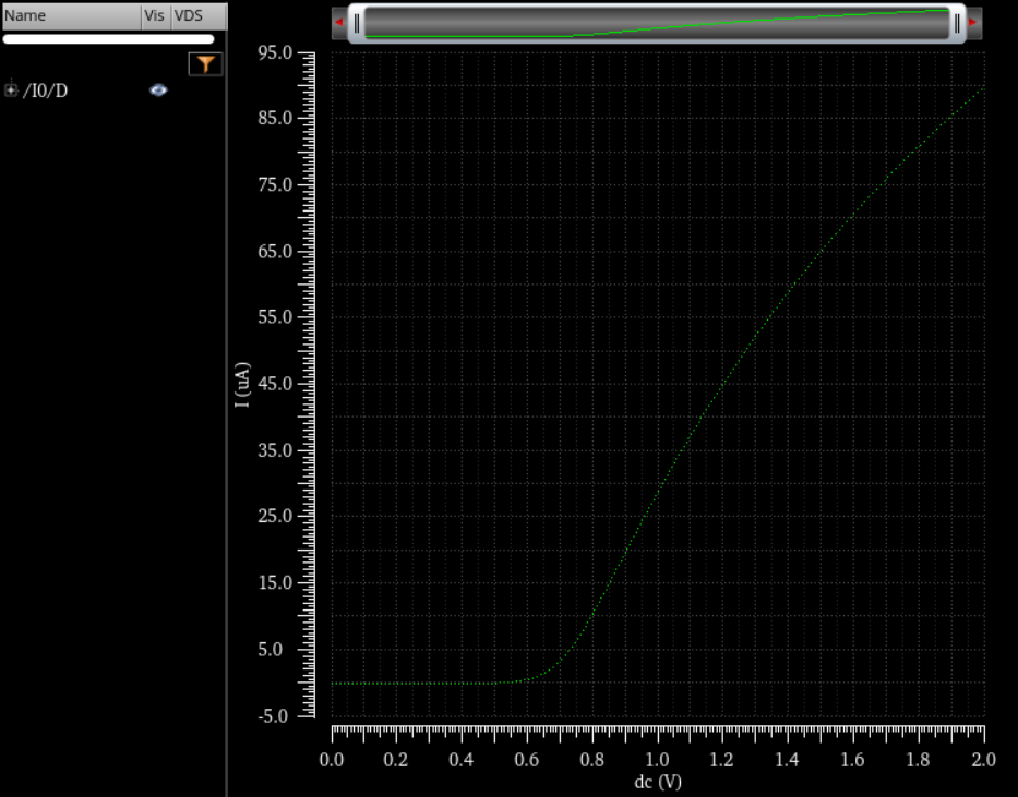
Second, we made a schematic for simulating ID v. VGS of an NMOS device for VDS = 100 mV where VGS varies from 0 to 2 V in 1 mV steps. Again use a 6u/600n width-to-length ratio was used and we generated a simulation.
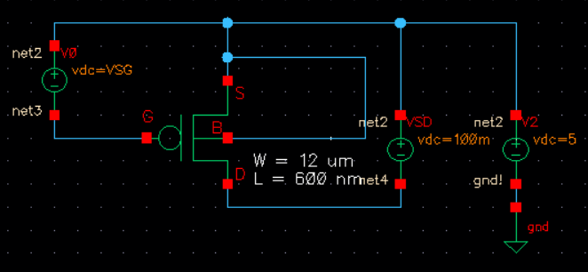
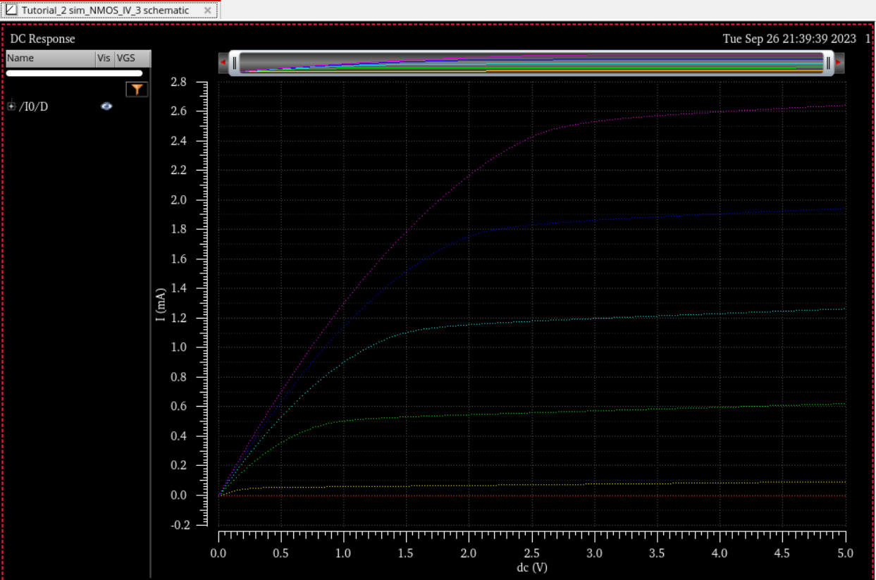
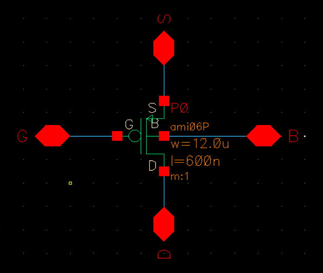
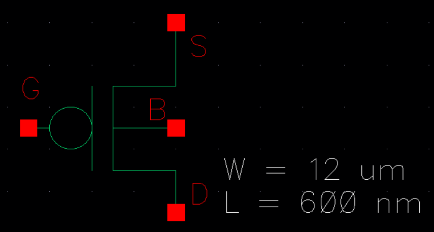
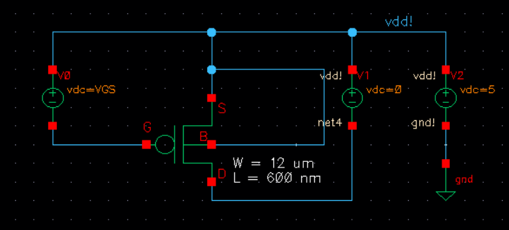
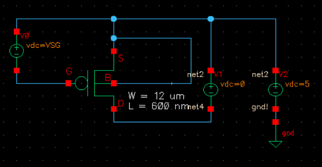
Third, we make schematic for simulating ID v. VSD (note VSD not VDS) of a PMOS device for VSG (not VGS) varying from 0 to 5 V in 1 V steps while VSD varies from 0 to 5 V in 1 mV steps. We used a 12u/600n width-to-length ratio and ran a simulation.
Lastly, we created another schematic for simulating ID v. VSG of a PMOS device for VSD = 100 mV where VSG varies from 0 to 2 V in 1 mV steps, then ran another simulation.