Lab 3 - ECE 421L
Layout of a 10-bit digital-to-analog converter (DAC)
This pre-lab continues to work through Tutorial 1
which was started in lab 1. Please see lab 1 for preceeding
steps. We begin this pre-lab by creating a schematic for a 10k
ohm voltage divider.
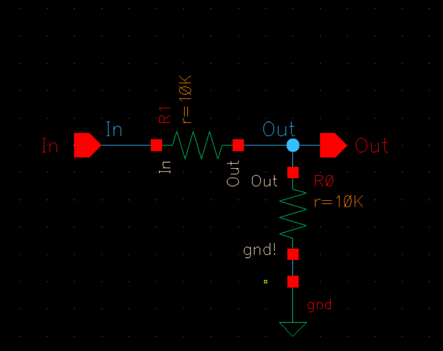
From the completed schmatic, we can then convert it into symbol format where I used the create shape feature to draw out the resistors and ground.
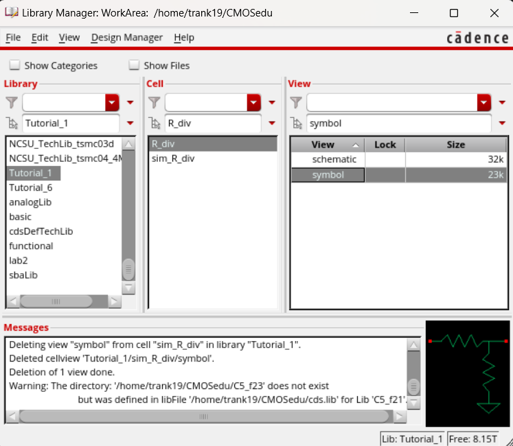
I then create a copy of the R_div cell in the Library Manager and name it sim_R_div, where I will further develope the circuit.
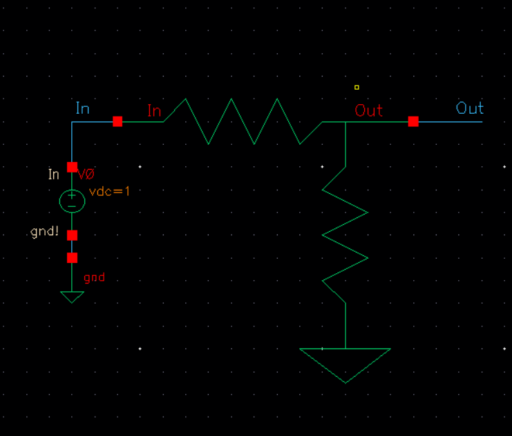
With the symbol previously created, I impement it into a circuit by adding a voltage source.
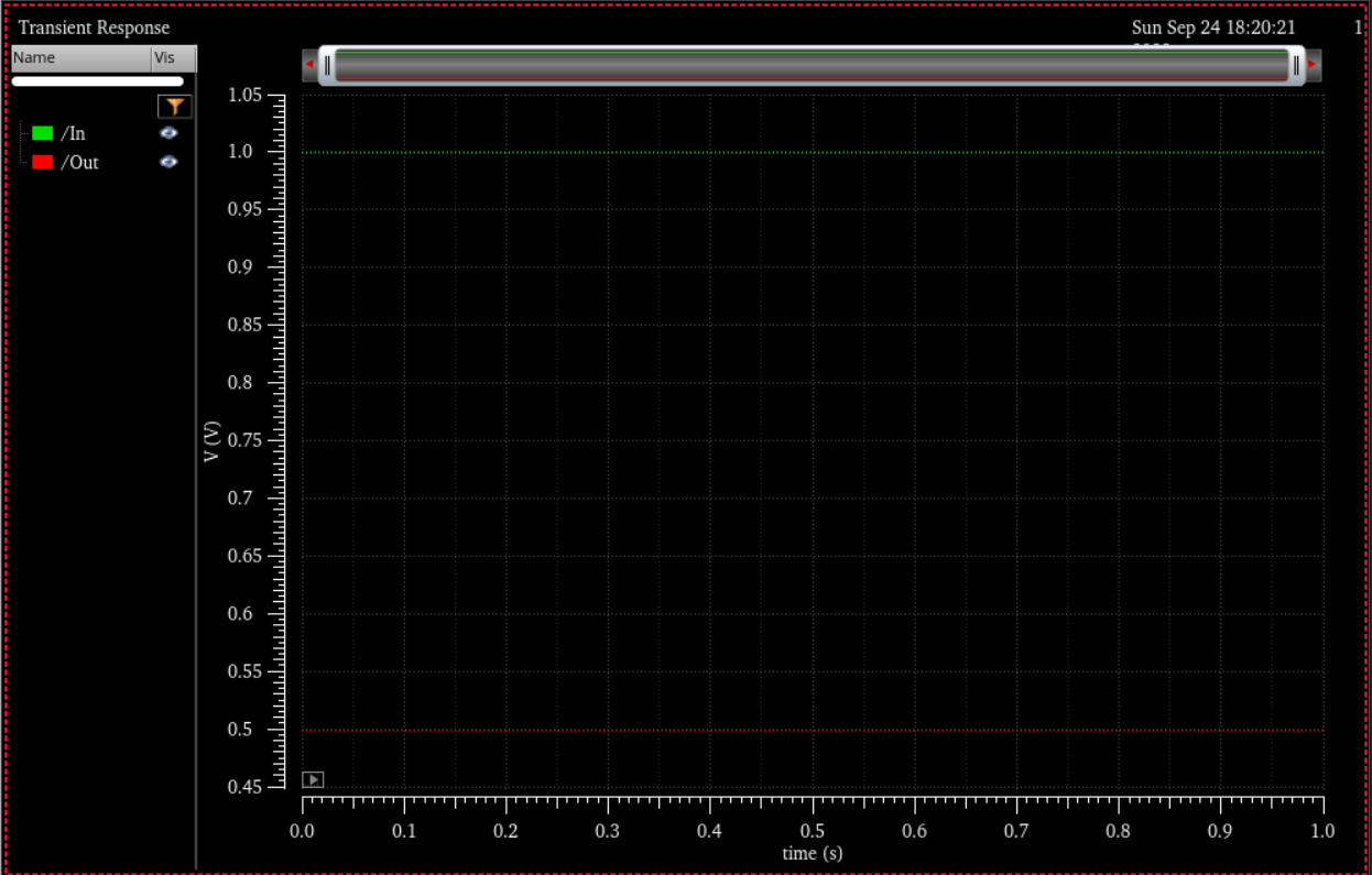
We then run a simulation of the circuit and confirm the behavior that is expected.
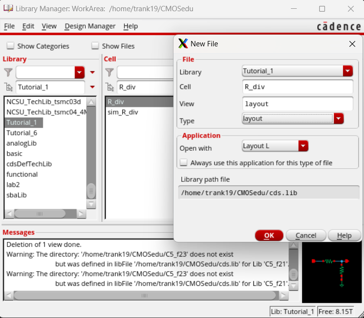
With the schematic functioning as intended, we then move on to creating the layout in the Library Manager.
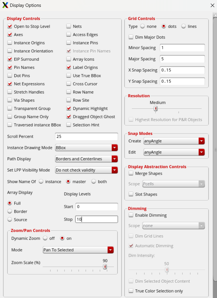
Using the keyboard shortcut "E", the display options menu is opened and we want to allow pin names and a maximum of 10 layers shown. The snap modes are also set to anyAngle.
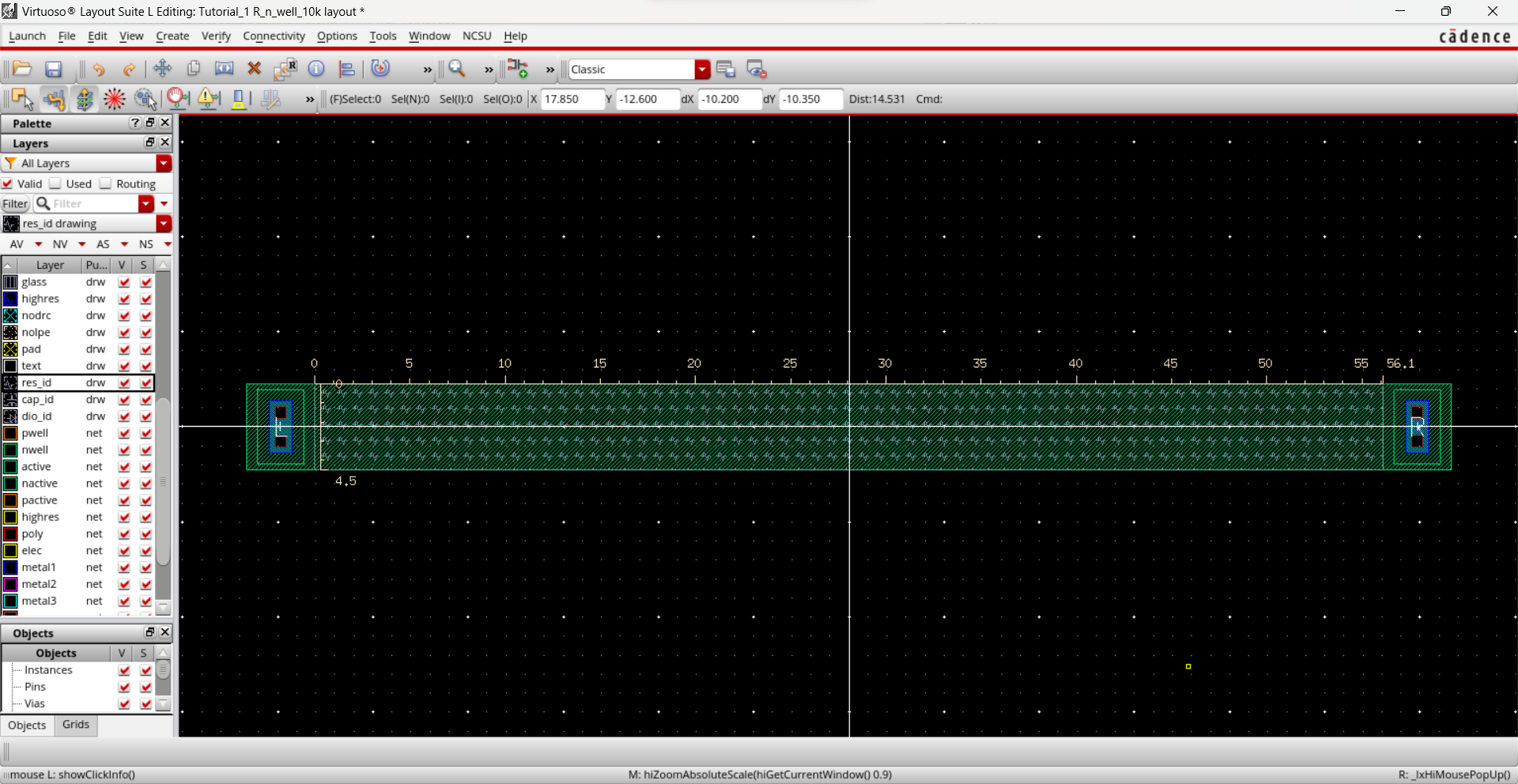
Using the keyboard shortcut "R", we can draw a rectangle to create our resistor. The formula R = Rsquare * L/W gives us the dimensions needed to achieve the desired resistance. A length of 56.1 and a width of 4.5 is selected to obtain a resistance of 10k ohms.
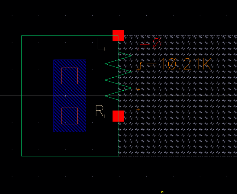
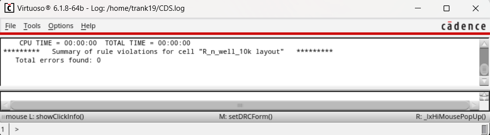
Extracting our layout shows us that the n-well restor we created has a resistance of 10.21k ohms. This is still within tolerance of our expected value as sheet resistance will vary.
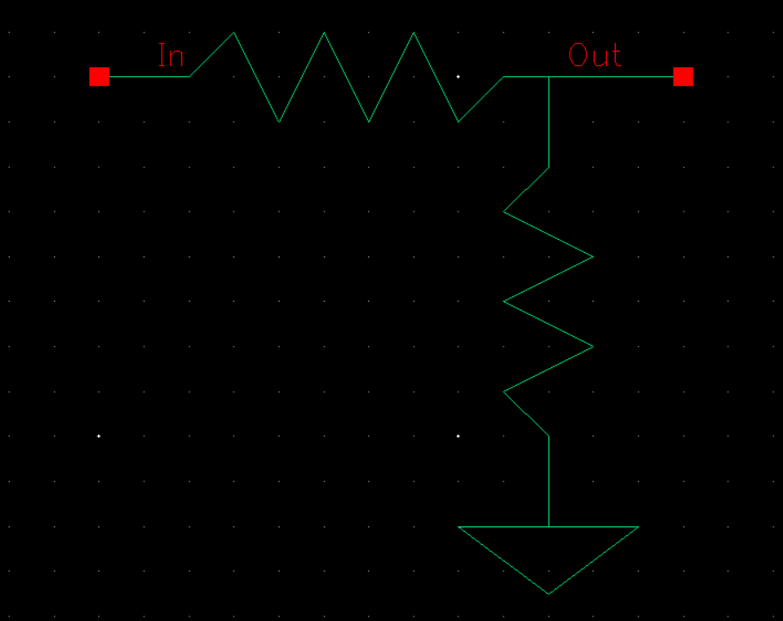
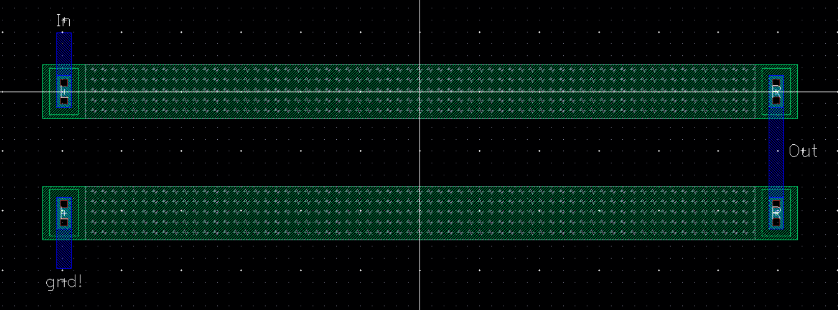
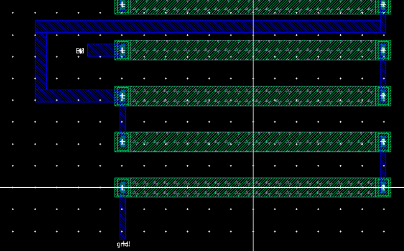
Once we had verified the resistance of the resistor we created, we can build our voltage divieder in a new layout using the metal1 layer to contect our contacts. We then create annd name 3 pins In, Out, and gnd!.
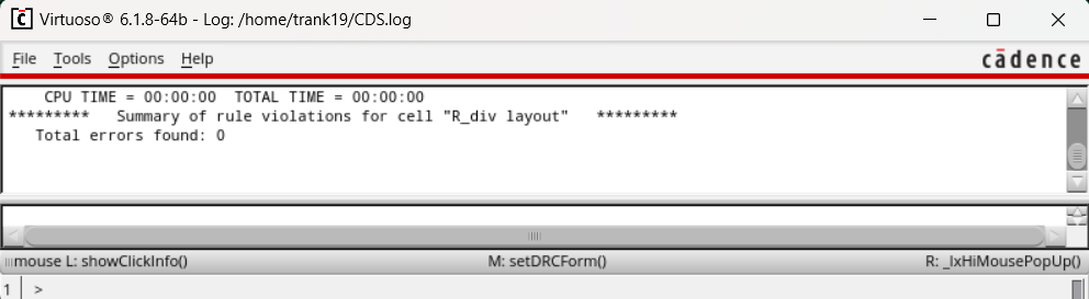
We then run a DRC to make sure there are no errors.
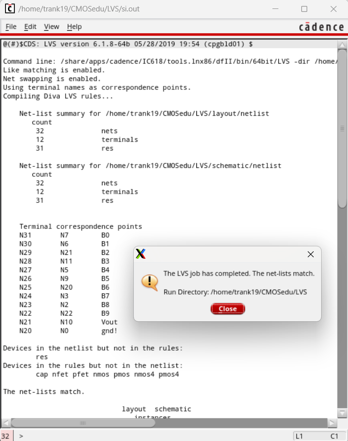
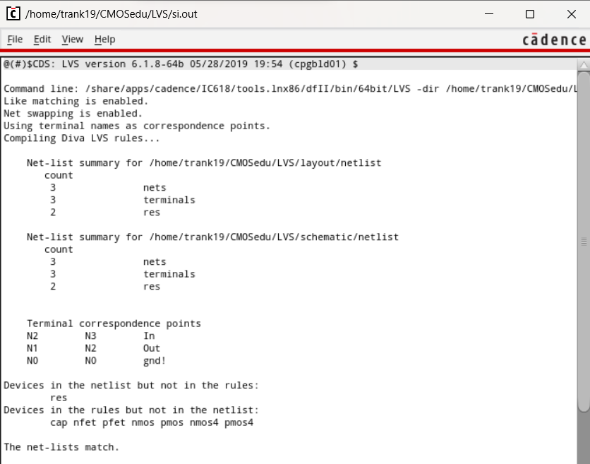
Once we had extracted our layout and varified that there are no errors from the DRC, we can run LVS and verify our netlists match.
We
will now use the 10k ohm resistor we constucted in Tutorial 1 to create
a 10-bit digital to analaog converter (DAC) according to a design we
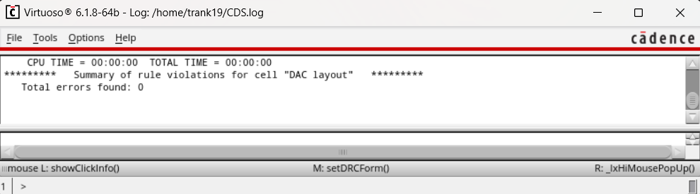
created in the previous lab. Below is the DRC for the single resistor
confirming we have no violations.
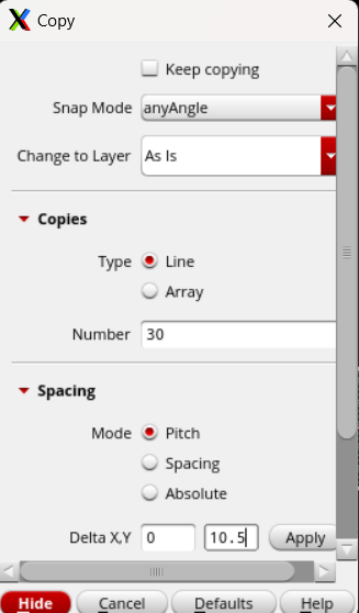
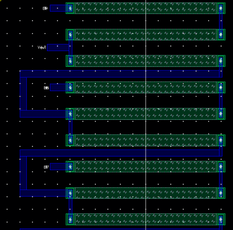
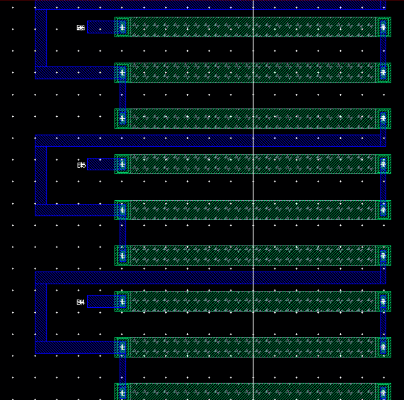
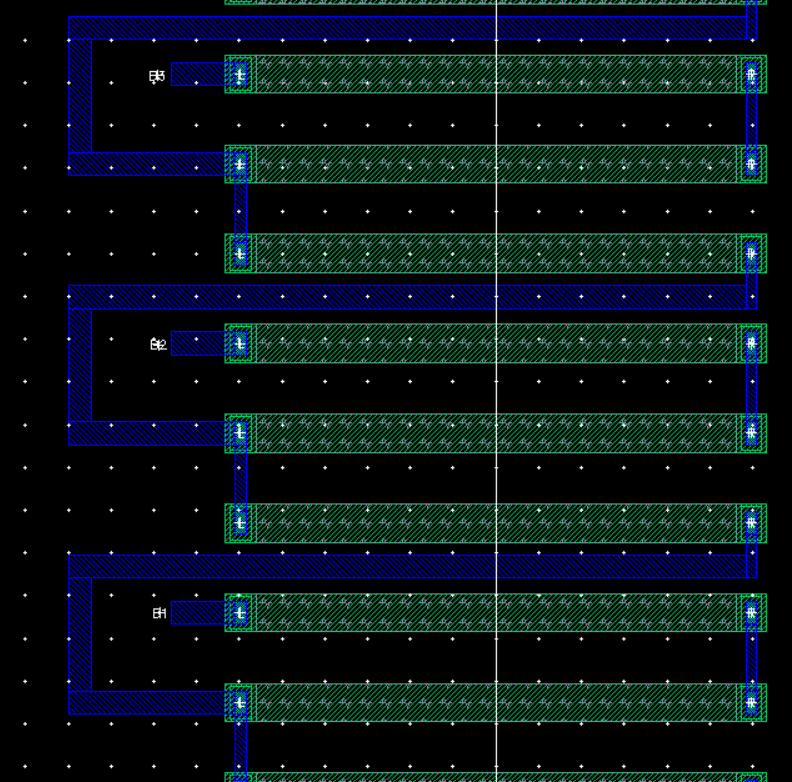
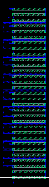
After placing 1 resistor in the new layout, we use the keyboard shortcut "c" to make 30 copies that are lined up with each other and evenly spaced far enough apart to meet the design contraints of the system.
Below is entire 10-bit DAC layout with all 31 resistors connected and pinned appropriately on the metal1 layer.
After constructing the layout, we run a DRC and confirm there are no violations.
With no errors found, we can now extract the layout before we run LVS.
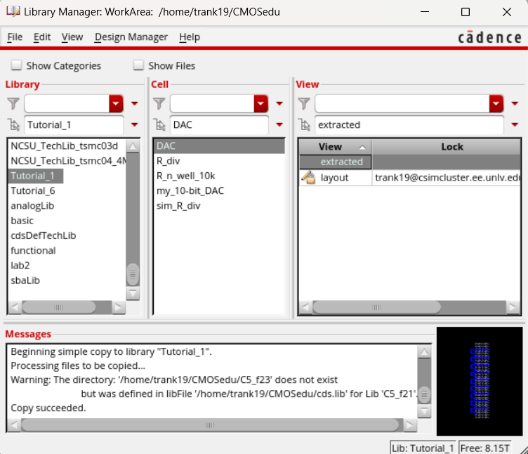
After successfully extracting the layout, we run LVS and are happy to report that the netlist matches. The 10-bit DAC layout is now complete.