Lab 1 - ECE 421L
Laboratory introduction, generating/posting html lab reports, installing and using Cadence
Pre-lab work
Prior
to the first day of lab, but no earlier than one week before the lab
starts, get a CMOSedu account, using your UNLV email address, from Dr.
Baker, rjacobbaker@gmail.com
Review the material seen here covering editing webpages (do this before the first lab)
Figure 1
This first lab will go through the first part of Tutorial 1.
(Go up to the 25th image in the tutorial)
1) Simply showing some of the images in this tutorial (that you generated) with some simple coherent narrative,
2) Discussing how you will do regular backups while working on the future labs by zipping up your work and emailing it to yourself or
uploading to dropbox, google drive, etc. with file names including the date (include at least two images to support your discussion).
Cadence Setup
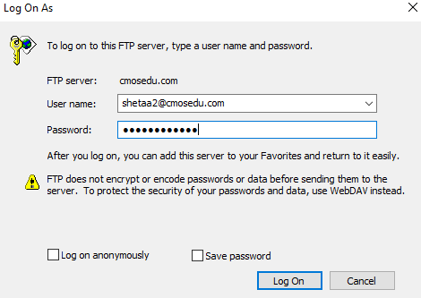
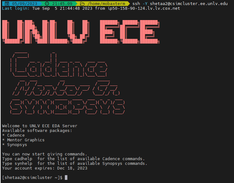
Logging into Cadence with the account provided by Dr. Greg
Deleting the
Building the Circuit
Creating a new library and configuring it with the correct settings (and the corresponding line created in the cds.lib file)
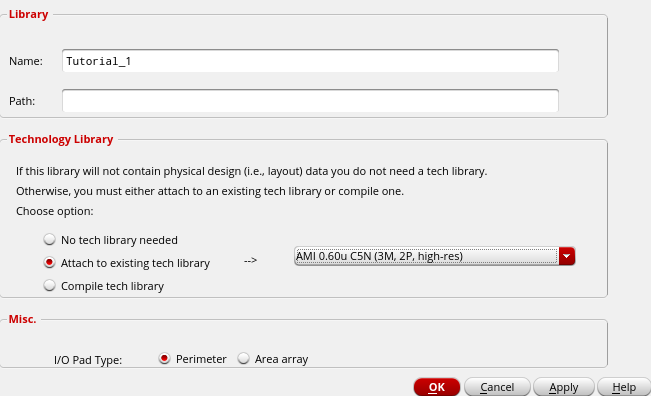
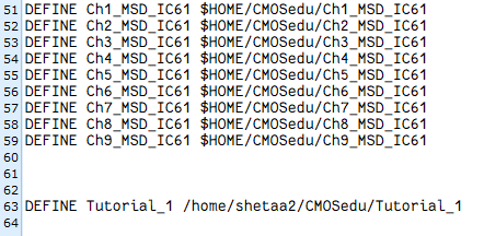
Figure 4 Figure 5
Creating the schematic and adding resistors
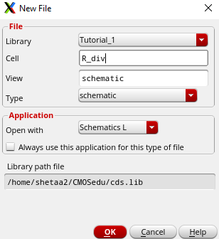
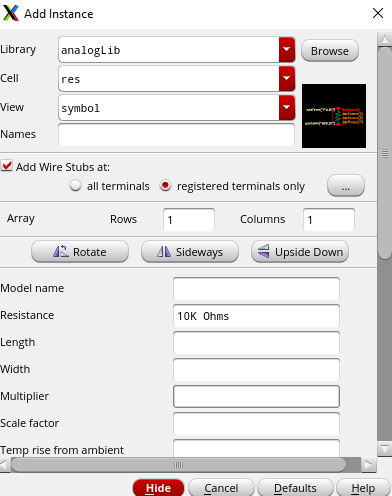
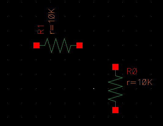
Figure 6 Figure 7 Figure 8
Here I will combine the steps of: adding ground and a 1-V DC source to the schematic, adding the wiring, & labeling wires
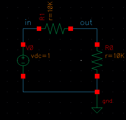
Figure 9
Simulating the Circuit
Setup for simulation (with spectre already selected)
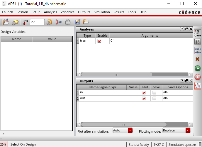
Figure 10
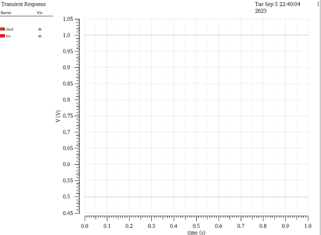
Results of the simulation
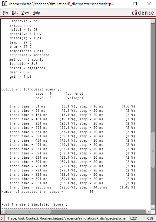
Figure 11
In order to backup my files and avoid redoing work that I have already done there are two ways I plan to protect my files.
Firstly I can backup my files by zipping them and emailing them to myself (as shown below) this is probably the safest thing to do however this is something that I could see myself forgetting to do here and there which is why I have another method I use as well. For this lab I zipped up my files about halfway through working on it and sent it to myself to avoid the risk of loosing my work.
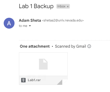
Figure 13
The second thing that I like to do is create a copy of my folder to work in if I am going to try anything that I am unsure about or could possibly be harmful to my work. For this first lab I created a copy of my lab folder to mess around with linking images and websites before I was confident enought to begin working on my lab submission.
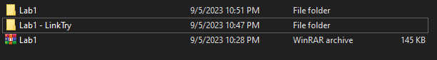
Figure 14