Lab 5 - ECE 421L
Backup:
Creating a backup for Lab 5 by emailing myself the zip files
Lab Purpose:
The purpose of Lab 5 is to design, layout, and simulate two different CMOS inverters.
The first inverter will have a PMOS/NMOS width size of 12u/6u. The length of both devices will be 0.6u.
The second inverter will have a PMOS/NMOS width size of 48u/24u. The length of both devices will be 0.6u.
Pre-lab:
1.) Go through Tutorial 3.
Pre-Lab Questions:
1. What does the Bindkey "q" do?
-The bindkey "q" brings up the properties window for schematics. This allows the user to change the properties of the instance values (e.g. resistance, voltage, capacitance, inductance, name, size, etc.)
2.) Which two Cell Views are used when doing an LVS?
-When doing a Layout vs. Schematic (LVS) check the two cells being compared are the schematic cell and the extracted cell. The extracted cell is produced from the layout cell.
3.) What is the difference between the nmos and nmos4 schematic cell?
-Nmos4 schematic cell has a fourth terminal apart from the Gate, Drain, and Source that can be set to the body or ground of the circuit, whereas the nmos schematic only has the Gate, Drain, and Source.
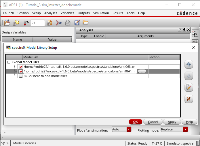
4.) How do you select the MOSFET models in the ADE window? What does ADE stand for?
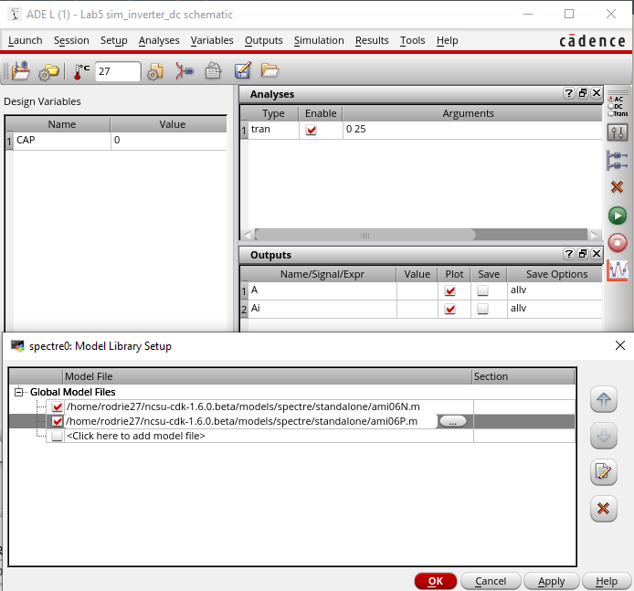
-To access the MOSFET models in the ADE window the user has to input the following steps in the tabs located at the top of the CAD: Launch -> ADE L -> Setup -> Model Library Setup. Then under Global Models click on the side to "add model file." From there in the "Choose Model File"go to the root directory and select the "ncsu-cdk-1.6.0.beta" folder -> models folder -> spectre folder -> standalone folder. For the PMOS/NMOS MOSFET we are using the file ami06P.m/ami06N.m files respectively. ADE stands for Analog Development Environment.
5.) What is the difference between moving and stretching?
-Using the move command lets the user move an instance around in the design process while use the stretch command lets the user elongate and change the dimensions of the instance.
6.) How do you layout a rectangle on the metal1 layer?
-In order to layout a rectangle on the metal1 layer the metal1 layer on the side panels must be chosen and then using the keybind "r" to produce rectangle for the metal1 layer.
7.) What does the ! indicate at the end of the gnd! and vdd!
-Using ! at the end of gnd and vdd indicates a global variable, which lets the variable be recognized in a different hierarcy to other variables.
8.) What do the acronyms LSW and CIW stand for?
-LSW stands for Layer Selection Window and CIW stands for Command Interpreter Window
9.) How is the ruler used? Cleared?
-The ruler is used by pressing the "k" bindkey within the selected CAD window. By pressing the "esc" key the user can exit the ruler and by pushing the "delete" button and clicking on the ruler measurements the user can clear out labels. A second method of clearing the ruler is by pressing "shift-k."
The tutorial then hads us go through the process of creating an inverter.
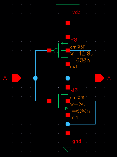
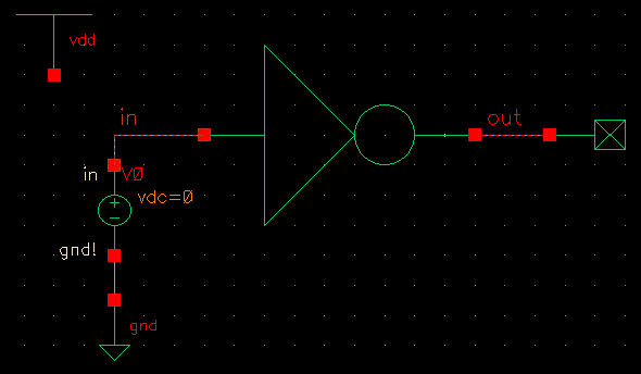
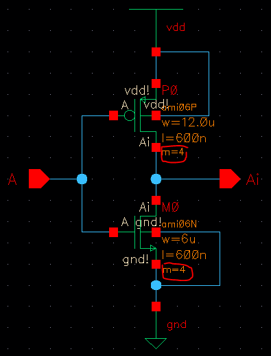
To create the inverter I connect an PMOS with 4 terminals in series with a NMOS with 4 terminals. A voltage, vdd, is connected to the drain and bulk of the pmos and the source is connected to the drain of the NMOS and to the output Ai of the inverter. The NMOS's source is connected to the ground. Both the PMOS and NMOS gates are connected to the input, A.
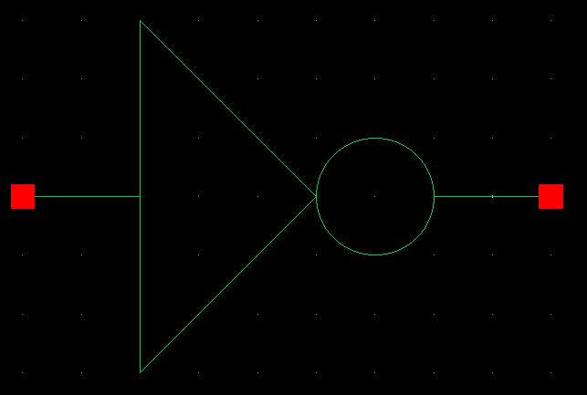
The next step within the tutorial is to create the symbol for the inverter after running check and save on the schematic with no errors.
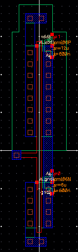
After creating the symbol for the inverter the next step is to create the layout of inverter using the nmos, pmos, ntap, ptap, and m1_poly cells.
The dimensions used for the NMOS are 6u/0.6u and for the PMOS it's 12u/0.6u. The ntap and ptap use two columns as dictated per the tutorial.
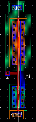
I then run a DRC check on the layout in order to verify there design is correct.
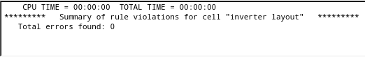
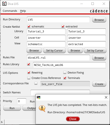
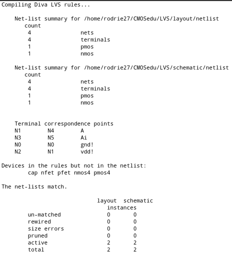
I then extract the layout in order compare the layout and schematic with a LVS check.
The LVS shows that there the netlist match for botht the layout and schematic
The next step within tutorial is to place the newly created inverter within a circuit to test its properties and make sure it is functioning properly.
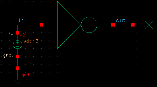
The inverter circuit is connected to a voltage, vdc, and an output connected to a no-connection symbol.
The next step is to select the model files for the ami06 NMOS and PMOS that are within the inverter symbol.
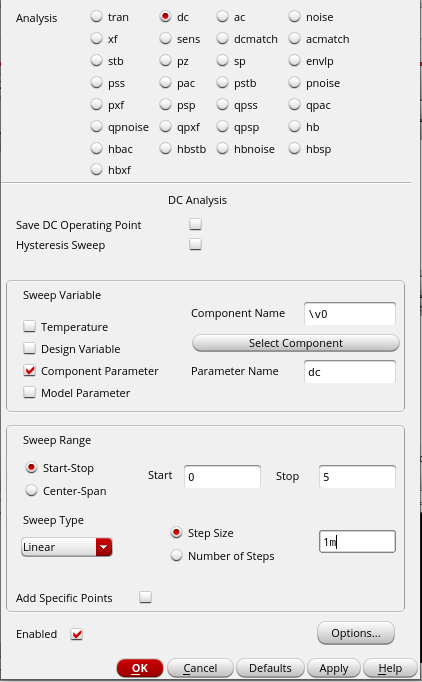
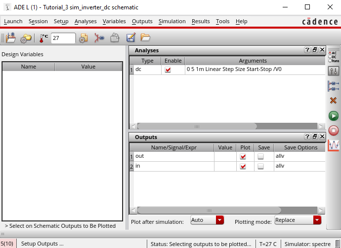
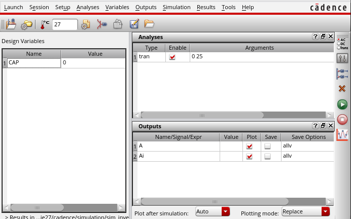
After adding the NMOS and PMOS to the model library setup the next step is to run the analyses on the inverter circuit.
Before plotting out the results from the "out" node and "in" node have to be selected on from the tab Outputs -> To Be Plotted -> Select on Design.
Since there is no vdd variable added to the inverter circuit the output voltage on the graph is 0 V. This means a vdd source has to be added to the circuit.
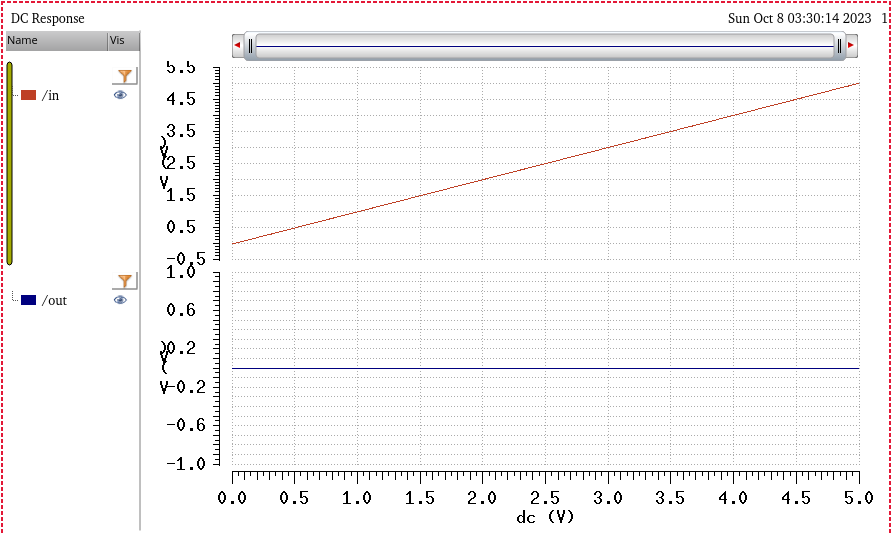
Adding the vdd allows the circuit to properly produce the response from the inverter circuit.
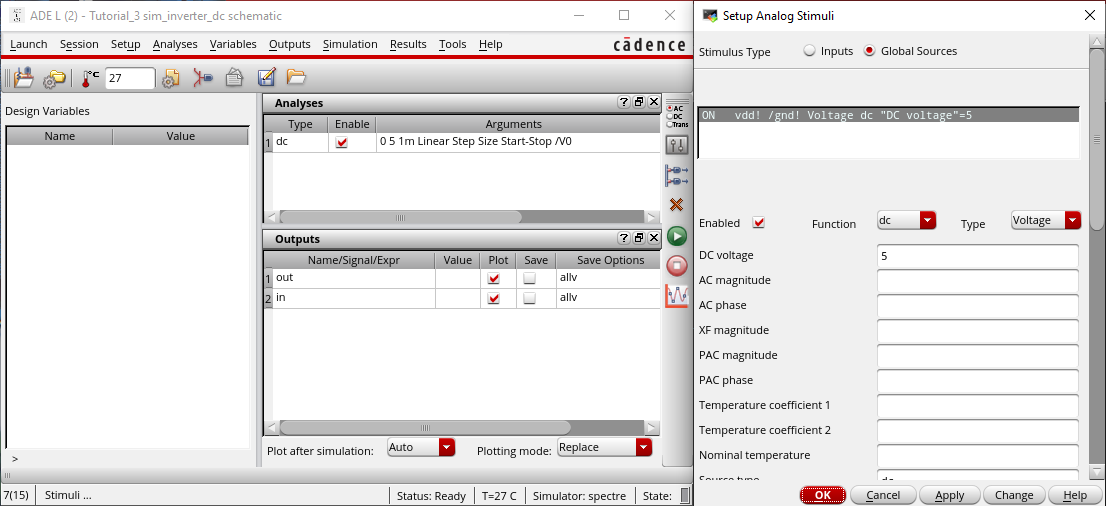
The added vdd! acts like a global "plower supply" so adjustments need to be made within ADE. Selecting Setup -> Stimuli and changing the parameters within the Global Sources.
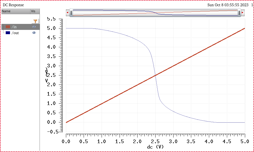
Running the analyses on the inverter circuit with the global vdd! produces the proper inverter voltage transfer curves.
The next step is to simulate the extrated layout via the ADE by selecting the tabs Setup -> Environment and adding "extracted" before "schematic" within the "Switch View List" line
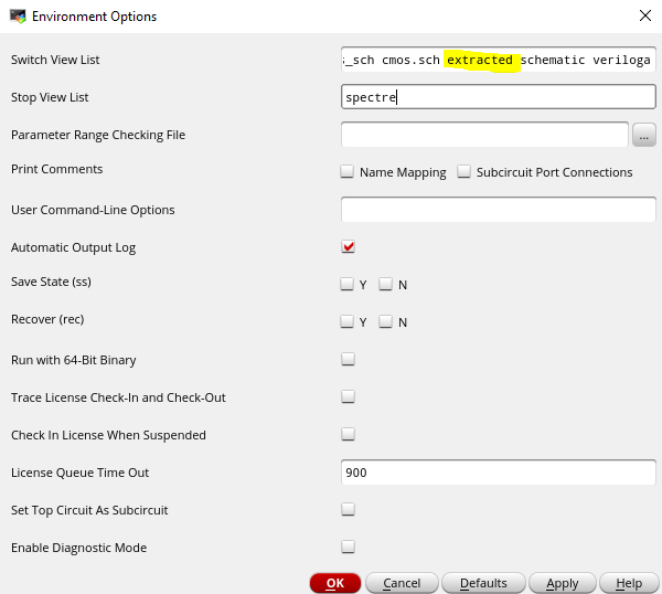
After running the simulation again we can see that the output results of the extracted layout are the same as the schematic. To verify that we are looking at the extracted view we click on Simulations -> Netlist -> Display.
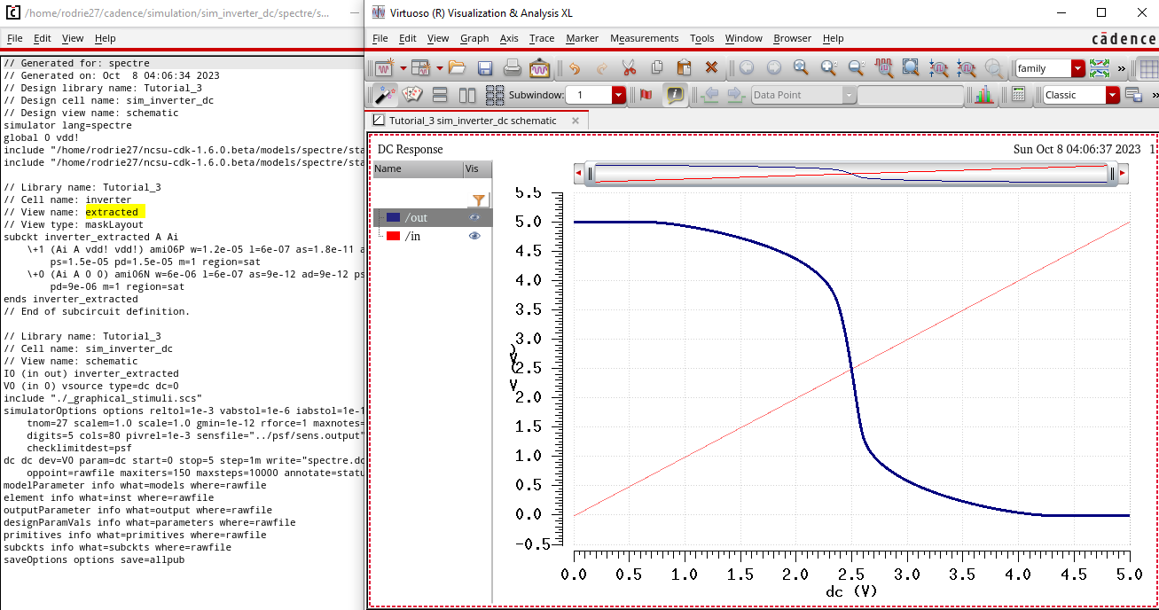
By verifying that the voltage transfer curves of the schematic and extracted layout are the same we conclude the tutorial 3 for lab 5.
Lab 5: Design, layout, and simulation of a CMOS inverter
Experiment 1: Schematic, Layout and Symbol for 12u/.6u PMOS and 6u/.6u NMOS
From the pre-lab, we create the 12u/6u inverter schematic
Then the next step is to create the symbol for 12u/6u inverter
After the symbol for the inverter is created we move onto the layout of the inverter
Once the layout for the 12u/6u inverter is completed we DRC check to make sure there are no errors. Once there are no errors the layout is extracted and I run an LVS check to make sure the schematic matches the layout.
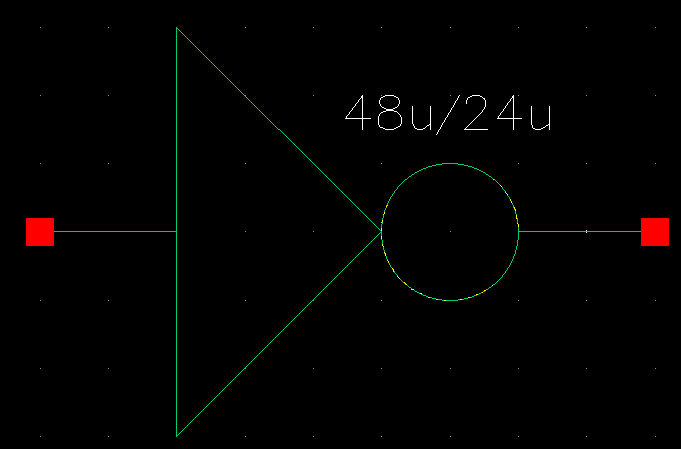
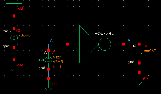
Experiment 2: Schematic, Layout and Symbol for 48u/.6u PMOS and 24u/.6u NMOS
The next step is create the 48u/24u inverter, using the inverter created in the prelab and expanding the size using "m = 4" multiplier for both the PMOS and NMOS.
The next step is to create the symbol for the 48u/24u inverter
Once the symbol is created I can move on to creating the layout view and extracted view for the 48u/24u inverter
Running a Layout vs Schematic (LVS) check shows that the net list match.
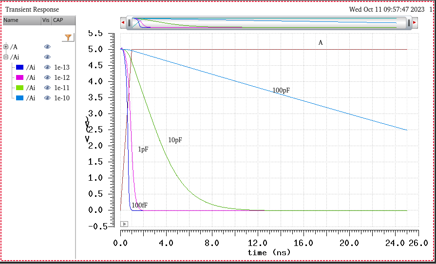
Experiment 3: Simulation for the 12u/6u inverter
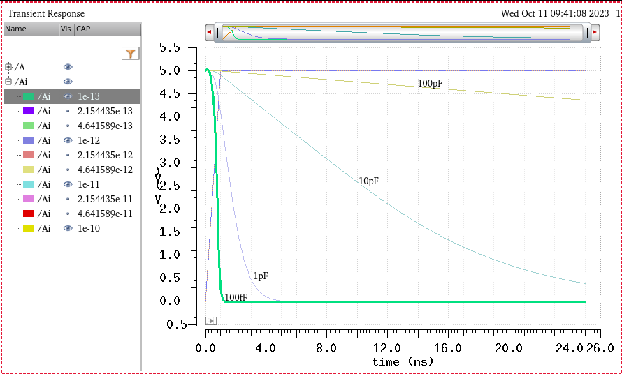
The next part of the lab is to simulate the 12u/6u inverter within a circuit driving 100 fF, 1 pF, 10 pF, and 100 pF capacitive load.
To do this I set the inverter symbol within the circuit with output being the capacitive load.
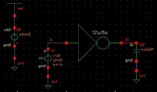
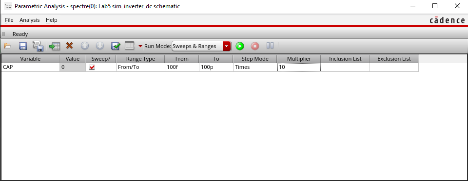
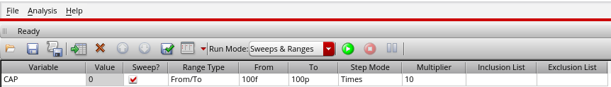
I set the capacitor output variable to "CAP" so I can run a parametric sweep on the variable itself
Afterwards, I simulate the circuit through Ultrasim. This results of the Spectre simulation and Ultrasim simulation match each other.
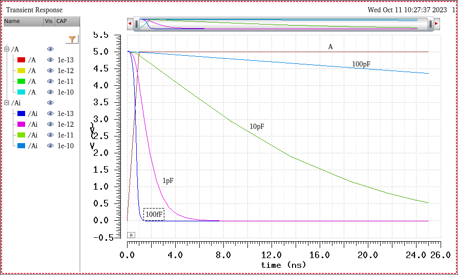
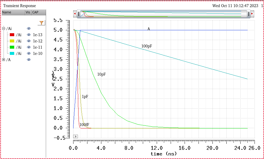
Experiment 4: Simulation for the 48u/24u inverter
Once more, we simulate the circuit this time it's the 48u/24u inverter with a it being driven with a 100 fF, 1 pF, 10 pF, and 100 pF capacitive load.
Once more seting the capacitor output variable to "CAP" so I can run a parametric sweep on the variable itself
Like before I run a parametric analysis on the driving output capacitance value for 100 fF, 1 pF, 10 pF, and 100 pF
Conclusion
A higher capacitance will result in a slower transition for the output. The change in output is dampened for higher capacitance values.
The 48u/24u inverter caused the output to transition quicker due to the fact that the resistance of a larger MOSFET is lower.
On the other hand, the 12u/6u inverter caused the output to transition lower since the resistance of this smaller MOSFET is higher.
The time delay is directly influenced by the resistance value which means that a higher resistance will result in a higher time delay and vice versa.
This concludes lab 5.
My zip files for this lab can be downloaded here.