Lab 8 - ECE 421L
Authored
by Baylee Perera, pererb1@unlv.nevada.edu; Kolby Tran trank19@unlv.nevada.edu; Josue Magana Quezada maganaqu@unlv.nevada.edu
December 6, 2023
Generating a test chip layout for fabrication; Chip2_f23
Prelab:
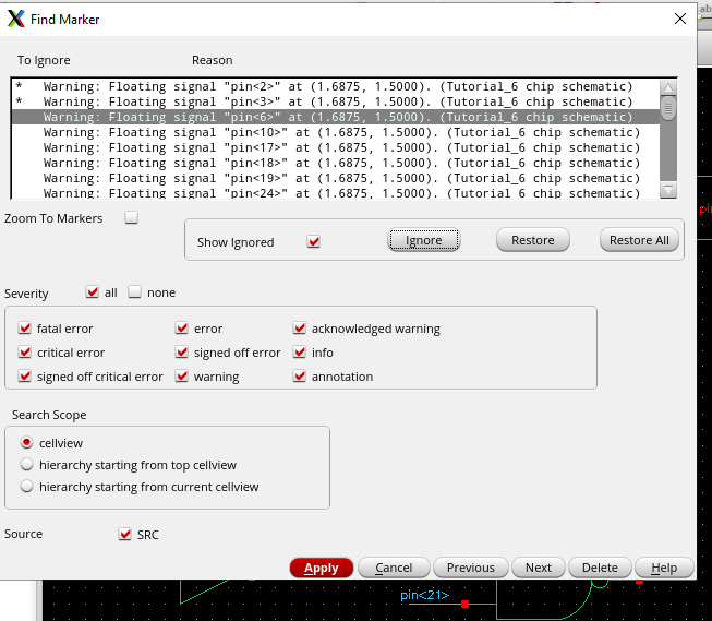
For this prelab, we will be going back to Tutorial 6 and completing the steps in it. This will help us with designing our chip.
Lab description:
In
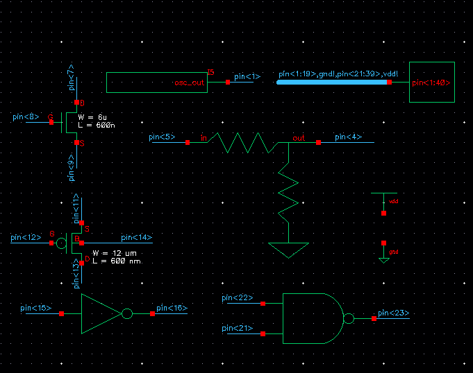
this lab, we will be designing a test chip layout. Our lab will include the following:
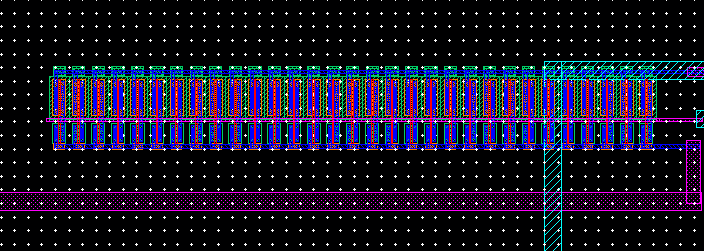
- A 31-stage ring oscillator with a buffer for drivinig a 20 pF off-chip load.
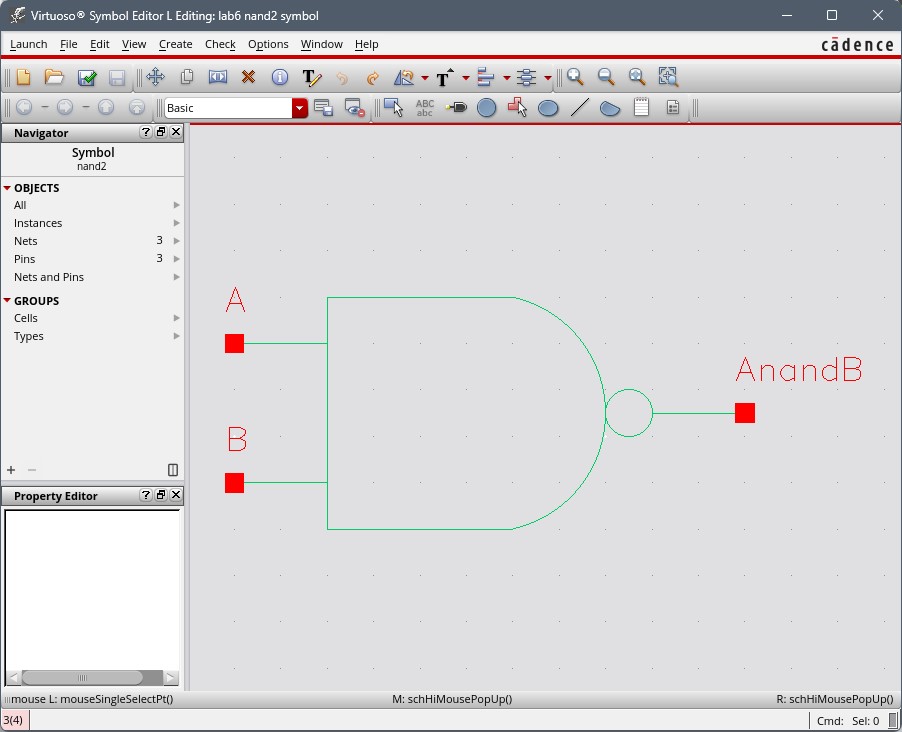
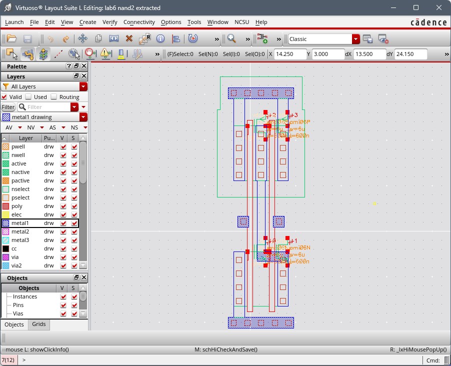
- NAND and NOR gates using 6/0.6 NMOSs and PMOSs.
- An inverter made with a 6/0.6 NMOS and a 12/0.6 PMOS.
- Transistors,
both PMOS and NMOS, measuring 6u/0.6u where all 4 terminals of each
device are connected to bond pads (7 pads + common gnd pad).
- Using
the 25k resistor laid out below and a 10k resistor implement a voltage
divider (need only 1 more pad above the ones used for the 25k resistor).
- A 25k resistor implemented using the n-well (connect between 2 pads but we also need a common gnd pad).
- Simple
explanation on how to test each test structure, with simulations (e.g.
What inputs should be given to the circuit? What pin numbers on the
chip should the user connect to?),
- Top level cell chip
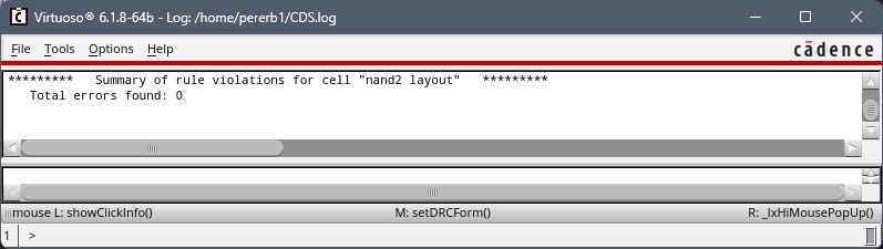
schematic + layout that is DRC/LVS clean [if available] and adheres to
the instructions given (circuits cannot share power, GND pin is pin 20,
etc).
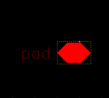
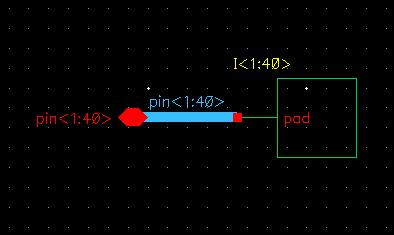
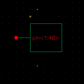
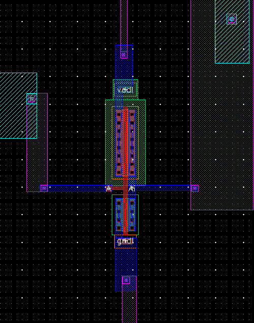
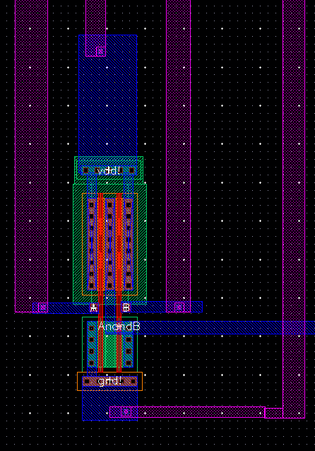
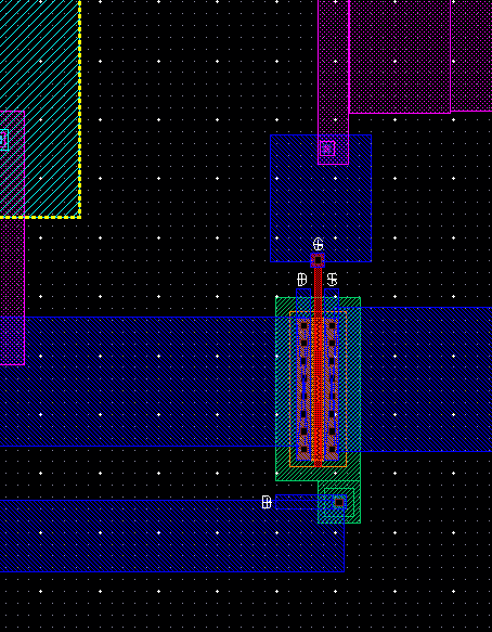
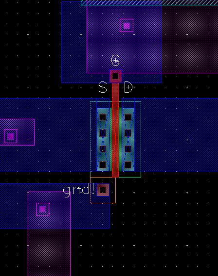
Components:
| Schematic | 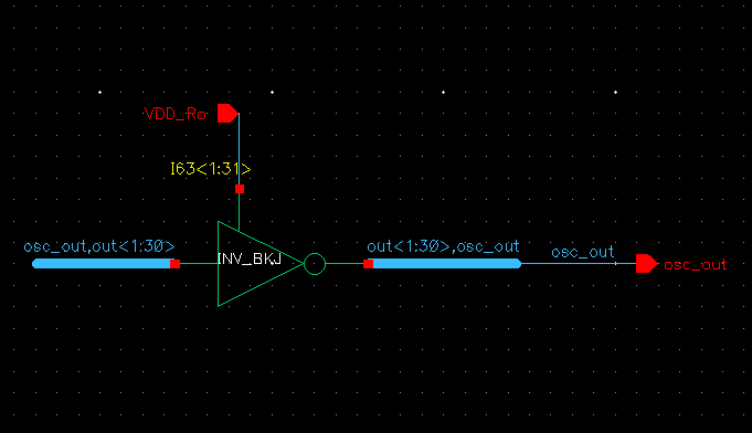
|
| Symbol | 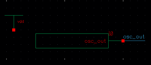
|
| Layout | 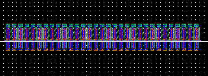
|
| Schematic | 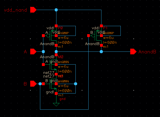
|
| Symbol | 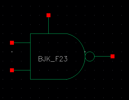
|
| Layout | 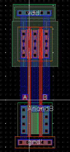 |
| Schematic | 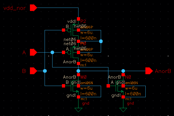 |
| Symbol | 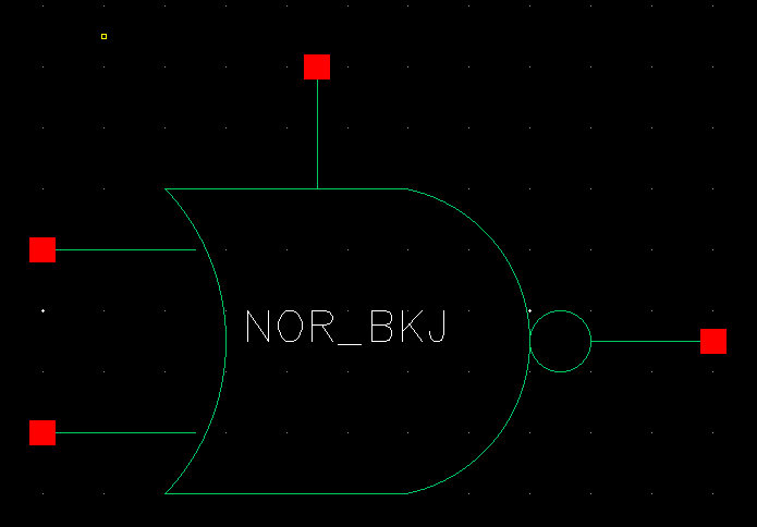 |
| Layout | 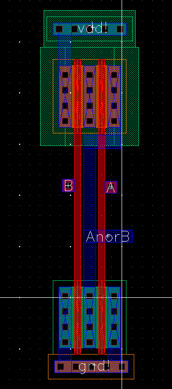 |
| Schematic | 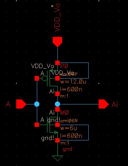 |
| Symbol | 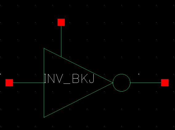 |
| Layout | 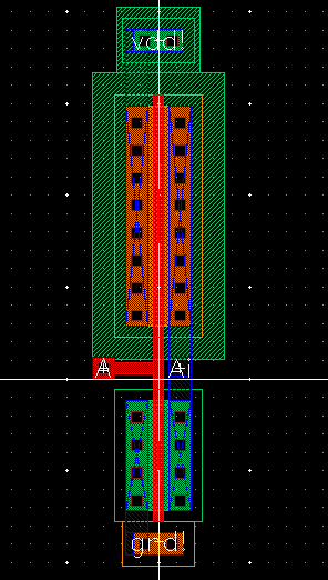 |
| Schematic | 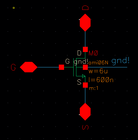 |
| Symbol | 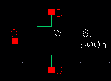 |
| Layout | 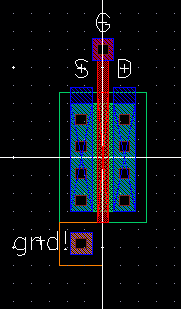 |
| Schematic | 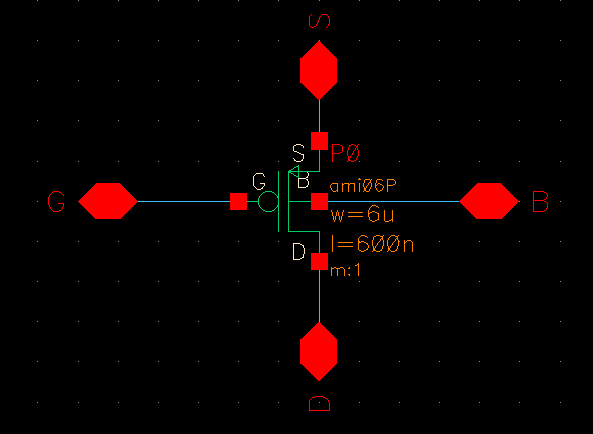 |
| Symbol | 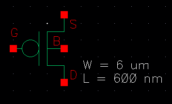 |
| Layout | 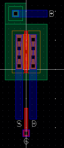 |
| Schematic | 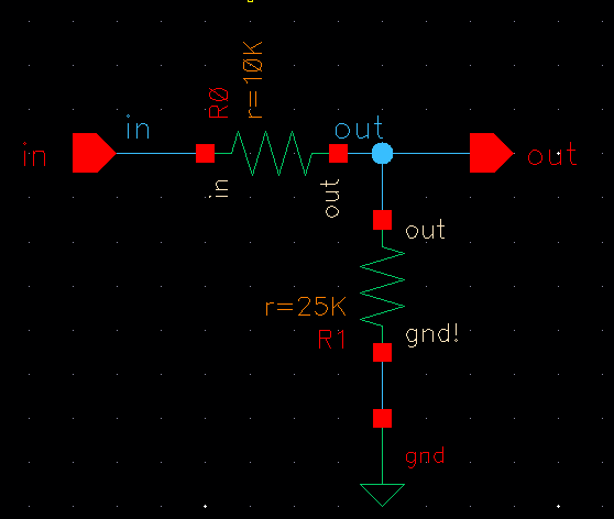 |
| Symbol | 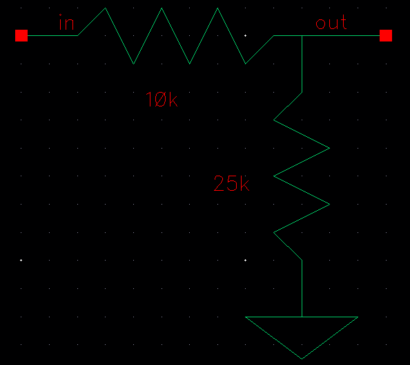 |
| Layout | 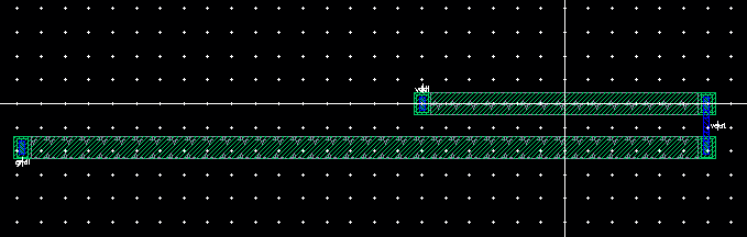 |
Chip:
| Non-inverting Buffer Schematic | 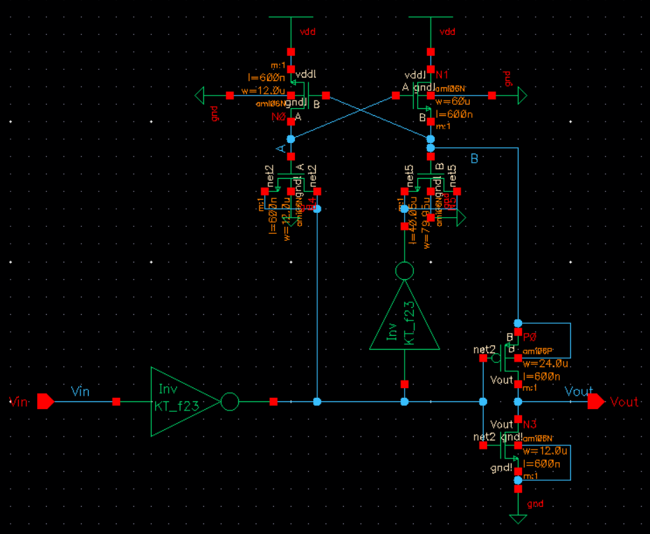 |
| Non-inverting Buffer Symbol | 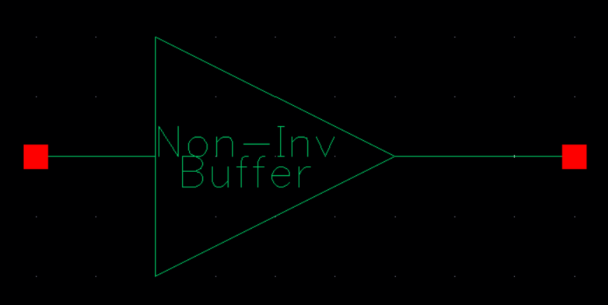 |
| Non-inverting Buffer Layout | 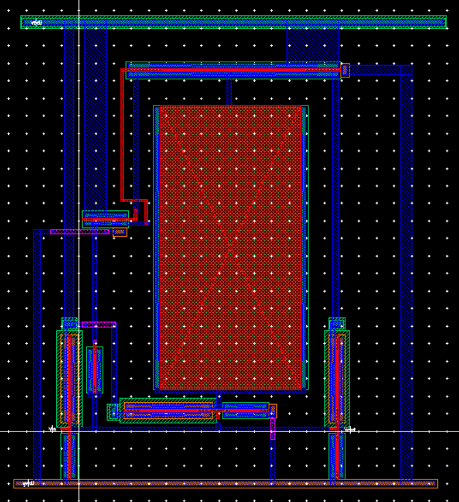 |
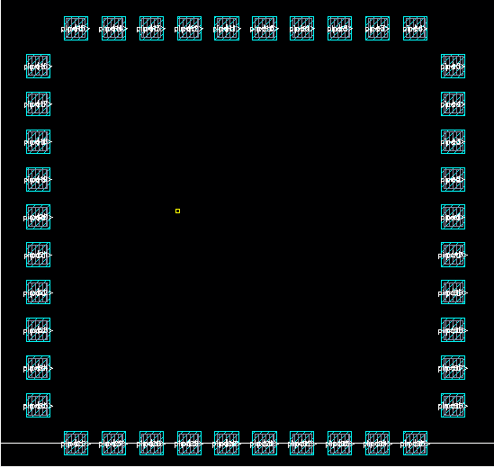
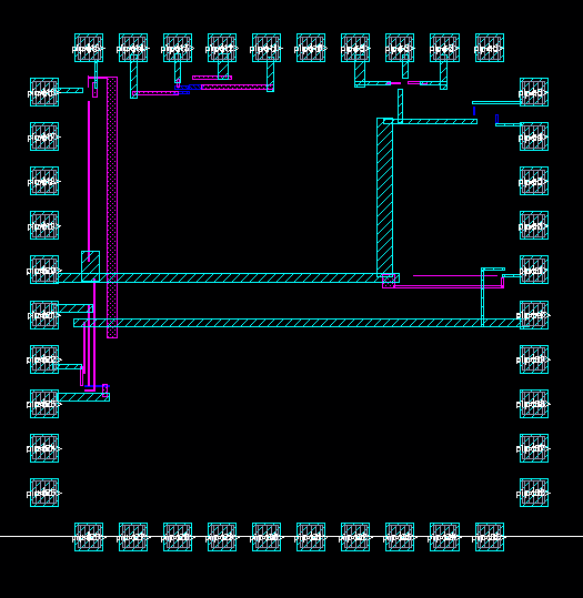
| Chip Layout | 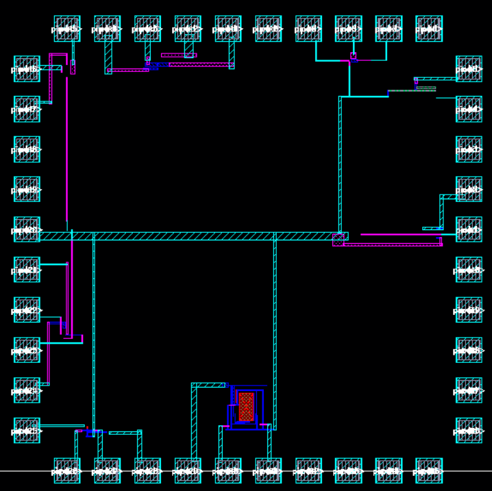 |
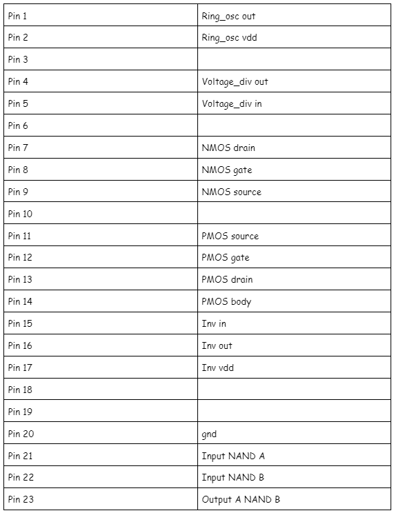
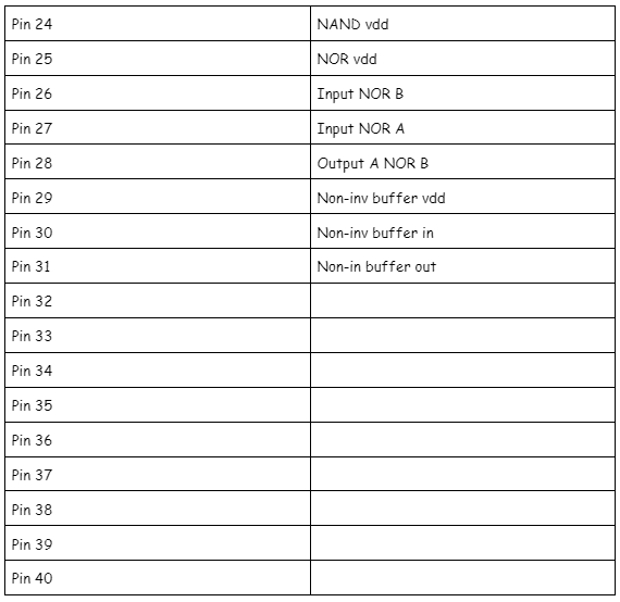
Pin Out Table:
Lab backups:
Chip2_f23
Return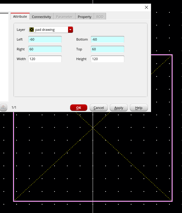