Lab 5 - ECE
421L
Design,
layout, and simulation of a CMOS inverter
|
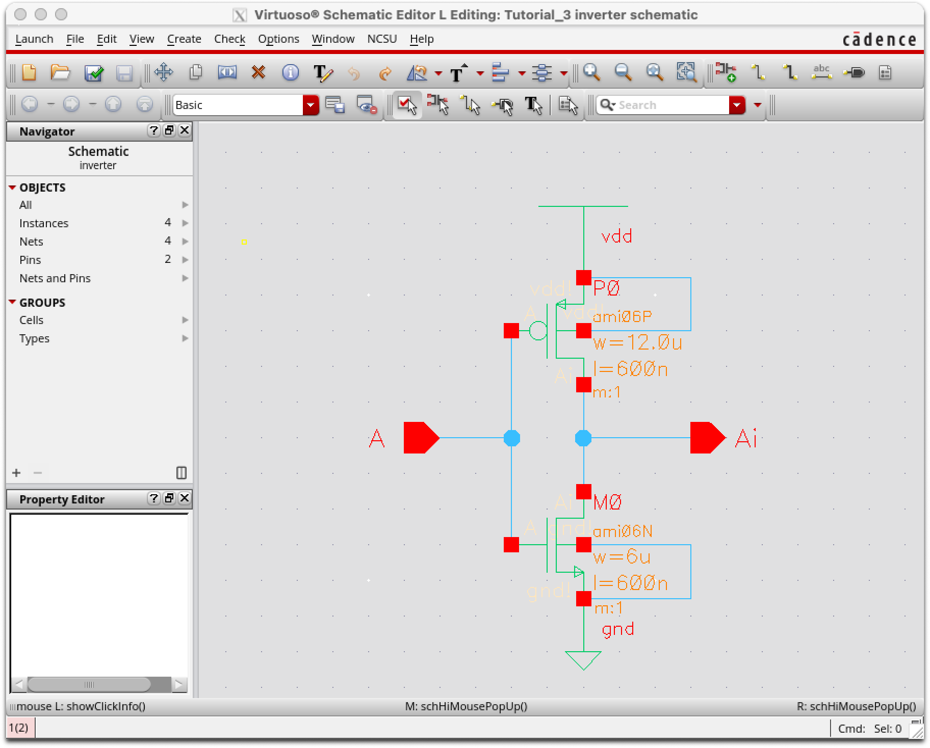
Schematic of inverter using NMOS and PMOS |
|
|
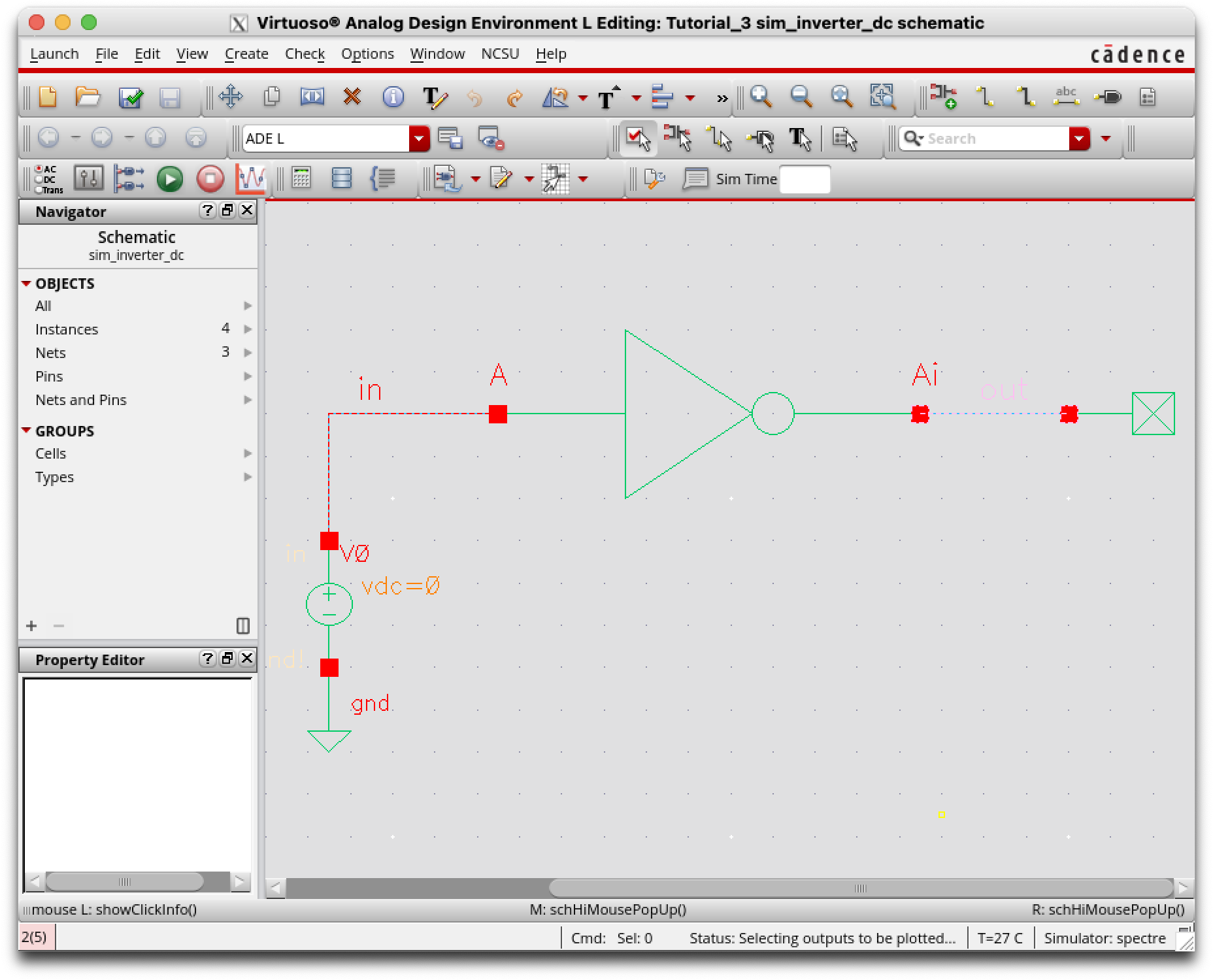
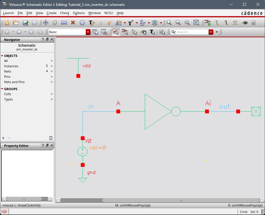
Schematic of inverter in use. Using a handmade
symbol. |
|
|
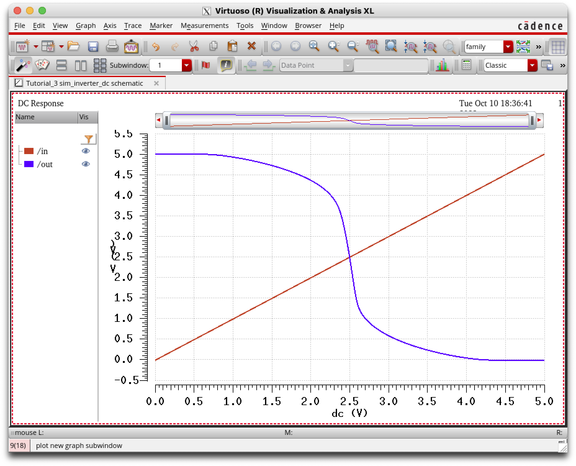
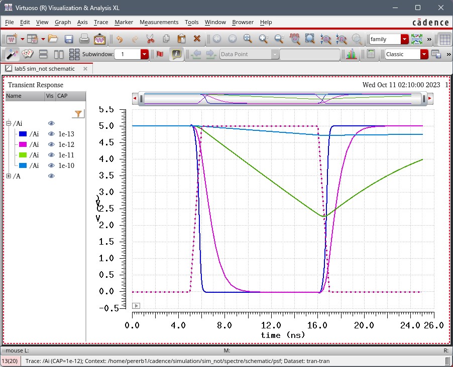
Out of the inverter compared to input. |
|
|
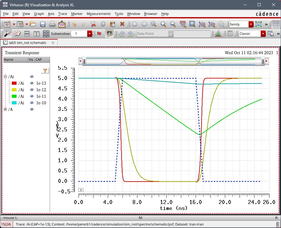
Extracted view output vs input simulation. |
|

Lab Process:
| 12u/6u Inverter Schematic |  |
| 12u/6u Inverter Symbol | 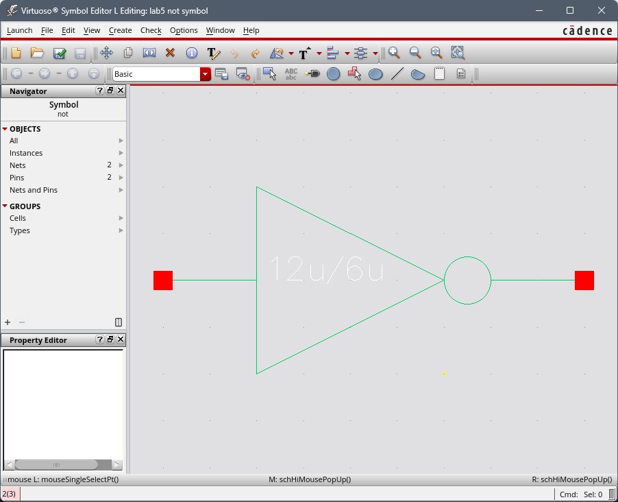 |
| 12u/6u Inverter Layout |  |
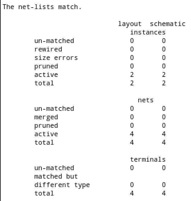
| Checking that Extracted View and Schematic pass LVS |  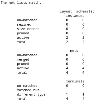 |
48u/24u Inverter Schematic 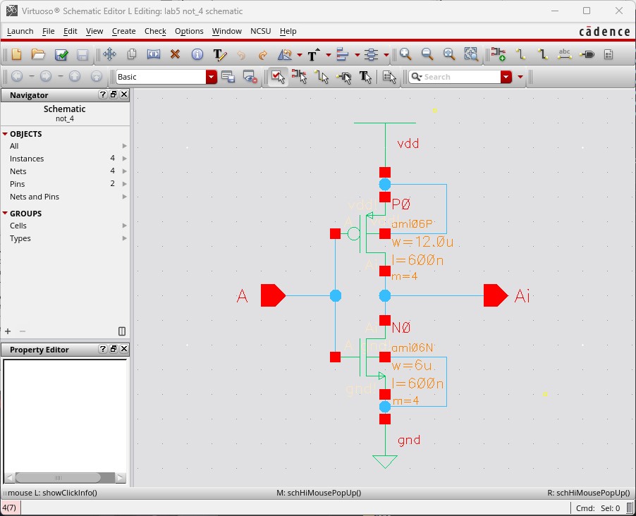
48u/24u Inverter Symbol 
48u/24u Inverter Layout 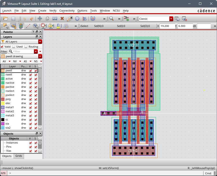
Checking that Extracted View and Schematic pass LVS 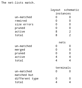
Capacitance Sweep: Schematic: Spectre Simulations Ultrasim Simulations 100fF, 1pF,
10 pf, 100 pF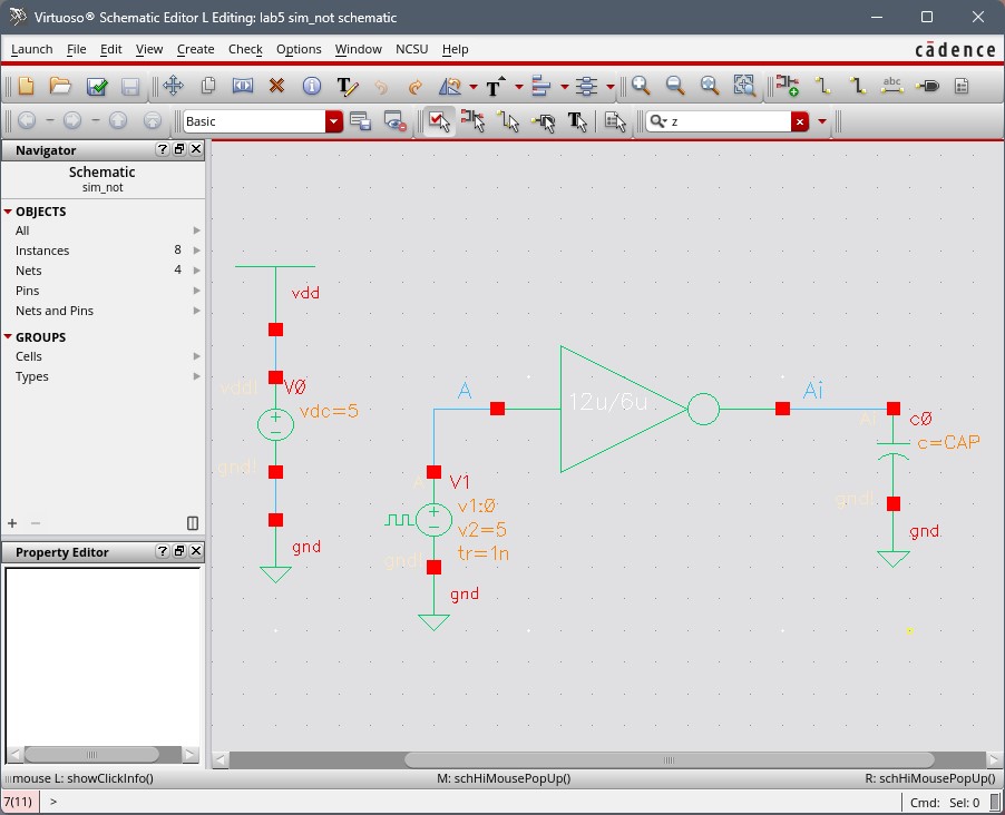
Same process like the previous one.
| Capacitance: | Schematic: | Spectre Simulations | Ultrasim Simulations |
| 100fF, 1pF, 10 pf, 100 pF | | | |
Conclusion:
When there is a higher capacitor load, the transition on the output is going to slow down. As we can also see from out lab data, the 48u/4u inverter ended up having a faster transition. This is due to it's increased size which then decreases the resistance.
Cadence files: here
Proof of backed up lab: