Lab 03 - EE 421L Fall 2023
Authored
by
Baylee Perera; pererb1@unlv.nevada.edu
9/20/23
Design of a 10-bit digital-to-analog converter (DAC)
Backups:


Prelab:
The prelab continues to work through tutorial 1 that we started back in lab 1. Please refer to my lab for steps.
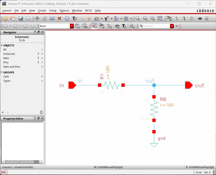
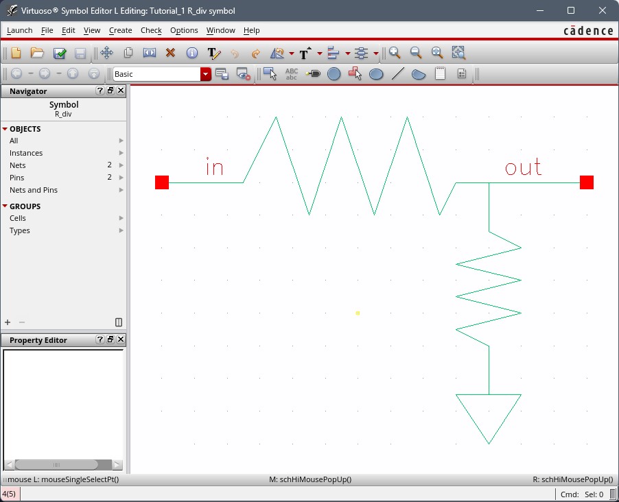
We started off by turning our schematic into a symbol.
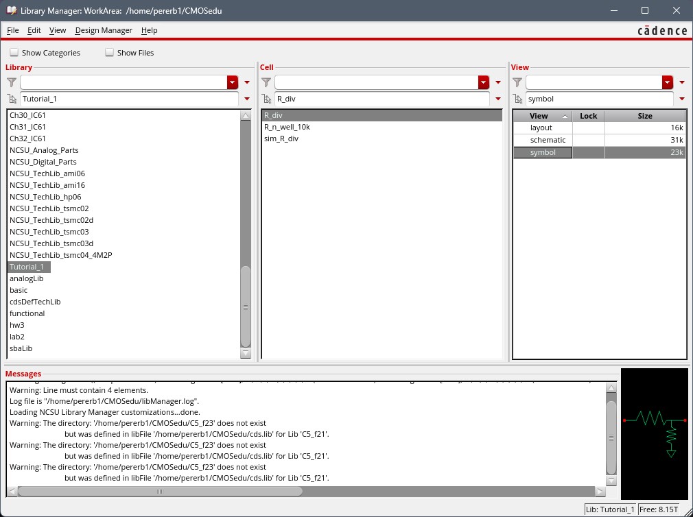
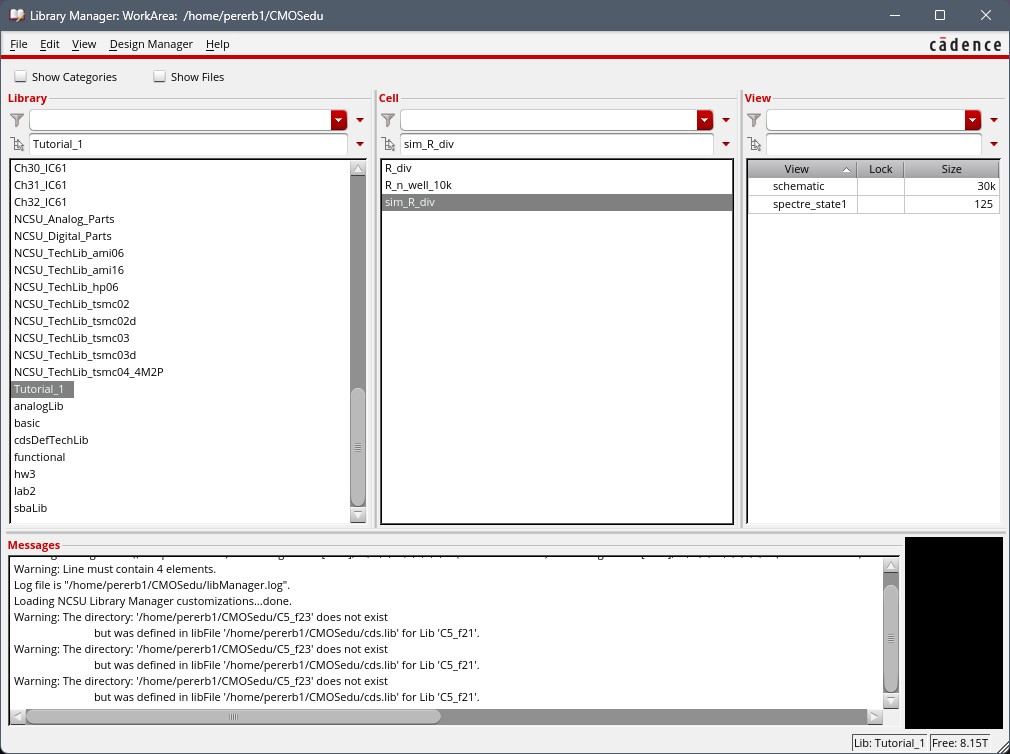
We
then copied the cell and renamed it sim_R_div. Which we then deleted
the spectre save from R_div. This allows us to use the symbol in
sim_R_div.
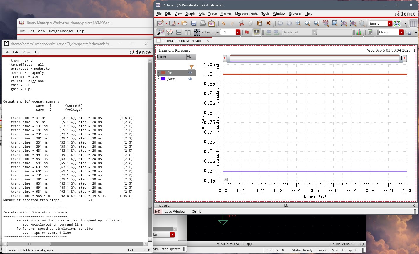
We eventually turned out symbol that we made into a circuit, then proceeded to run the simulation.
The
next step was to make our layout and call it R_div. We then used
rectangles while selecting the correct layers to draw our resistor. We
were able to obtain this by using the formula R = Rsquare * L/W. Since this tutorial called for a 10k resistor, we did a width of 4.5 and a length of 56.1.

Below is my extracted layer to verify we got our desire resistor.
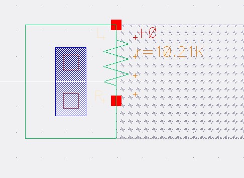
Once that is done, we build our voltage divider. The labels are there for Vin, Vout and ground.
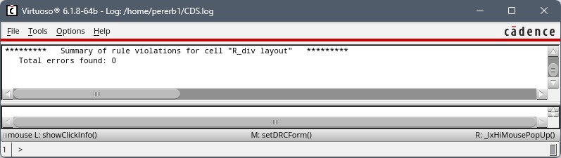
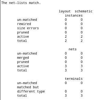
Once
that is built, we run both DRC and LVS on our layout and schematic to
make sure there are no error and for netlists to match up.
Lab Work:
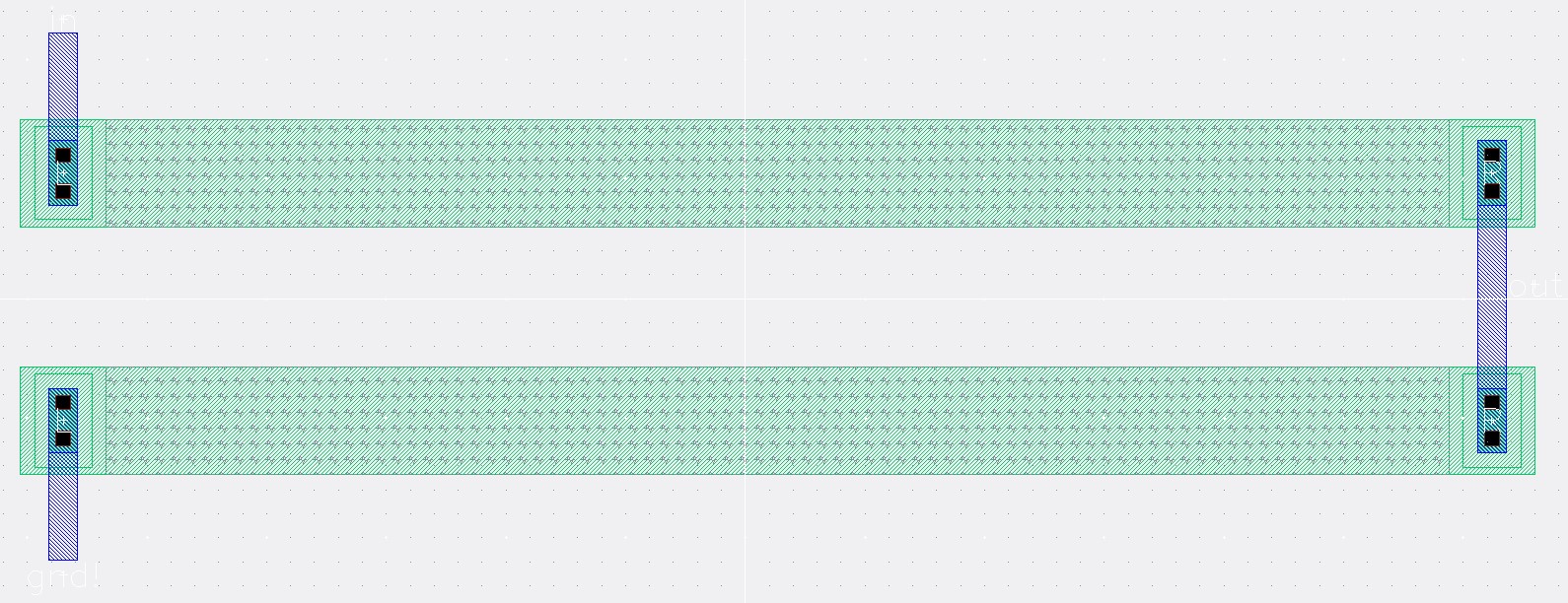
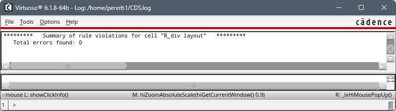
This
lab asked us to make a 10-bit DAC using the 10k resistor we made. The
dimension info is found above in my prelab portion. To verify, I have
attached again the screenshot of the DRC for the resistor.

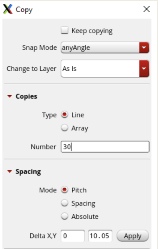
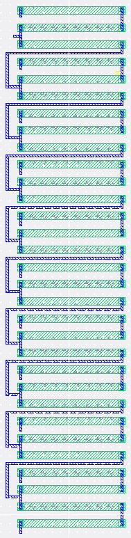
The
next step is to place down 30 of our one resistors using the copy
command which is just 'c'. 30 was chosen because it must be divisible
by 0.15um in order to meet the constraints.
We follow the same process with our metals that we used to place out the resistor.
Once everything is laid out, we then connect all the pins together.
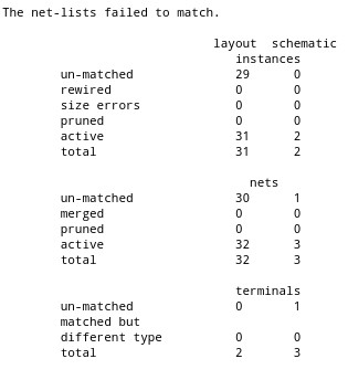
We
again run both DRC and LVS to ensure no errors and the netlists match
(my LVS didn't match but I think it's because I forgot to label).
tutorial_1.zip
Return to previous labs