EE 421L Final Project
Part 2 procedures:
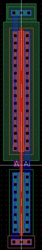
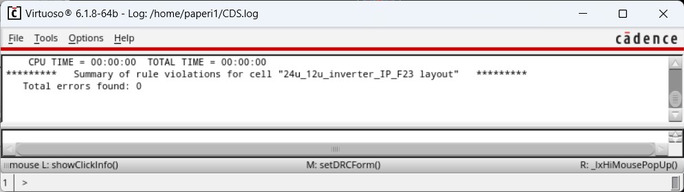
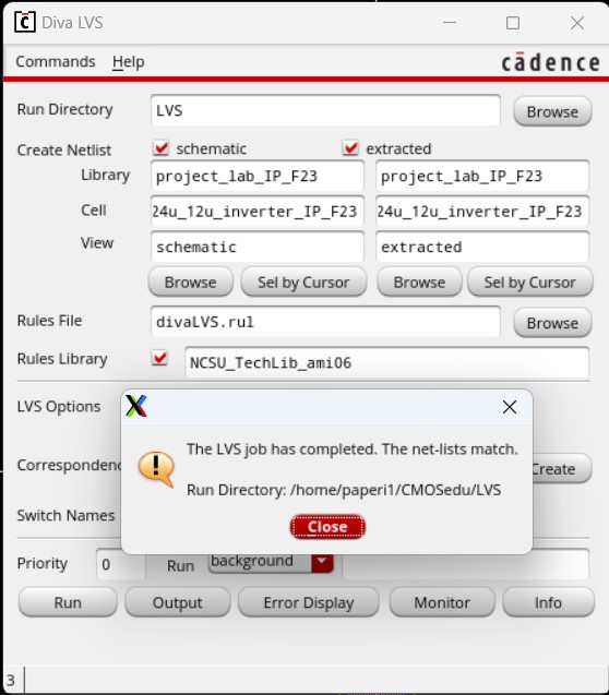
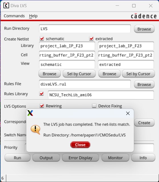
I started by laying out the 24u/12u inverter, to later be used in the non-inverting buffer layout, and verified it with DRC. Then I extracted the layout and ran LVS verification, looking for a match.
| |
| |
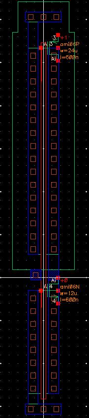
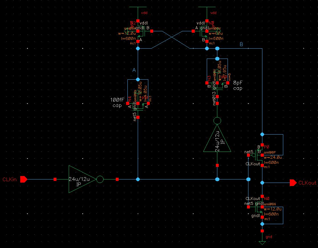
Moving on to the complete layout, two of these inverter layouts were used as well as four separate NMOS layouts and another separately created inverter. There are four pins in this layout—input CLKin, output CLKout, inputoutput vdd! and inputoutput gnd!—as well as two labels (A and B) that correspond with the same labeled wires in the schematic.
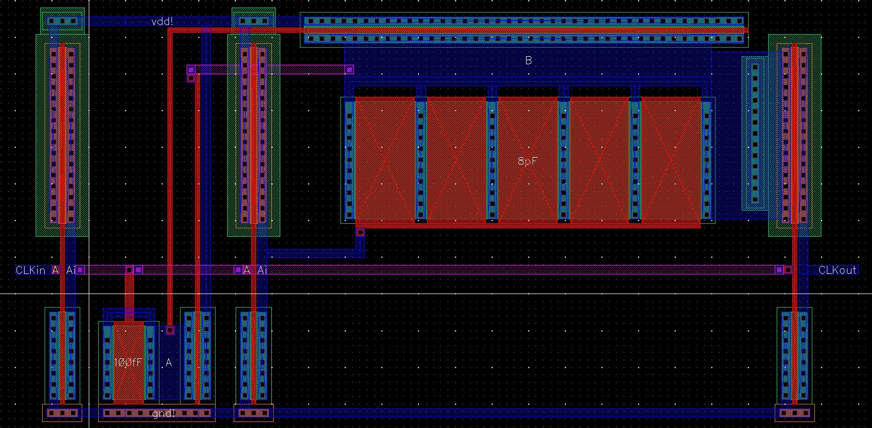
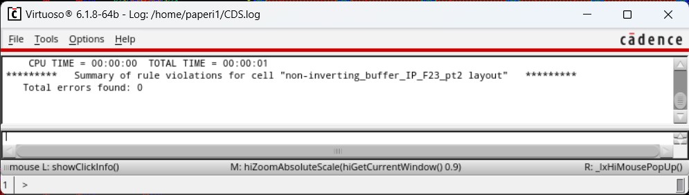
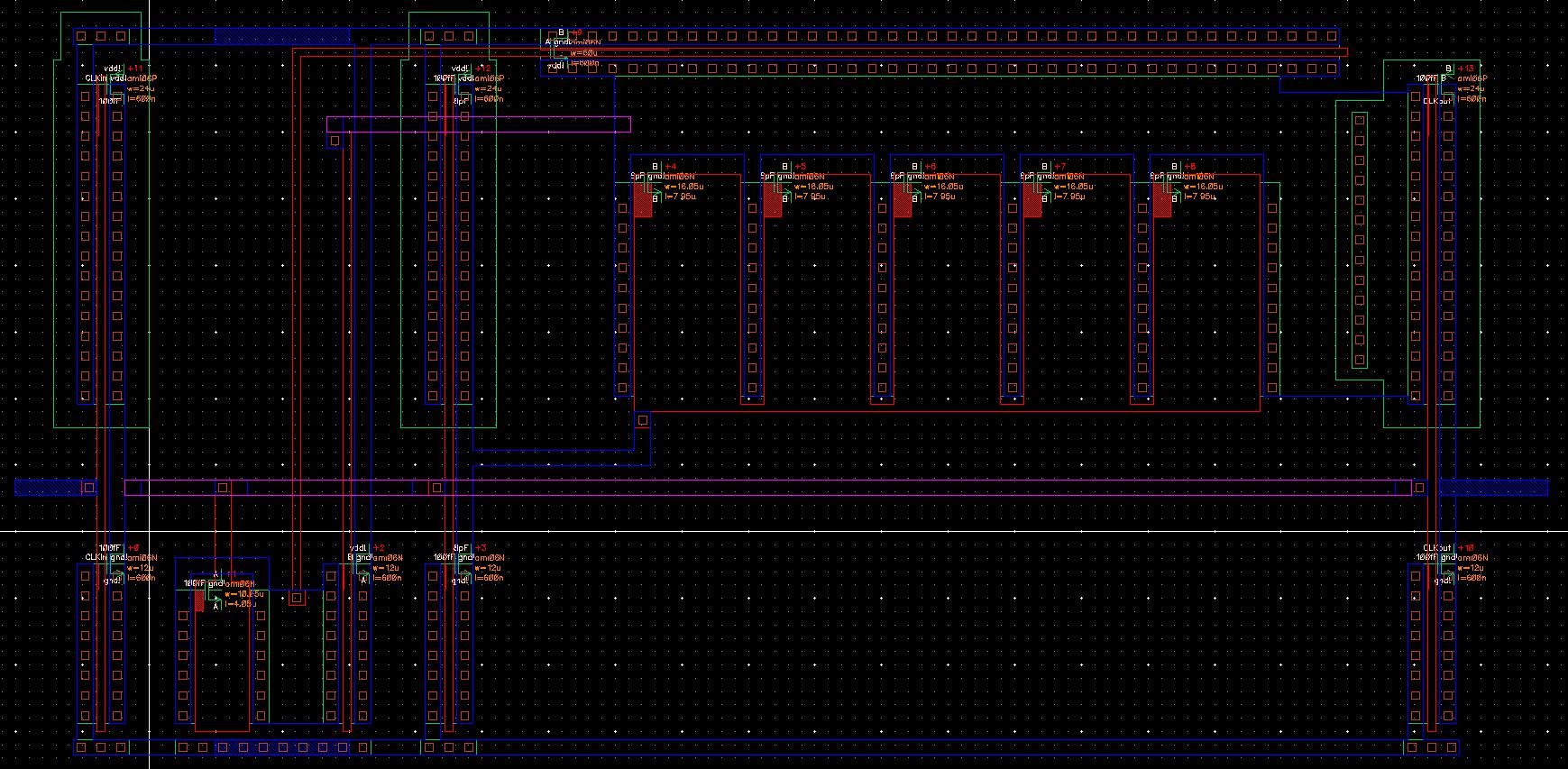
While this layout reported 0 errors through DRC, it initially failed the LVS verification. This was due to the layout automatically setting every ptap to the same net. I started building my layout to have some ptaps set to gnd! and others set to B, like in the schematic, but I would get errors regarding overlapping net names and extracting it would show that all the ptaps were set the same—either all gnd! or all B. This also caused more LVS errors as there were discrepencies between the amount of nets connected to A, B, and gnd! between the layout and schematic. So I adjusted my schematic to accurately represent what was occuring in the layout, making it so all NMOS devices had their bodies tied to ground, and that fixed all my errors.
This concludes the second half of the project, all work for my project can be found in two zip files. Work from the
first half can be found in project_lab_pt1_IP_F23 while the entire project can be found in project_lab_IP_F23.zip.
Return to EE421L Final Project Index