EE 421L Final Project
Project Task:
NOT A GROUP EFFORTPart 2: Layout and Documentation
Part 1 Preparation:
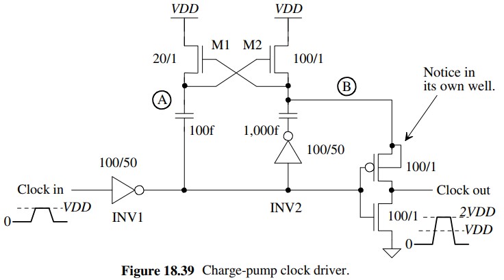
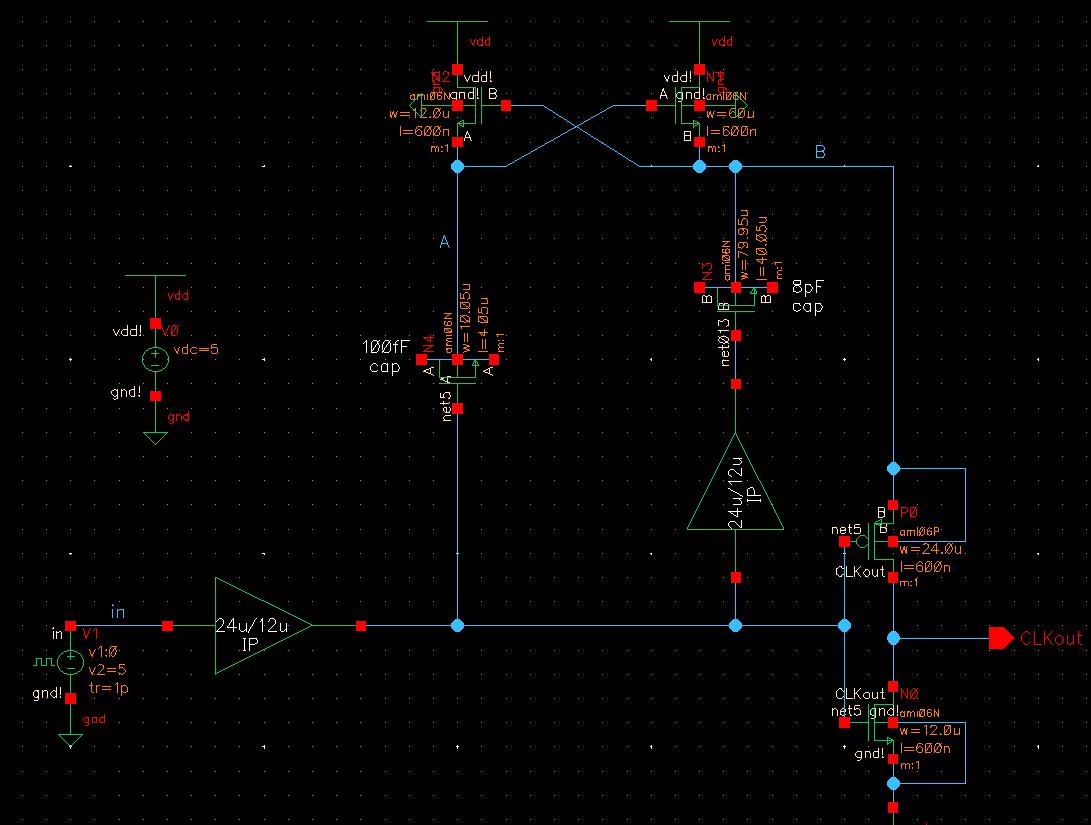
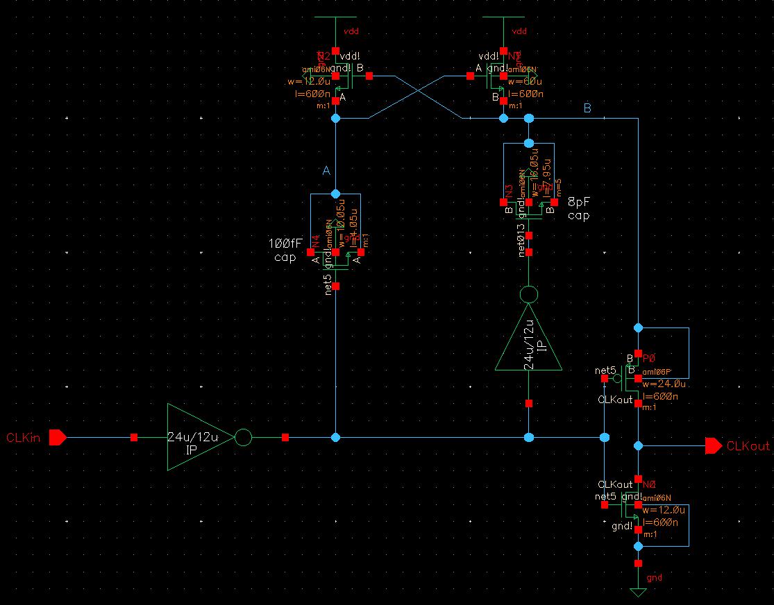
As preparation for this project, we were directed to Chapter 18 in our CMOS book, and told we could follow the charge-pump clock driver example found in Figure 18.39 (seen below) to design our project. This example is a non-inverting device that provides an output up to 2VDD, both of which tie in to the requirements of this project. Having the output reach up to 2VDD is essential for this project as we are allowed a VDD of 4.5V to 5.5V but can only get a logic 1 output if our output voltage is greater than 7V, even if we use the lowest VDD option (4.5V) the output voltage should be able to get to 9V exceeding the threshold for a logic 1 output.
Although this example is extremely useful, I could not just copy this figure as is. With the restrictions given, I had to calculate a decent size for each device within it and ensure that they all fit well together while maintaining the crucial 2VDD output.
Circuit Limitations:
Part 1 Procedures:
Input Inverter Creation and Simulations:
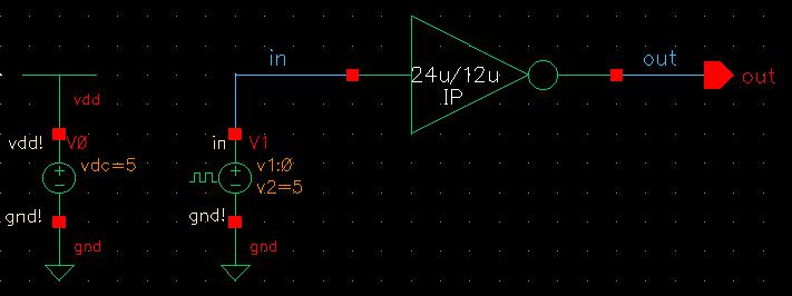
I started at the beginning of the circuit, specifically with INV1, to figure out a decent size that would maintain the limitation on the input capacitance.
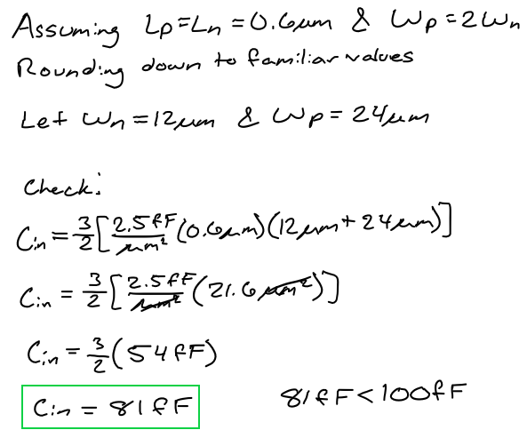
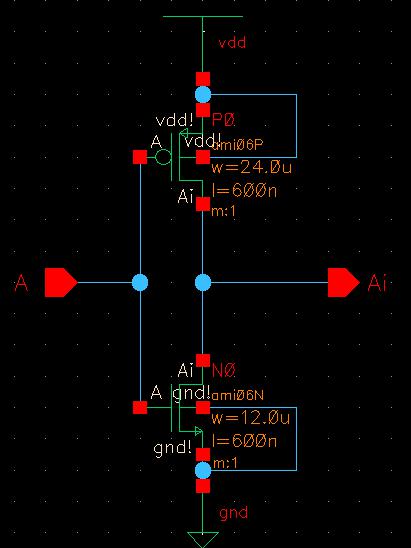
I started by assuming the inverter was using the minimun length (0.6um) then solving for the maximum width of the PMOS and NMOS devices. Solving for the maximum widths provided an input capacitance of 99.9fF which was way to close to the 100fF limit. As that input capacitance was obtained using the maximum widths, any smaller width would work better for this project, so I turned to some familiar values that I have used for my inverters all semester: Wp = 24um and Wn = 12um. I decided on the PMOS width being twice as large as the NMOS width as, not only were those the given values in class, but I felt that design would work better with the overall circuit rather than a smaller square. So, deciding on those values, I had to actually check to make sure they would keep the input capacitance below 100fF. And they did, the input capacitance with those values ended up being 81fF which is less than 100fF and gives plenty of room for error to work around.
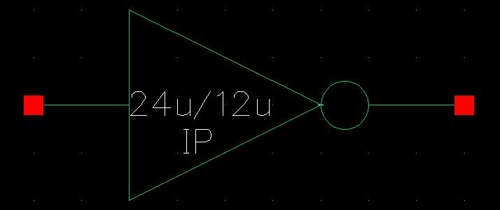
Now that I decided on the size, I quickly created the schematic and symbol for the inverter with Cadence.
To ensure the inverter was working properly, I conducted simulations with three possible VDD values: 4.5V, 5V, 5.5V.
From these simulations, I received the following switching point values:
| VDD | 4.5 V | 5.0 V | 5.5 V |
| Switching Point | 2.196 V | 2.468 V | 2.743 V |
A key thing to note is that the switching point changes depending on the provided VDD, however they are all within the expected range of ~2.5V and would not interfere with the input logic requirements for the project. I also used this same inverter for INV2.
Output Inverter Creation:
After completing the requirement for the input capacitance, I moved on to satisfying the output capacitance. For this final inverter—the inverter that produces the output—I needed to ensure that it would keep the entire device within the 4ns transition frame. Again, I was assuming the minimum length (0.6um) was being used for the inverter so I had to solve to the maximum widths of the NMOS and PMOS again, this time using the time delay formula. For this formula, I also needed a resistance value which I chose to be 1k. Other than this value being given to us in class (through this helpful note), I felt that 1k would be the easier value to deal with as it could quickly cancel out part of the load and remove a few orders of magnitudes.
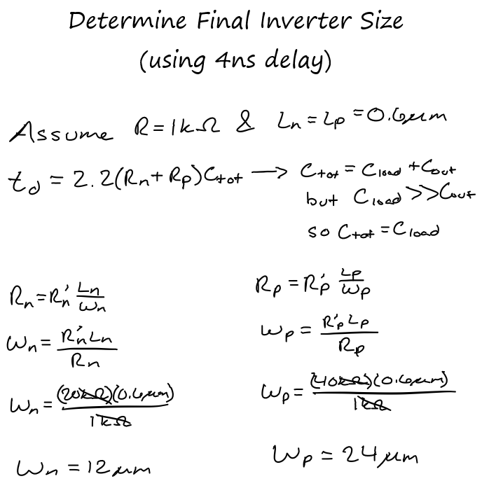
Here, I was able to obtain the inverter widths to be Wp = 24um and Wn = 12um which ended up being the same as the first inverter for this non-inverting buffer.
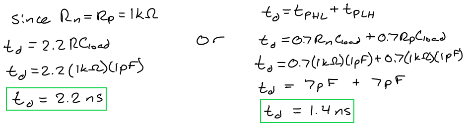
I also calculated my expected time delay at this time, using the 1k resistance value mentioned earlier. While the 2.2RC equation is the intended one to use, providing a delay of 2.2ns, I also wanted to see how much the delay could vary using the 0.7RC equation.
"Capacitor" Creations:
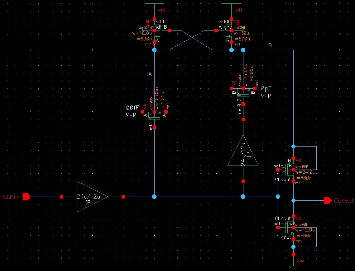
With all the inverters good to go, it's time to move up the circuit to the capacitors. Both capacitors will be created from NMOS devices in strong inversion rather than a poly-poly capacitor or an actual capacitor. The use of strong inversion is better than a poly-poly capacitor as seen by their resistance per square, with a poly-poly capacitor using 900aF/um^2 compared to the 2500aF/um^2 from an NMOS with the larger having better capacitance.The more important capacitor is the right one as that assists in obtaining the correct output so it must be larger. This capacitor also needs to be shared with the 1pF capacitive load that will be applied outside this non-inverting buffer, as they both feed directly into the output.
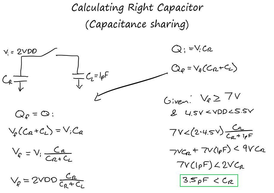
Since this capacitor needs to be larger than 3.5pF, I turned to digikey to help me select the best capacitance. I began my search at 5pF due to knowing the tolerance range could vary drastically depending on theh capacitance and I did not want to change picking a capacitor within the 4pF range and having it's tolerance dip below 3.5pF at any point. By starting at 5pF and looking upwards, I was ensuring the tolerance would not be an issue, allowing the NMOS to stay in strong inversion at all times.
| Capacitance range (pF) | Best Tolerance | Best Price |
| 5-5.9 | ±0.05pF for 5.6pF range: 5.55 - 5.65 | $0.00138 for 5.6pF |
| 6-6.9 | ±20% for 6.8pF range: 5.44 - 8.16 | $0.00138 for 6.8pF |
| 7-7.9 | ±0.05pF for 7pF range: 6.95 - 7.05 | $0.00175 for 7pF |
| 8-8.9 | +20%,-15% for 8pF range: 6.8 - 10 | $0.00126 for 8pF |
As seen on the table above, I found the best price to be $0.00126 for an 8pF capacitor with a decent tolerance range. Once I picked my capacitance, I had to figure out the best NMOS size for it.
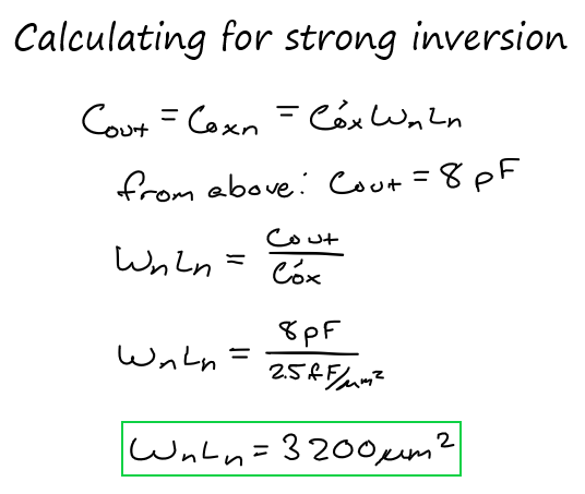
I ended up with WL=3200um^2 which could be split in two ways: W=80um, L=40um or W=64um, L=50um. So I made a chart comparing each option.
| W=80um L=40um | W=64um L=50um |
|
|
And the results of this led to me picking W=80um, L=40um for the NMOS.
Looking at the other capacitor, it's not as important since it does not impact the output so it could be much smaller. As it does not matter, I chose to use the capacitance it has in Figure 18.39, 100fF but I still needed to find the widths for the NMOS and PMOS.
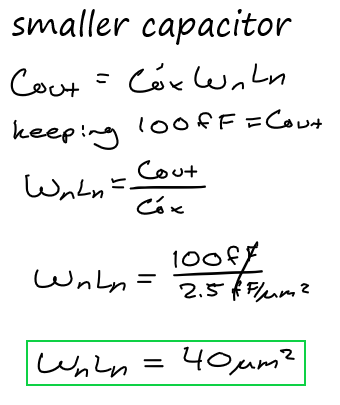
While this could also have multiple options—W=20um & L=2um, W=10um & L=4um, W=8um & L=5um—I chose to go with W=10um & L=4um as that had a closer W/L ratio (2.5) to the rest of my devices than the other options.
Last but not leasat, the top two NMOS devices. I chose to keep those the same as Figure 18.39 as it worked just fine when I tried it and I saw no reason to change something that worked.
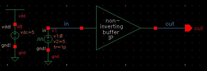
Complete Non-Inverting Buffer Schematic and Symbol:
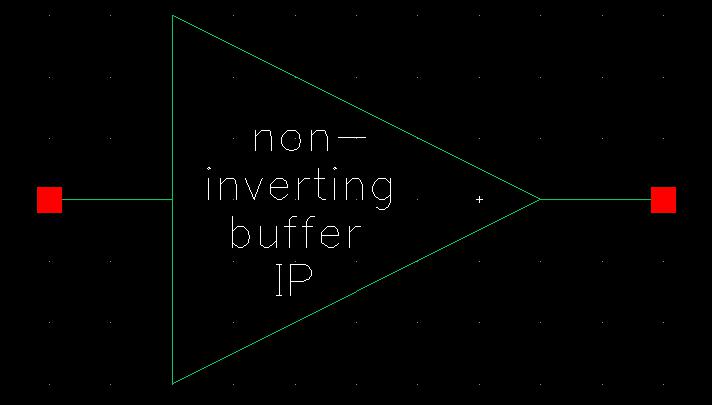
So my final circuit and symbol came out as the following.
Non-Inverting Buffer Simulations:
Now that the buffer is complete, I can begin testing it with simulations to ensure it works properly.
The first set of simulation tests is to see if net B actually becomes 2VDD as expected. The simulation is a simple input pulse from 0 to 5V and checks if B changes from VDD to 2VDD using three different VDD possibilities: 4.5V, 5V, and 5.5V.
| VDD | B low | B high | CLKout |
| 4.5 V | 4.2 V | 8.6 V | 8.6 V |
| 5.0 V | 4.75 V | 9.6 V | 9.6 V |
| 5.5 V | 5.3 V | 10.65 V | 10.6 V |
With each test, I noticed B actually starts at ~0.25V below the provided VDD but it does double the initial value, displaying that it works as intended. I believe the misalignment in VDD is due to some resistance between net B and the input lowering the voltage before it can reach B. I also noticed that it's only about a 5% error range, which matches the tolerance levels of the capacitor I picked, so that may be the cause as well.
The next set of simulations is testing the full non-inverting buffer with no load.
I started this set of testing changing the input voltage from 0 to 3V to make sure that the output is a logic 0 at or below 1V and a logic 1 at or above 3V.
![]()
I also tested input voltages at 2V and 2.5V to demonstrate that the output is unsteady during the switching point, hence why there is no logic 1 or 0 between 1V and 3V.
Then this last simulation for no node is showing the rising and falling times at the highest possible VDD (5.5V) since if the total delay is still within 4ns at the highest VDD then the lower VDDs will safely be within it.
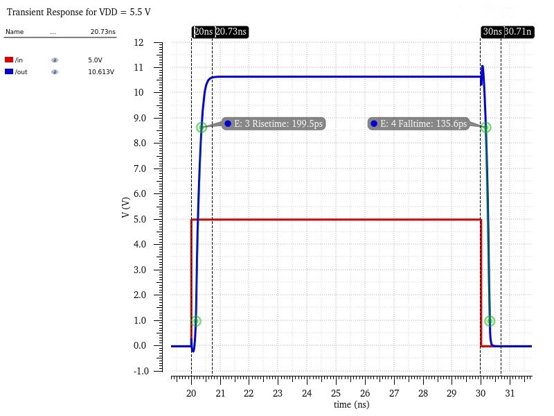
According to Cadence's rise/fall time calculations (which only account for 20%-80% of the edge) the total delay (199.5ps+135.6ps) is 0.3351ns which is well within the 4ns range. You can also see from my markers, which is closer to the true 100% edge, that the delay is ~0.7ns, which again is well within the 4ns limit.
Last but not least are the simulations for the full non-inverting buffer with a varying capacitive load that maxes out at 1pF.
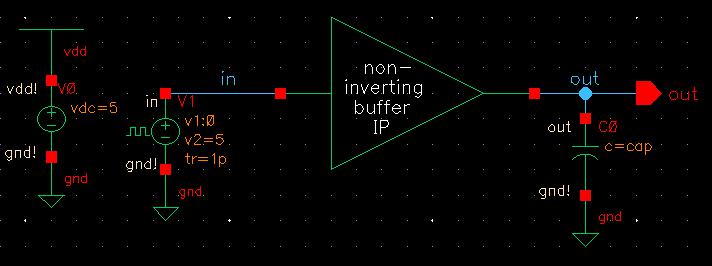
Now that a capacitor is involved, I created a parametric analysis that increases the capacitor from 0 to 1pF in 5 step (showing when the capacitor is at 0, 200fF, 400fF, 600fF, 800fF, and 1pF). However, I wanted to double check that the circuit still provides a logic 1 for an input of 3V or more and a logic 0 for inputs 1V or less.This graph demonstrates that the output logics are still intact once the load was added as there is an output of logic 1 with vin = 5V and an output of logic 0 with vin = 1V.
Knowing that the logic is still sound, I ran simultaions for the different VDDs, all with Vin = 5V, for when the capacitor is at 0, 200fF, 400fF, 600fF, 800fF, and 1pF. Below are all the rise and fall times, supplied by Candence (which is only showing the times from 20%-80% of the edge), for each load. The linked images only show the times for the 1pF and 0 loads as to not crowd the image and sinceany in-between capactors as they all fall between 0 and 1pF so if those are safely within the 4ns limit then all of them are.
| VDD | 0F | 200fF | 400fF | 600fF | 800fF | 1pF | |
| 4.5 V | rise time fall time total delay | 170.2ps 117.9ps 0.2881ns | 375.8ps 297.5ps 0.6733ns | 591.6ps 478.4ps 1.070ns | 793.4ps 639.2ps 1.4326ns | 990.4ps 796.1ps 1.7865ns | 1.183ns 953.5ps 2.1365ns |
| 5.0 V | rise time fall time total delay | 198.3ps 136.1ps 0.3344ns | 423.3ps 370.3ps 0.7936ns | 656.2ps 606.7ps 1.2629ns | 883.2ps 8244ps 1.7076ns | 1.098ns 1.038ns 2.136ns | 1.306ns 0.245ns 2.551ns |
| 5.5V | rise time fall time total delay | 206.4ps 136.2ps 0.3426ns | 416.5ps 360.5ps 0.7770ns | 640.8ps 586.4ps 1.2272ns | 861.2ps 798.4ps 1.6596ns | 1.071ns 1.008ns 2.079ns | 1.274ns 1.202ns 2.476ns |
Part 2 procedures:
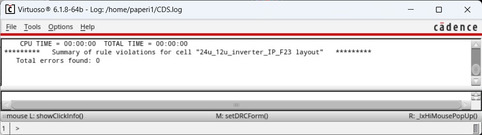
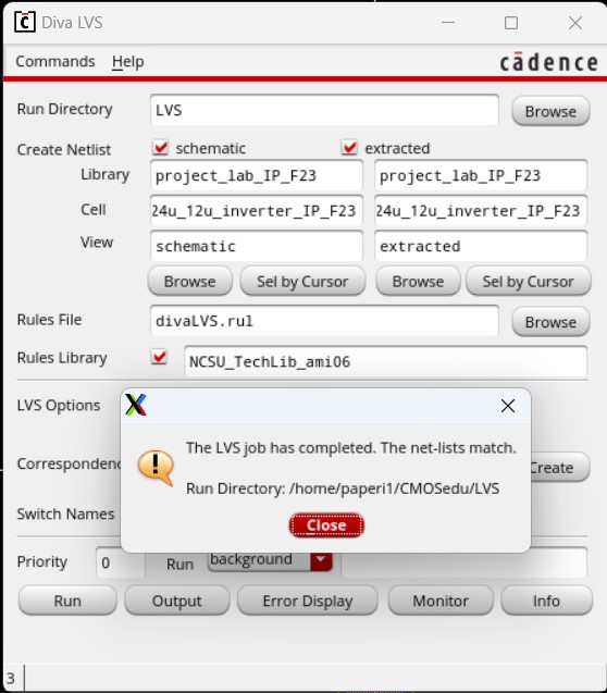
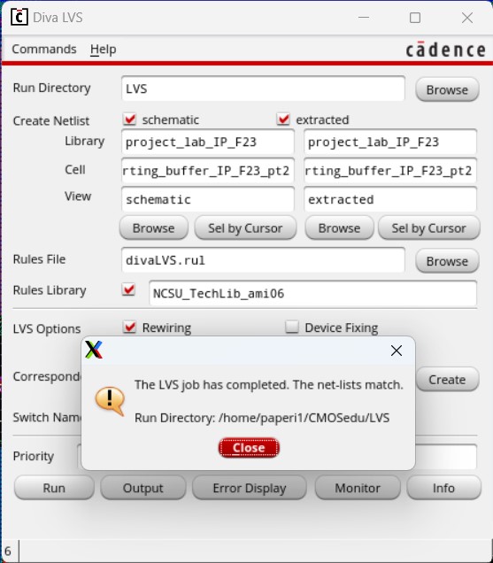
I started by laying out the 24u/12u inverter, to later be used in the non-inverting buffer layout, and verified it with DRC. Then I extracted the layout and ran LVS verification, looking for a match.
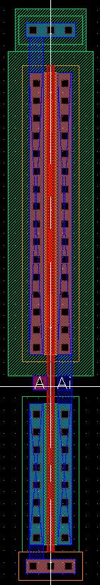 | 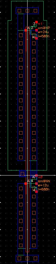 |
 |  |
Moving on to the complete layout, two of these inverter layouts were used as well as four separate NMOS layouts and another separately created inverter. There are four pins in this layout—input CLKin, output CLKout, inputoutput vdd! and inputoutput gnd!—as well as two labels (A and B) that correspond with the same labeled wires in the schematic.
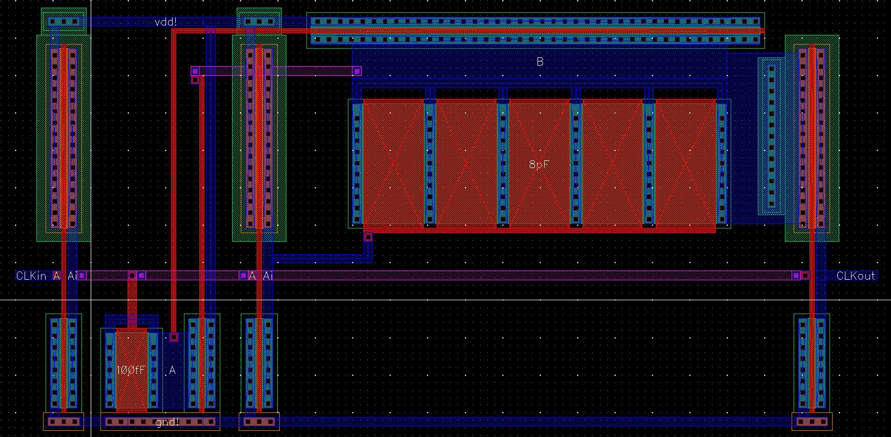
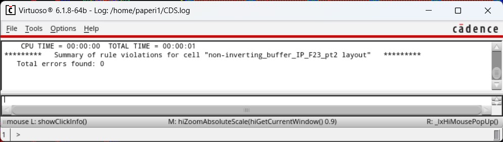
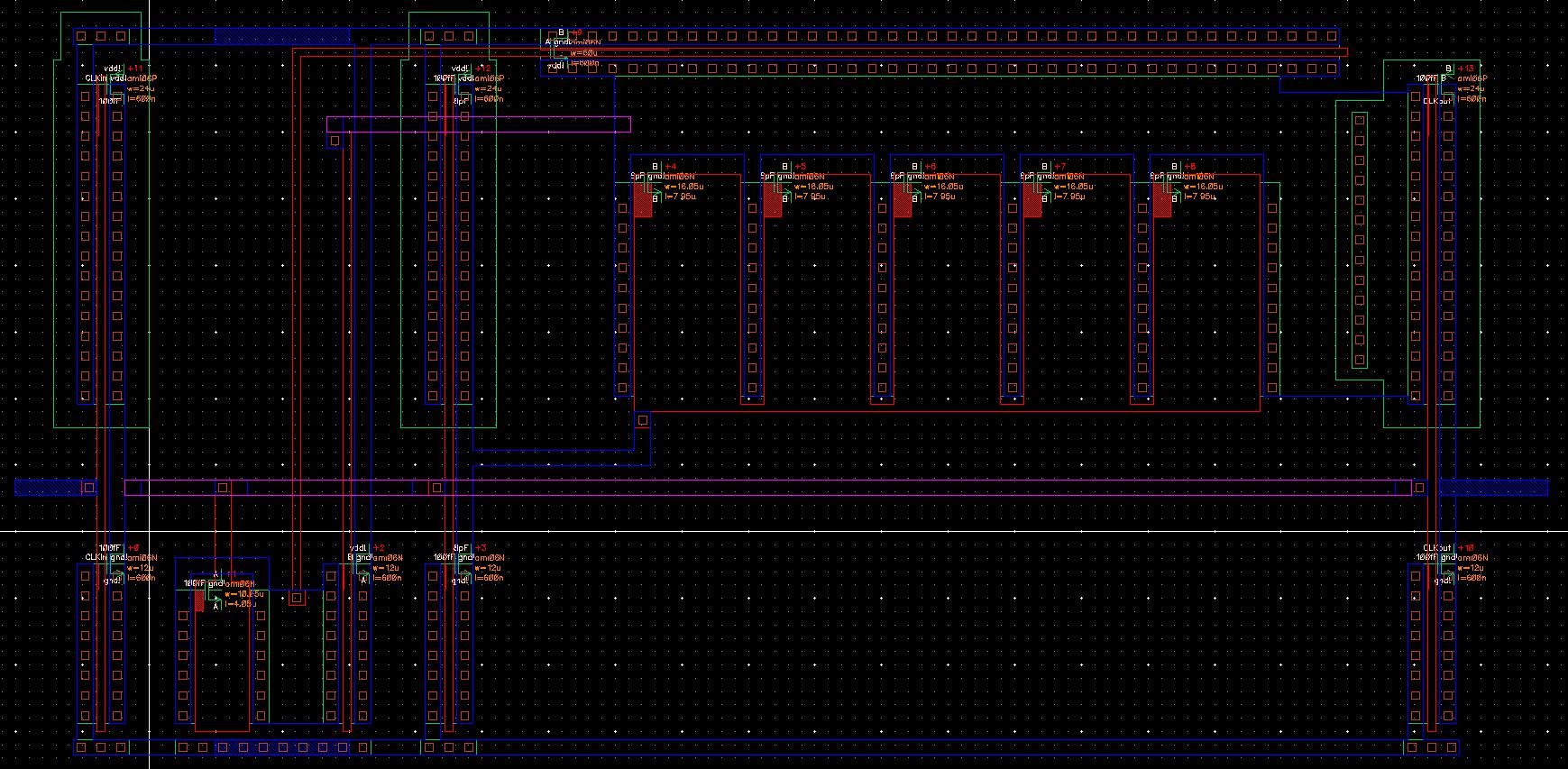
While this layout reported 0 errors through DRC, it initially failed the LVS verification. This was due to the layout automatically setting every ptap to the same net. I started building my layout to have some ptaps set to gnd! and others set to B, like in the schematic, but I would get errors regarding overlapping net names and extracting it would show that all the ptaps were set the same—either all gnd! or all B. This also caused more LVS errors as there were discrepencies between the amount of nets connected to A, B, and gnd! between the layout and schematic. So I adjusted my schematic to accurately represent what was occuring in the layout, making it so all NMOS devices had their bodies tied to ground, and that fixed all my errors.
This concludes the second half of the project, all work for my project can be found in two zip files. Work from the first half can be found in project_lab_pt1_IP_F23 while the entire project can be found in project_lab_IP_F23.zip.
Return to EE421L Final Project Index