Lab 6 - ECE 421L
Authored
by Benjamin Molina, molinb1@unlv.nevada.edu
10/24/2023
Prelab:
As
always the prelab involves backing up previous work from the other labs
which was done by saving it on my laptop and zipping it and storing it
in Google Drive.
The rest of the prelab involves us to go through Tutorial #4 and
understand the designs of logic gates using PMOS and NMOS transistors.
The main focus of the tutorial was making a NAND gate, which will be
shown below.
| LVS Before Changing LVS Rules | Changing LVS Rules | LVS After Rules change |
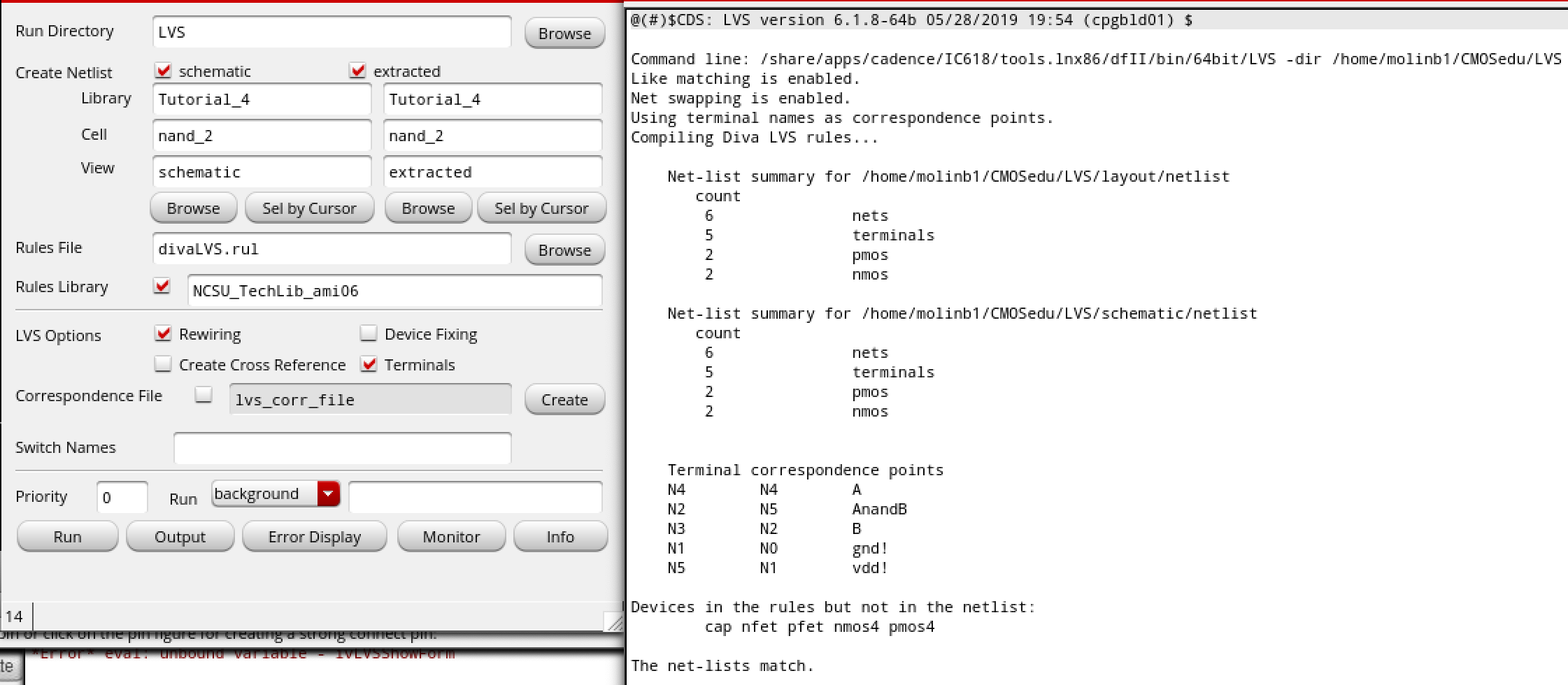 | 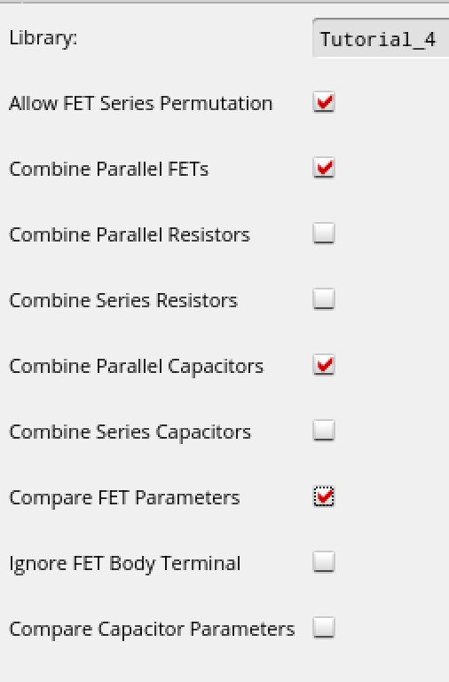 |  |
Tutorial
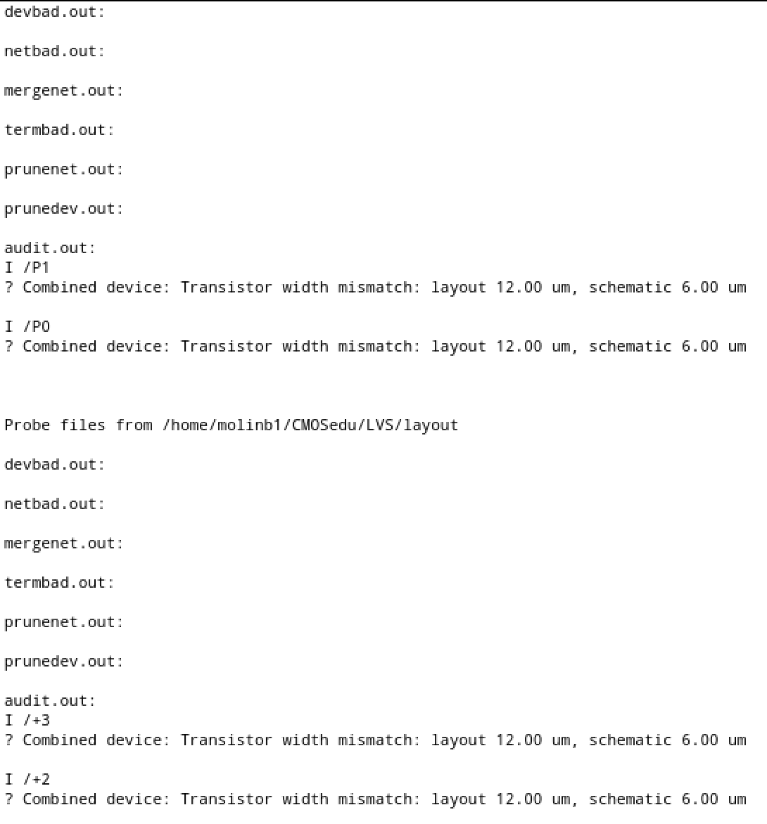
4 also emphasized that LVS normally ignores MOSFET sizes if they are
different so while the netlists may match, they may not be the same.
Changing the LVS rules to have it check when we have mismatched
parameters is a very helpful. For the rest of this lab this rule will
be checked to ensure accuracy.
Lab
description:
This
lab will have us design and layout a multitude of devices and
conponents that can be built with NMOS and PMOS transistors. The we
will build a NAND gate, a XOR gate, and finally design a Full Adder by
using a combo nation of the XOR and NAND gate.
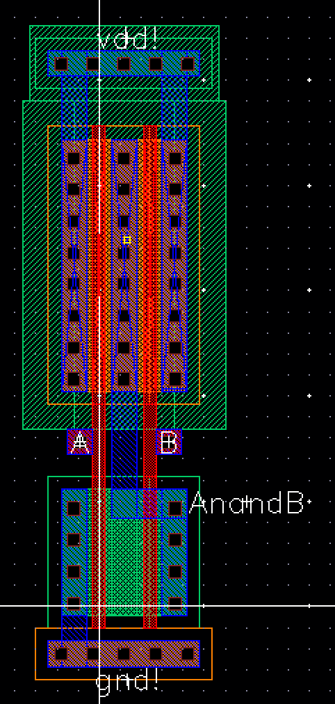
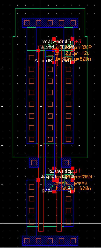
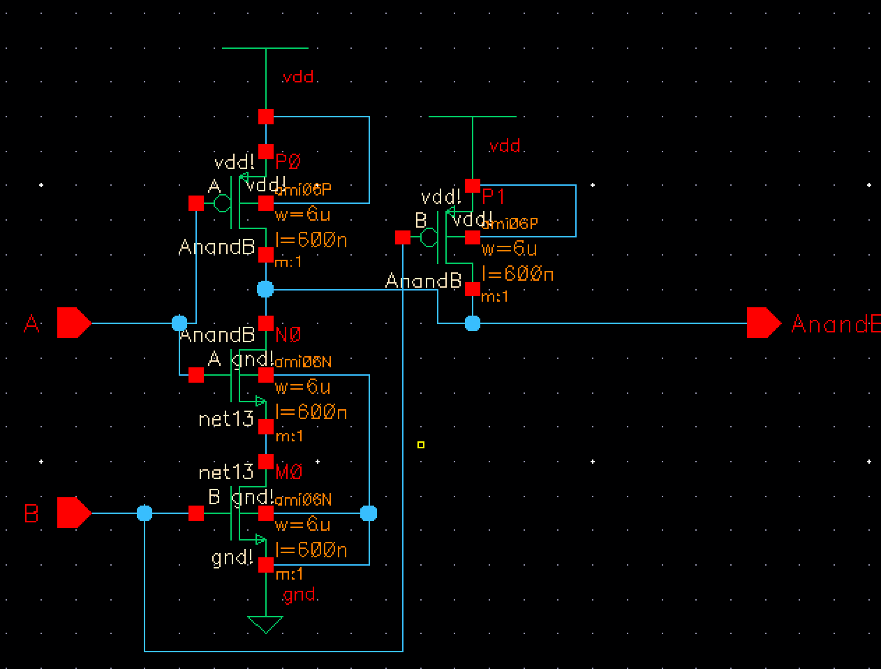
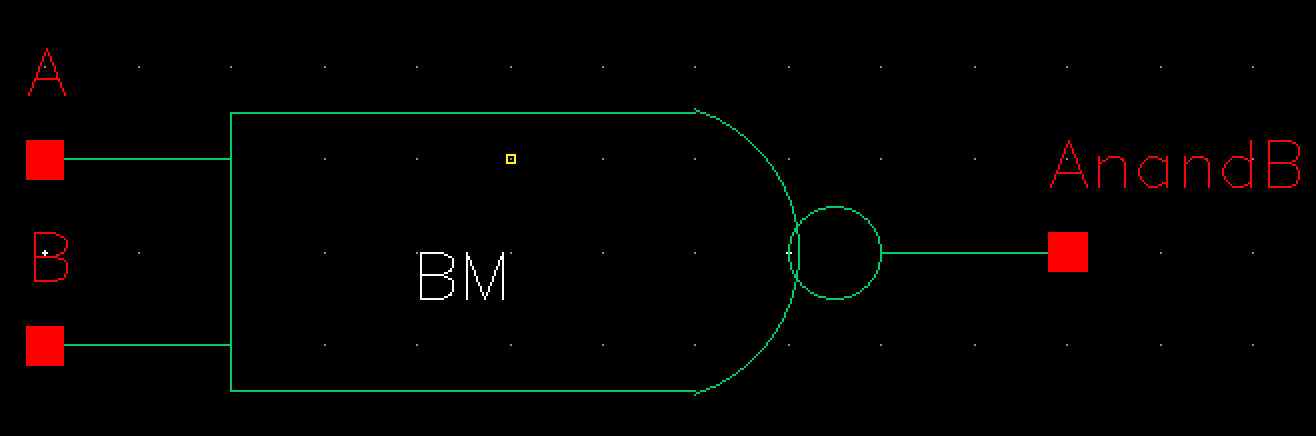
-NAND Gate Design:
First
we were asked to design a 2 input NAND gate schematic and layout. From
there we can make the symbol of a NAND gate and check to make sure the
netlists match for a 6u/.6u size.
| Schematic | Symbol |
 |  |
| Layout/DRC | Extracted |
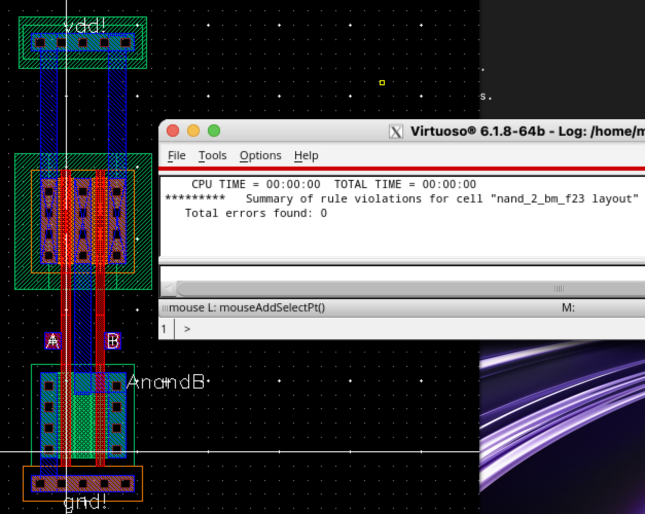 | 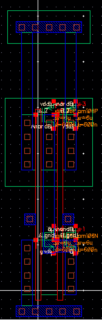 |
LVS Check: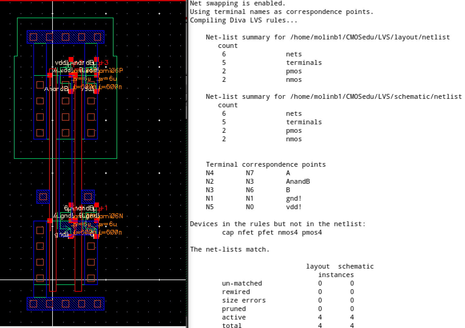 Schematic
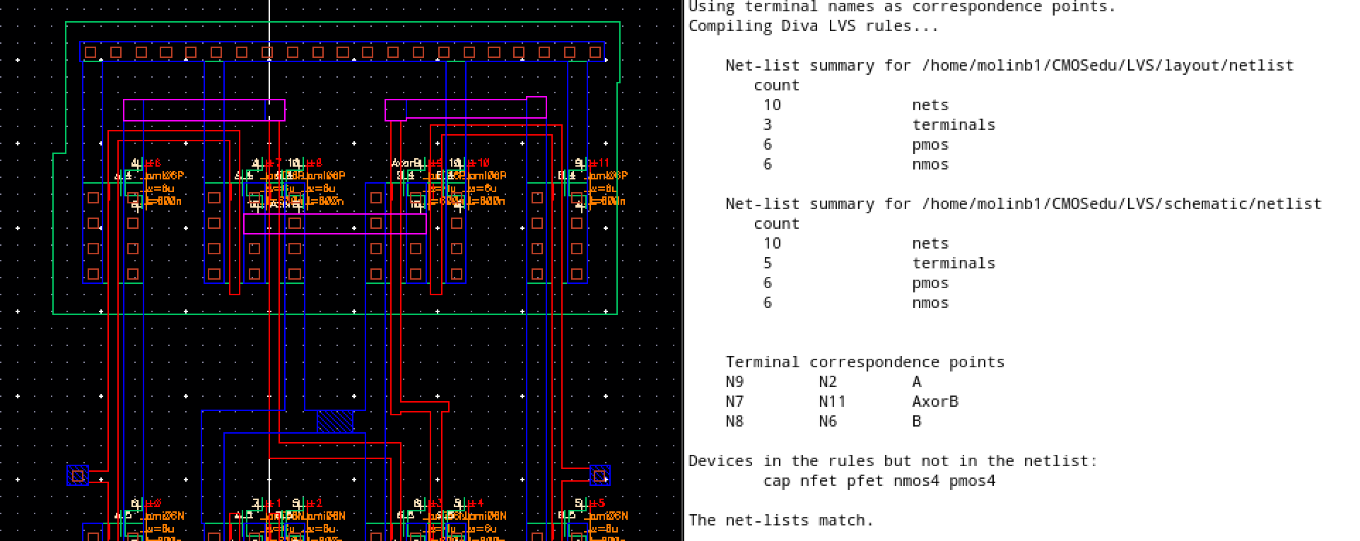
-XOR Gate Design:
Now
we wish to design a 6u/.6u XOR gate using a similar procedure and check
that the netlists will match for the extracted view and schematic.
Schematic
| Symbol |
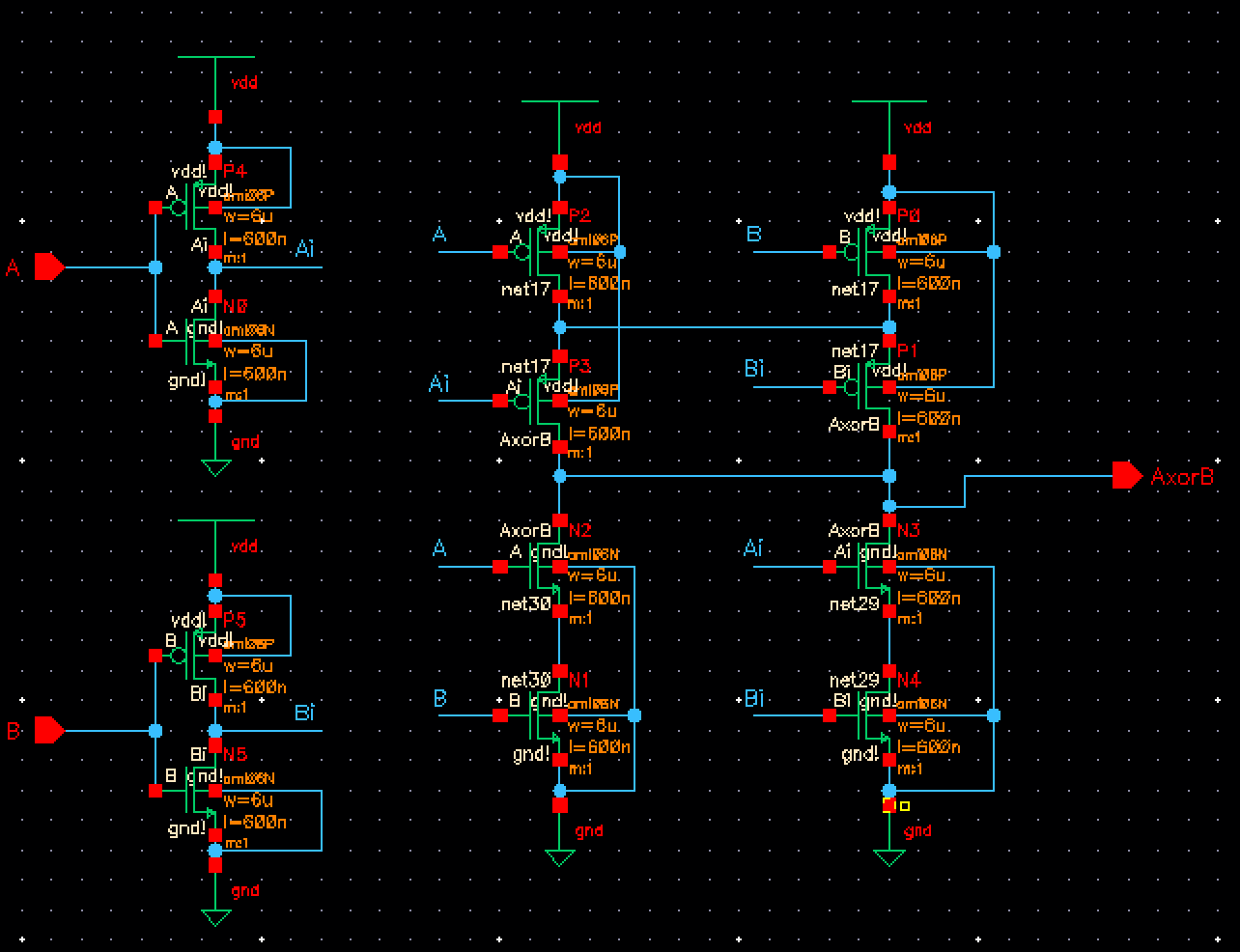 | 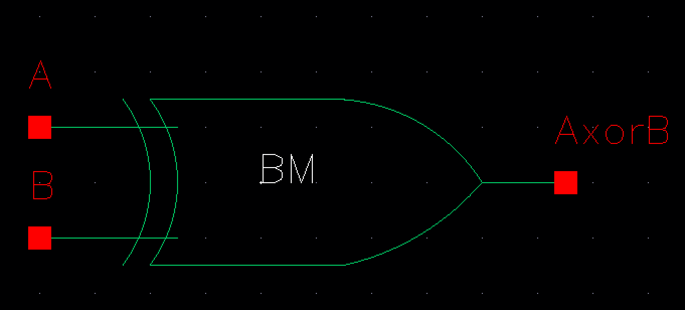 |
| Layout/DRC | Extracted |
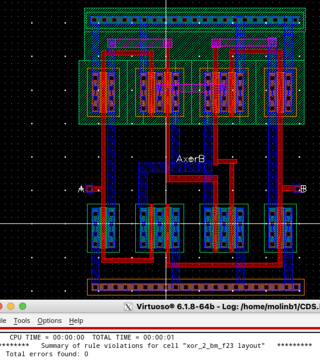 | 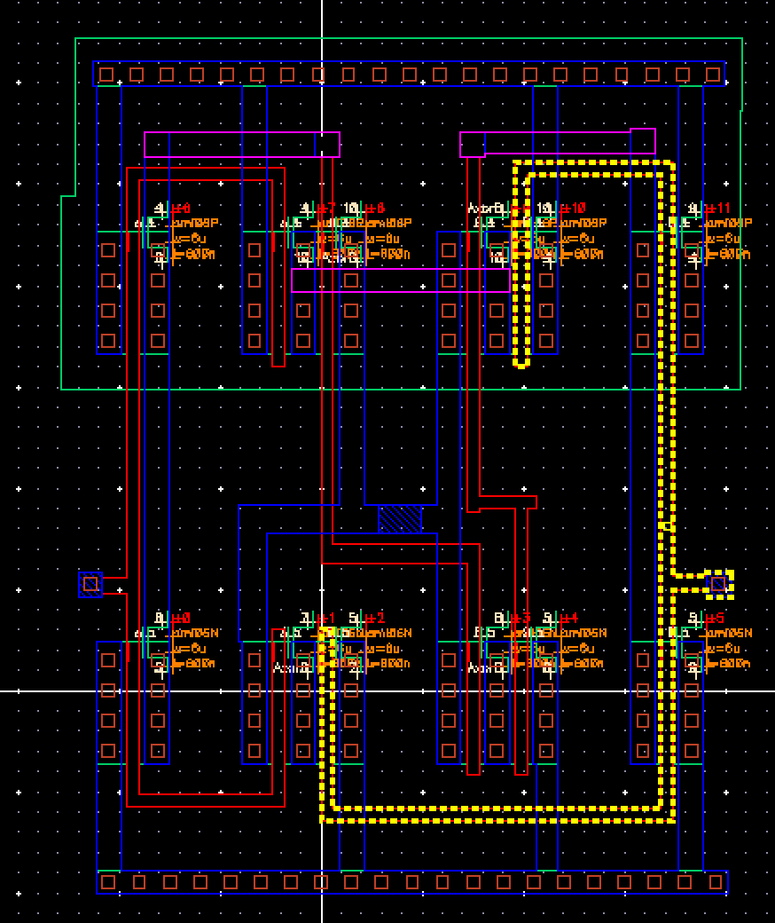 |
LVS Check:
Truth Tables:
Now we wish to prove that our logic gates can actually preform logic based on inputs given into it.
The basic truth table for all the devices we've designed so for goes as follows:
| A | B | Ai | NAND | XOR |
| 0 | 0 | 1 | 1 | 0 |
| 0 | 1 | 1 | 1 | 1 |
| 1 | 0 | 0 | 1 | 1 |
| 1 | 1 | 0 | 0 | 0 |
The simulation below handles all the logic gates in one plot.
| Schematic | Simulation |
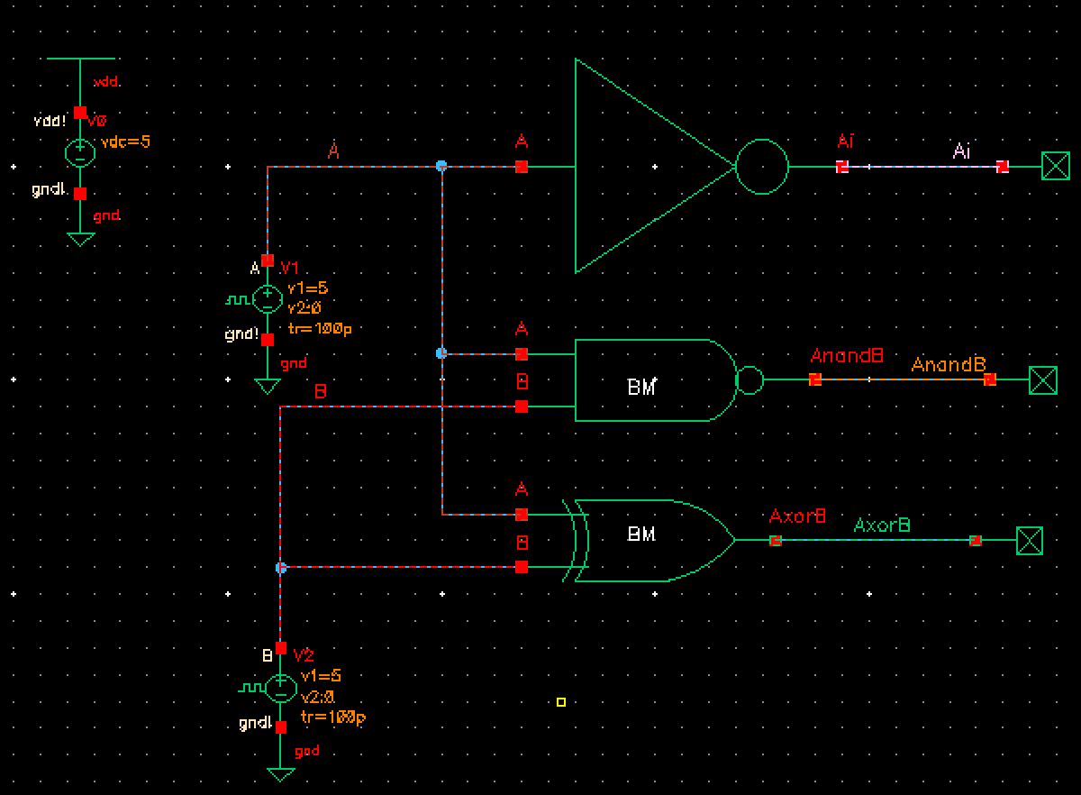 | 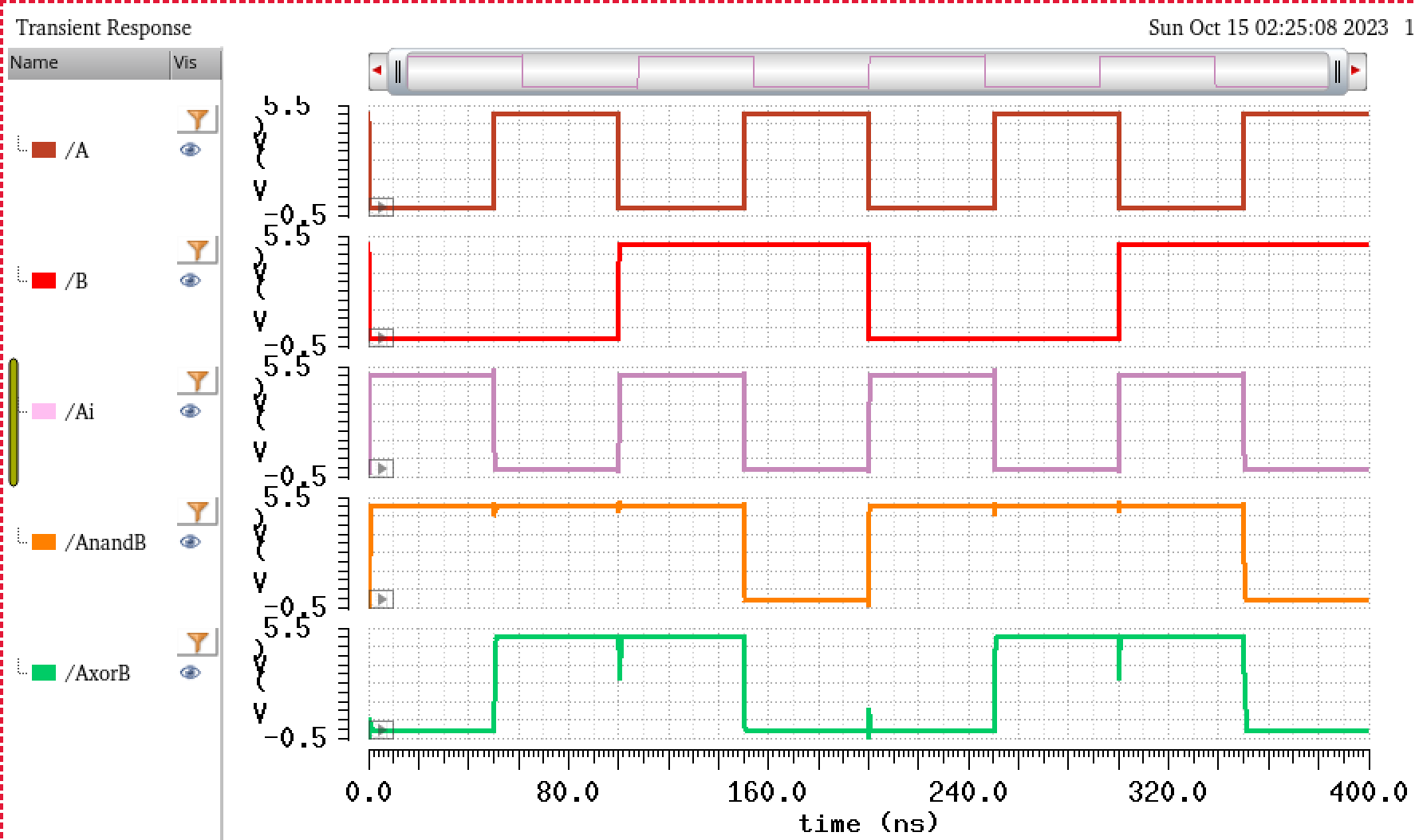 |
Based
on the simulation we can see that we indeed get the logic outputs that
match the truth table. Now we notice the random bumps in the outputs.
These result from the rise and fall times of the pulse that do not let
the device instantly change from one value to another.
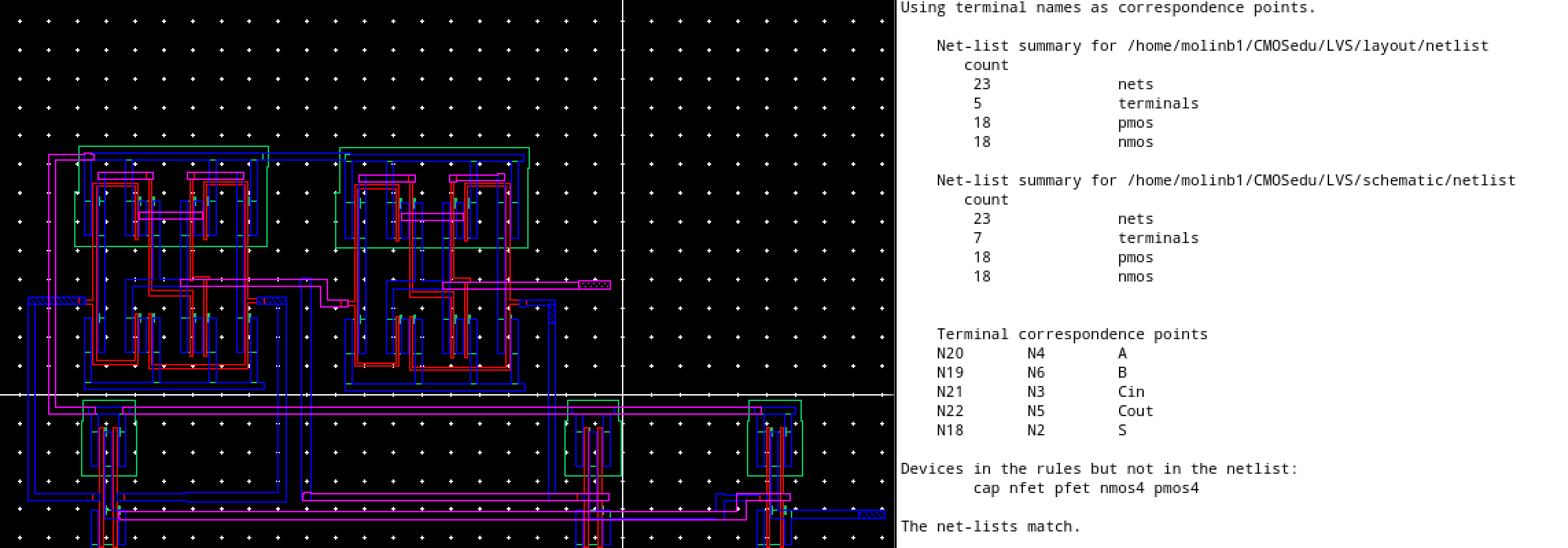
-Full Adder Design:
Now
we want to use both the NAND and XOR gate to design a Full Adder. Which
is able to add bits together and take in carry-in bits while having the
outputs S and Cout which is a carry-out bit.
| Schematic | Symbol |
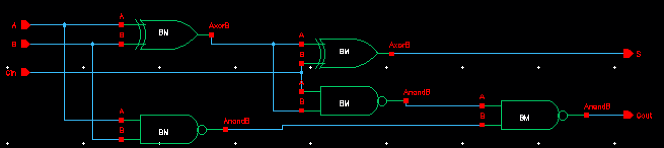 | 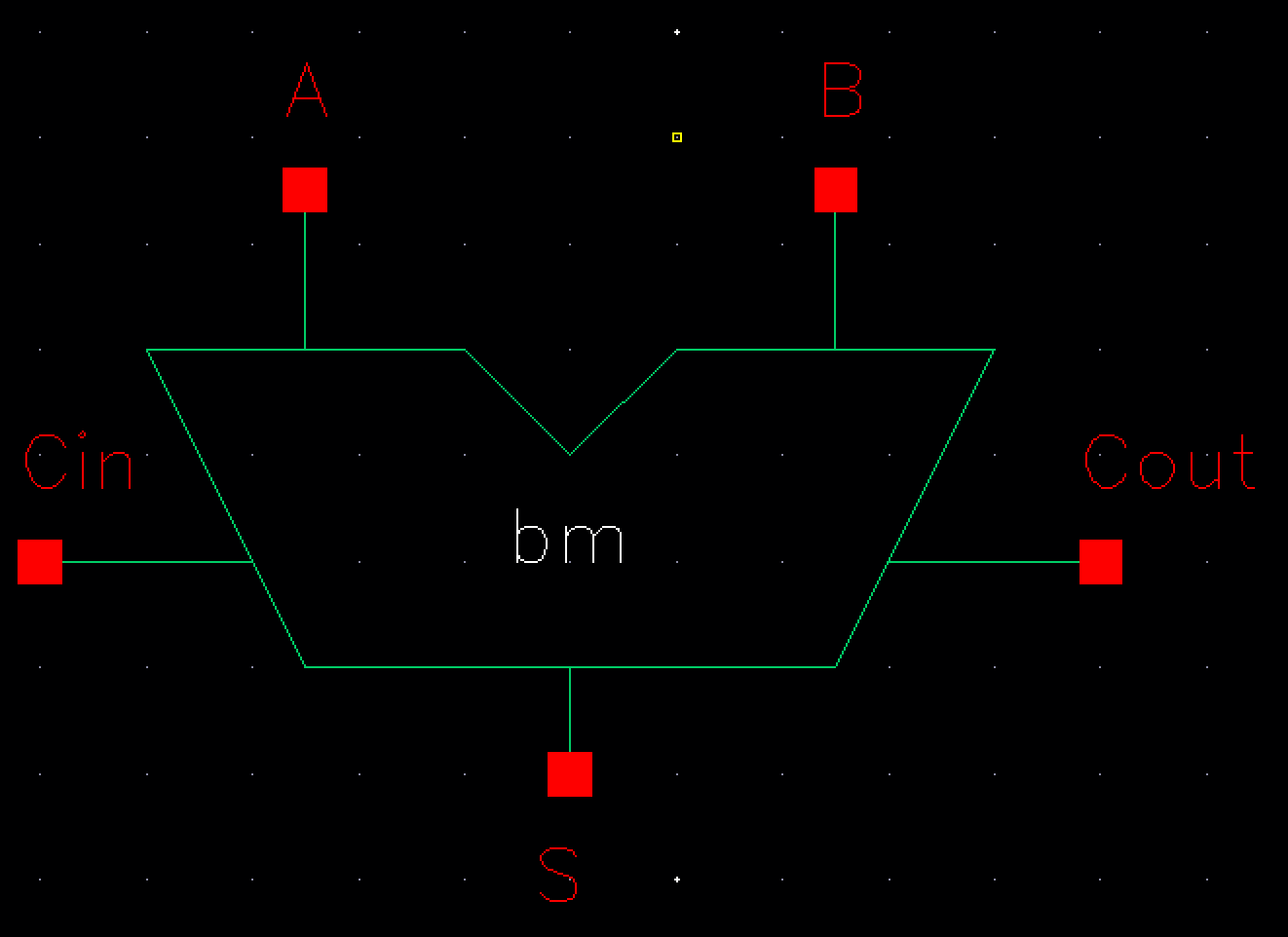 |
| Layout/DRC | Extracted |
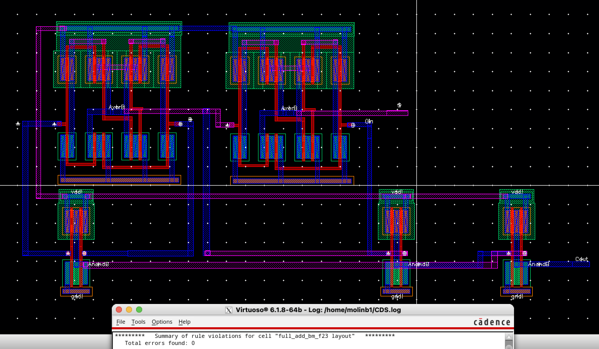 | 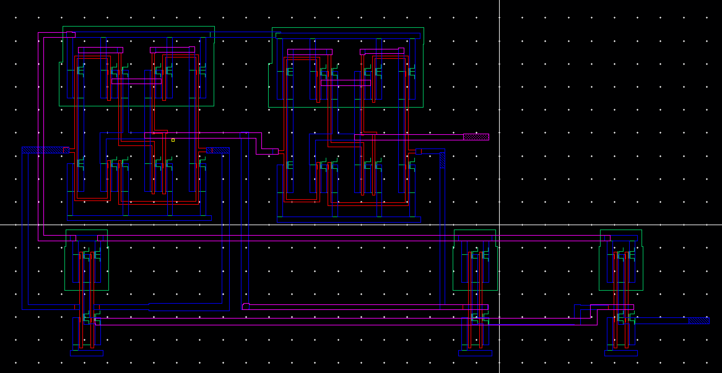 |
LVS Check:
Finally we want to simulate the Full Adder to prove it follows the truth table of a full adder as follows:
| A | B | Cin | S | Cout |
| 0 | 0 | 0 | 0 | 0 |
| 0 | 0 | 1 | 1 | 0 |
| 0 | 1 | 0 | 1 | 0 |
| 0 | 1 | 1 | 0 | 1 |
| 1 | 0 | 0 | 1 | 0 |
| 1 | 0 | 1 | 0 | 1 |
| 1 | 1 | 0 | 0 | 1 |
| 1 | 1 | 1 | 1 | 1 |
And from the follow simulation we can indeed see that they do match.
| Schematic | Simulation |
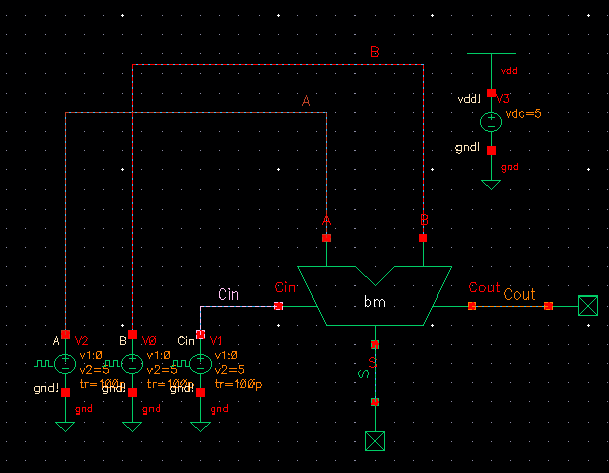 | 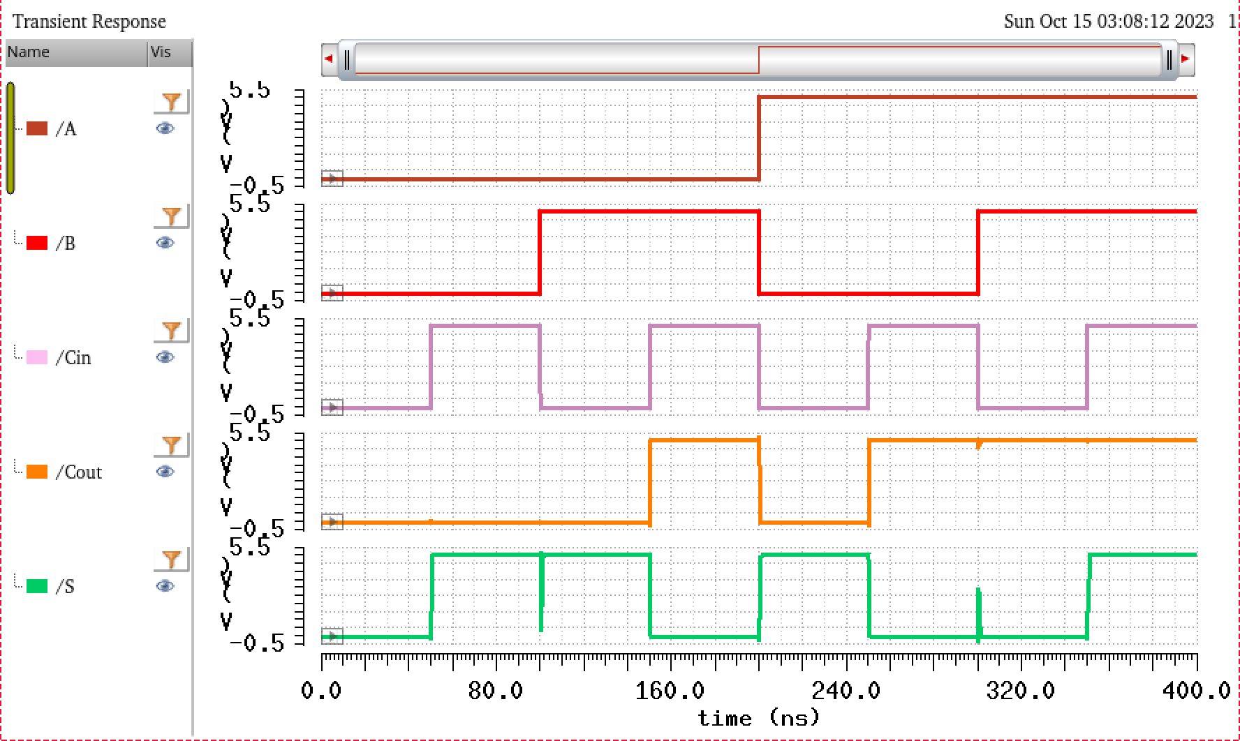 |
--------------------------------------------------------------------------------------------------------------------------------------------------------------------------------------------------------------------------------
As always work has been backed up and saved.

The zipped file containing the work done is here lab6.zip
Return to EE 421L