Lab 4 - ECE 421L
Authored
by Martin Mercado mercam13@unlv.nevada.edu,
09/26/2023
IV characteristics and layout of NMOS and PMOS devices in ON's C5 process
Pre-Lab:
- Back-up all of my from the lab and the course.

- Read through this lab before starting it.
- Go through Tutorial 2 seen here.
- In
the simulations in this lab the body of all NMOS devices (the
substrate) should be at ground (gnd!) and the body of all PMOS devices
(the n-well) should be at a vdd! of 5V.
For
Tutorial 2, I'm going to be laying out and simulating the operation of
NMOS and PMOS transistors using the C5 process form Tutorial 1.
First, I made a new library for Tutorial 2.

Now, the Tutorial will instruct me to make an NMOS schematic.
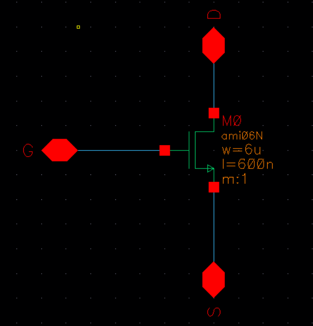
Then, I will create a symbol for the schematic.
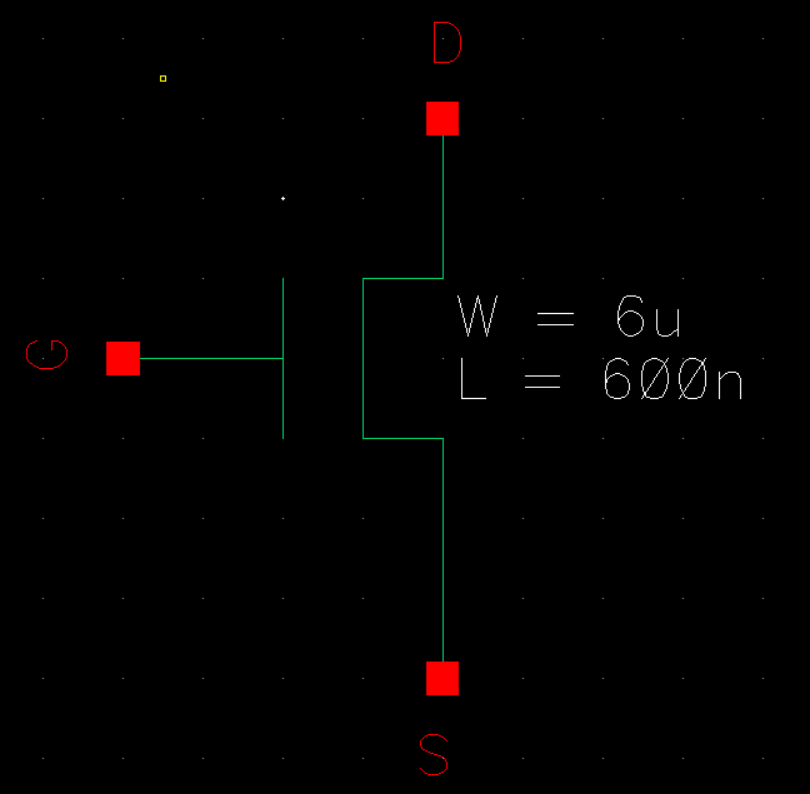
Using the symbol, I will make a new schematic.
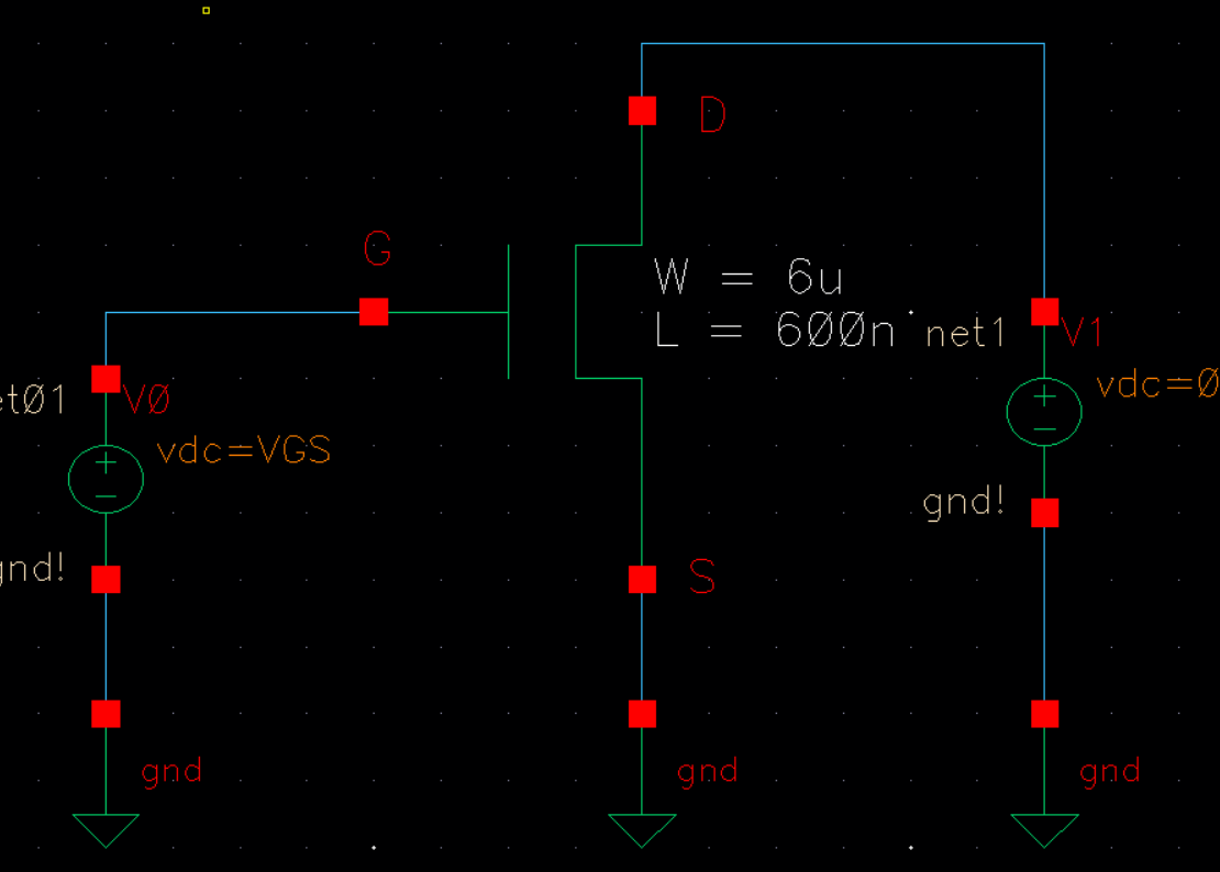
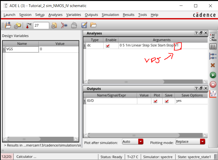
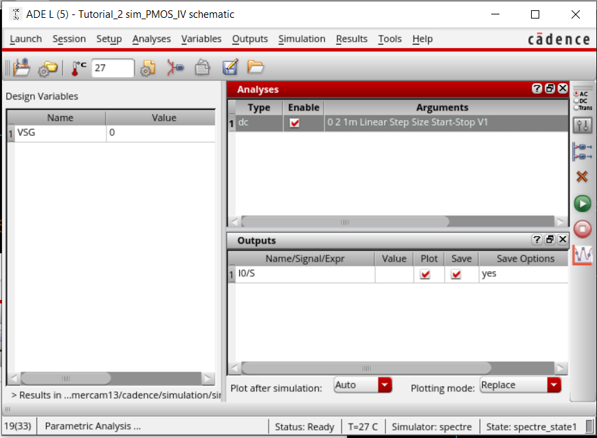
I will now simulate the schematic using parametric analysis.
I will now create a layout of the NMOS.
DRC and Extract.
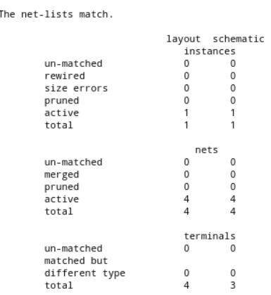
LVS will fail due to not have a 4-terminal transistor in the schematics.
Need to change schematic and LVS again.
Now we simulate the extracted layout.
Now repeat for PMOS.
Create the schematic then check and save.

Create a symbol.
Create a layout, then DRC and extract and LVS.
Next, I will simulate the PMOS.

Now I will simulate the extracted layout.
____________________________________________________________________________________________________________________________________
Lab:
Generate 4 schematics and simulations (see the examples in the Ch6_IC61 library, but note that for the PMOS body should be at vdd! instead of gnd!)
- A schematic for simulating ID
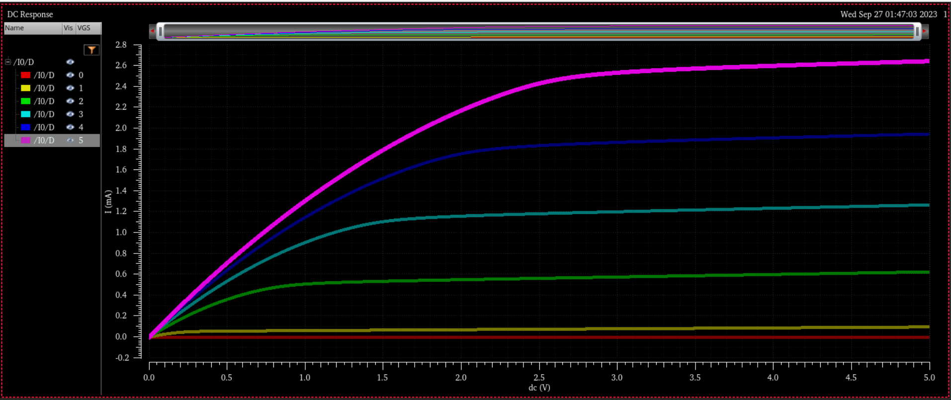
v. VDS of an NMOS device for VGS varying from 0 to 5 V in 1 V steps
while VDS varies from 0 to 5 V in 1 mV steps. Use a 6u/600n
width-to-length ratio.
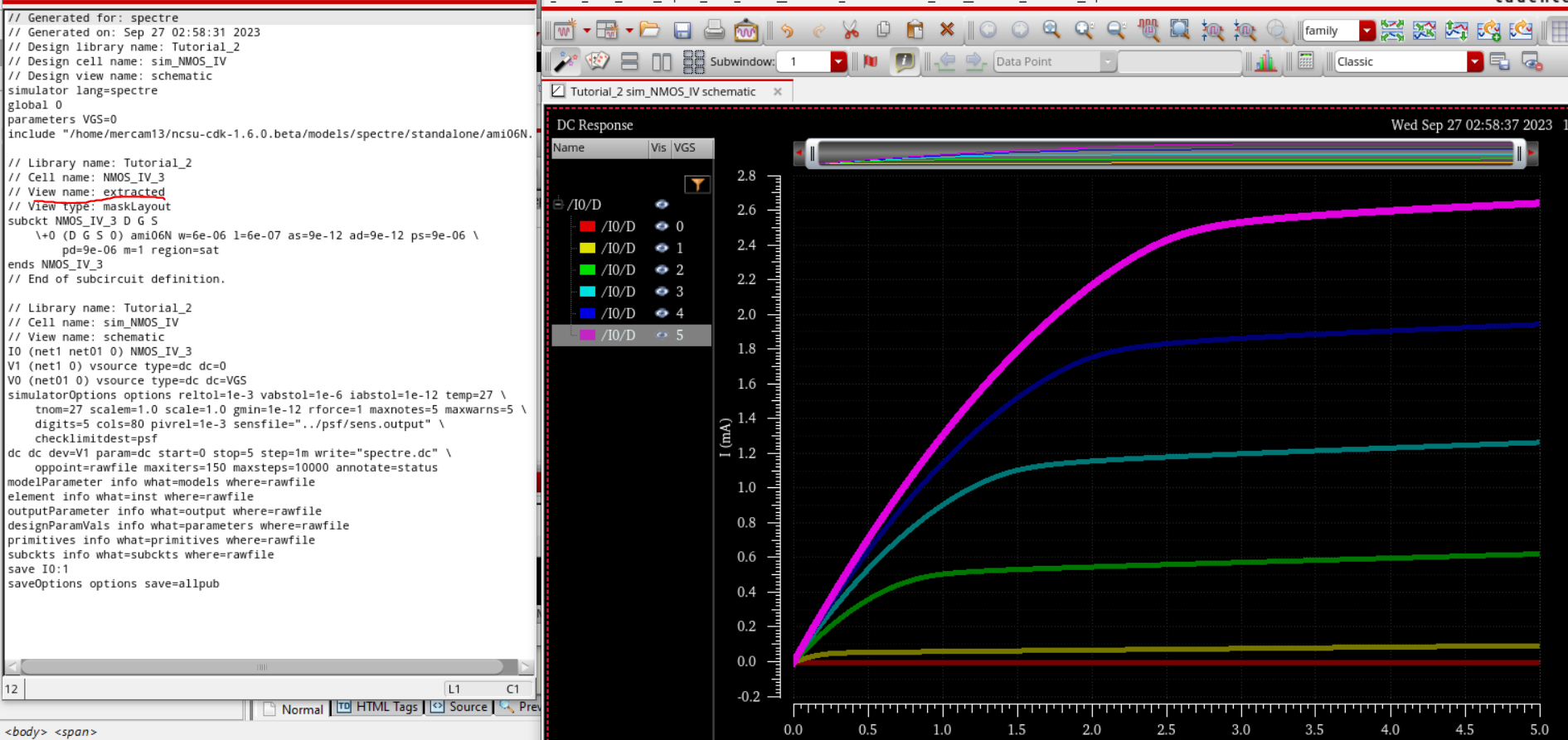
I will be using the schematic used made in the pre-lab to simulate.

As VGS increases, Id increases with respect to VDS.
- A
schematic for simulating ID v. VGS of an NMOS device for VDS = 100 mV
where VGS varies from 0 to 2 V in 1 mV steps. Again use a 6u/600n
width-to-length ratio.
Using the same schematic, I modify the values of VDS to 100mv. Then simulate where VGS varies from 0 to 2V in 1mV steps.
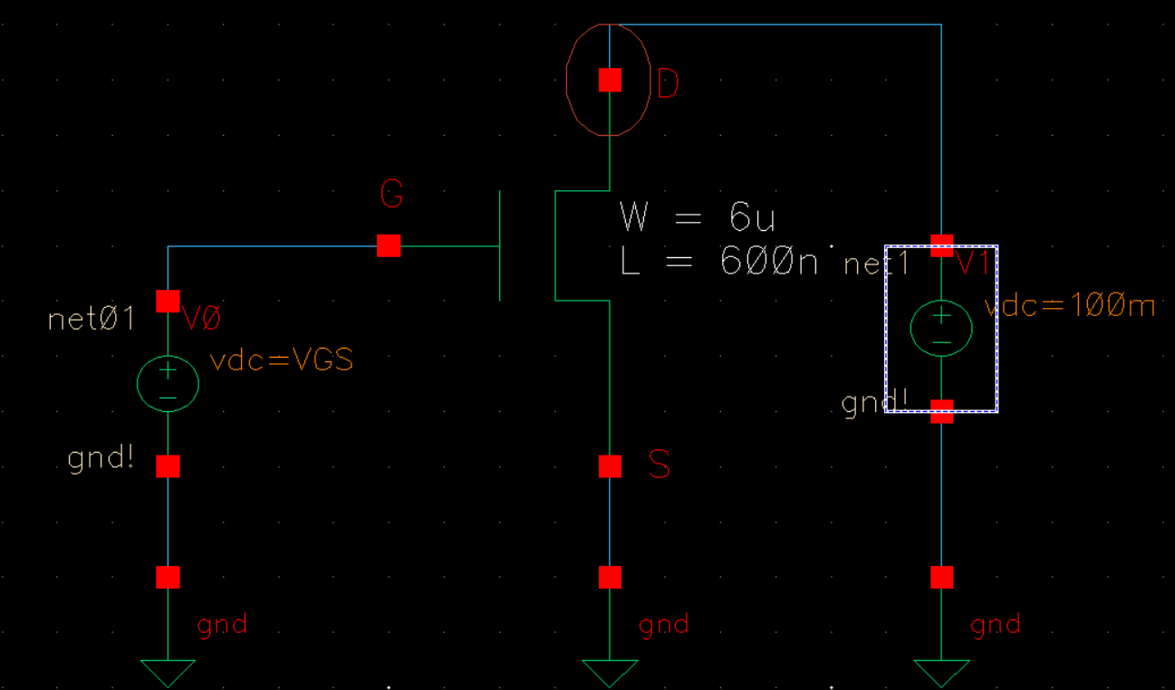
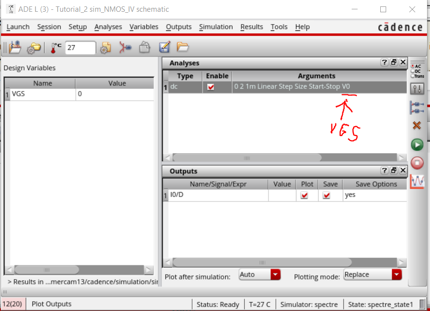
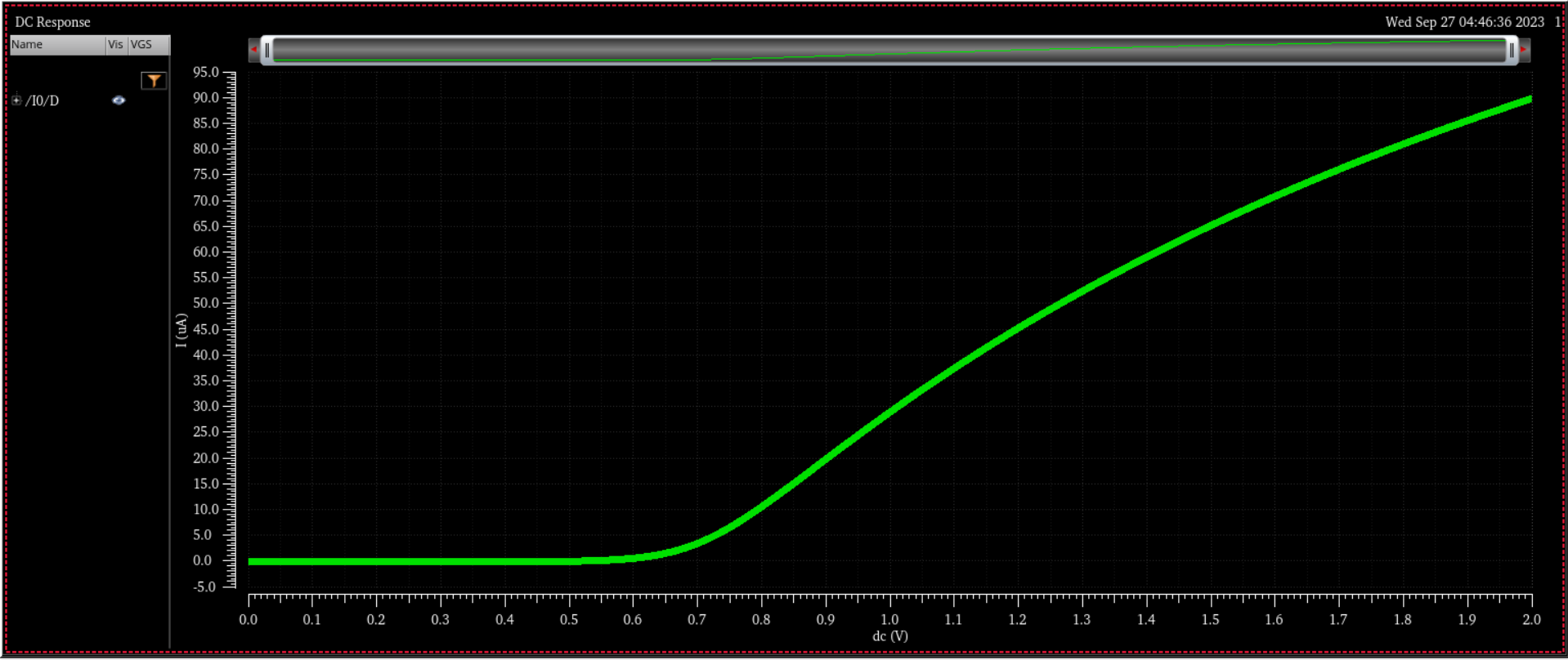
With an increasing VGS, Id increases too.
- A
schematic for simulating ID v. VSD (note VSD not VDS) of a PMOS device
for VSG (not VGS) varying from 0 to 5 V in 1 V steps while VSD varies
from 0 to 5 V in 1 mV steps. Use a 12u/600n width-to-length ratio.
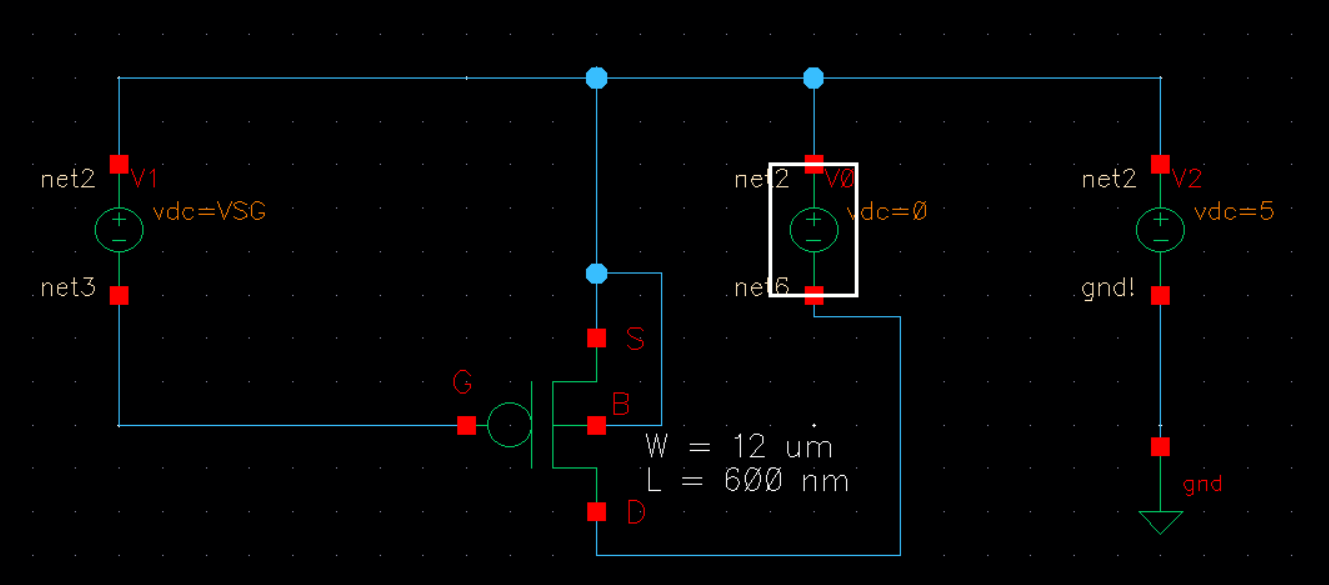
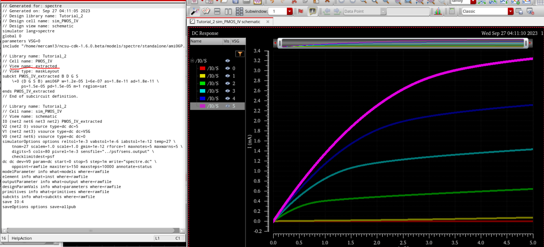
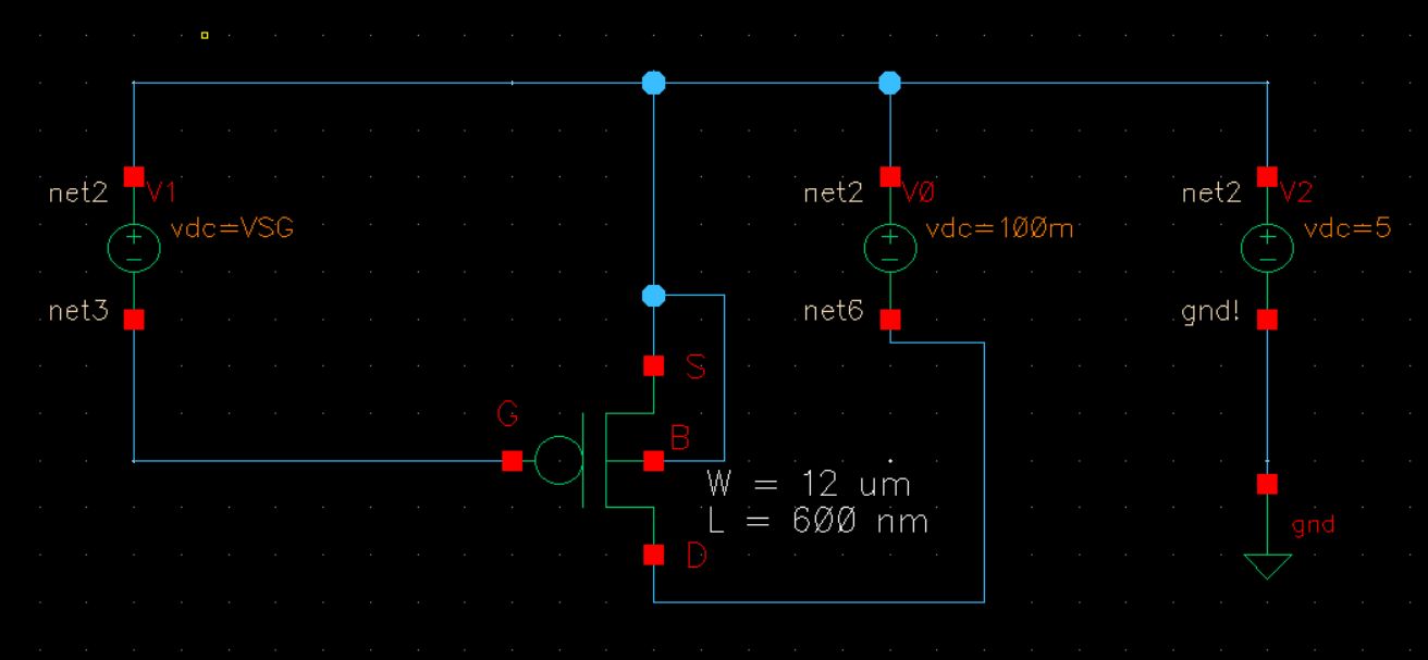
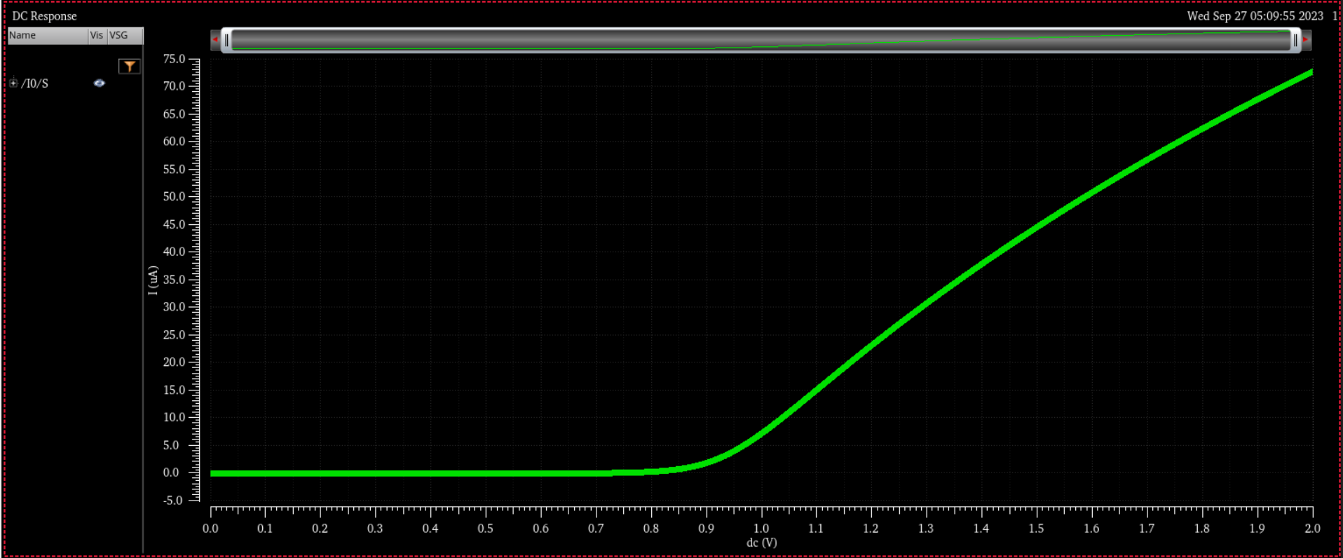
Using
the PMOS schematic created in the pre-lab, I will be simulating Id v.
VSD where VSG varies from 0 to 5V in 1V steps while VSD varies from 0
to 5V in 1mV steps.

As VSG increases, Id increases with respect to VSD.
- A
schematic for simulating ID v. VSG of a PMOS device for VSD = 100 mV
where VSG varies from 0 to 2 V in 1 mV steps. Again, use a 12u/600n
width-to-length ratio.
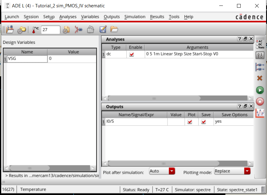
Modifying the PMOS schematic, I will simulate ID v. VSG for VSD=100mv and VSG varies from 0 to 2V in 1mV steps.

As VGS increases, Id increases with respect to VGS.
Note: The threshold voltage is higher because of the electrons being half as mobile as NMOS.
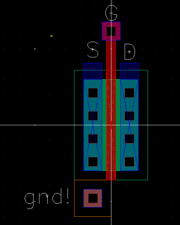
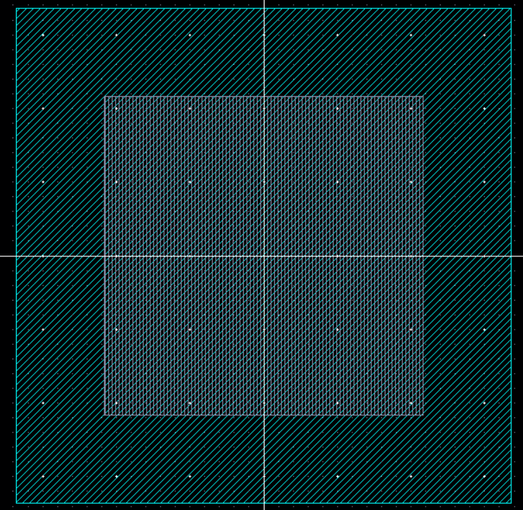
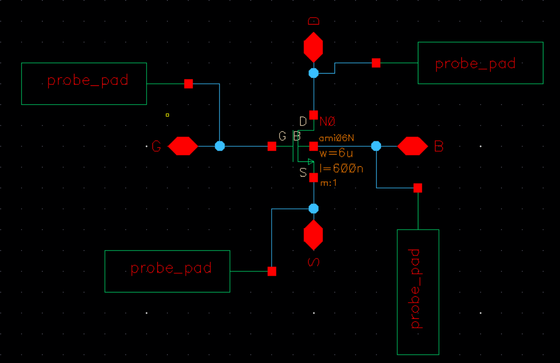
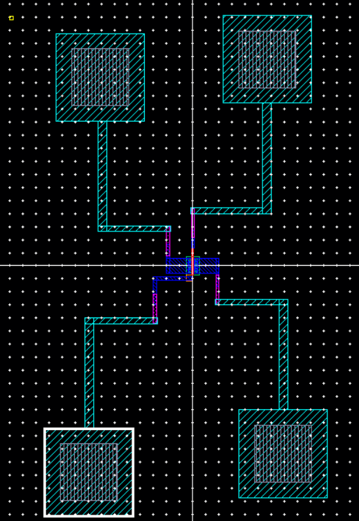
- Lay
out a 6u/0.6u NMOS device and connect all 4 MOSFET terminals to probe
pads (which can be considerably smaller than bond pads [see MOSIS design rules] and directly adjacent to the MOSFET (so the layout is relative small).
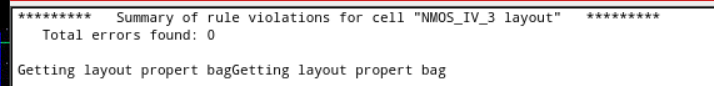
- Show your layout passes DRCs.
- Make a corresponding schematic so you can LVS your layout
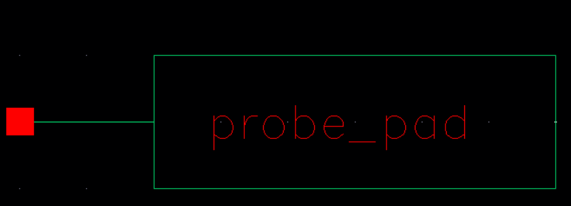
For this part of the lab, I will be creating and using probe pads.
I will create a layout first.
Then a schematic and a symbol.
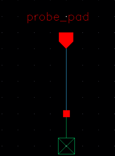
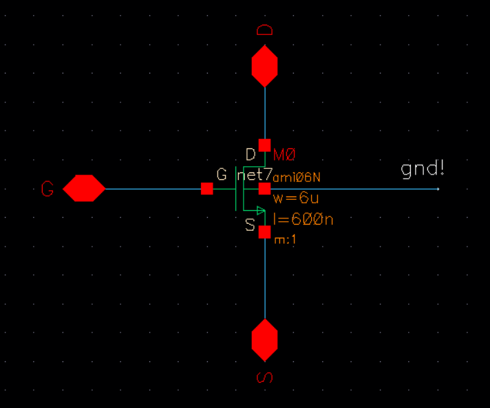
Now, I will create an NMOS schematic with the probe pads.
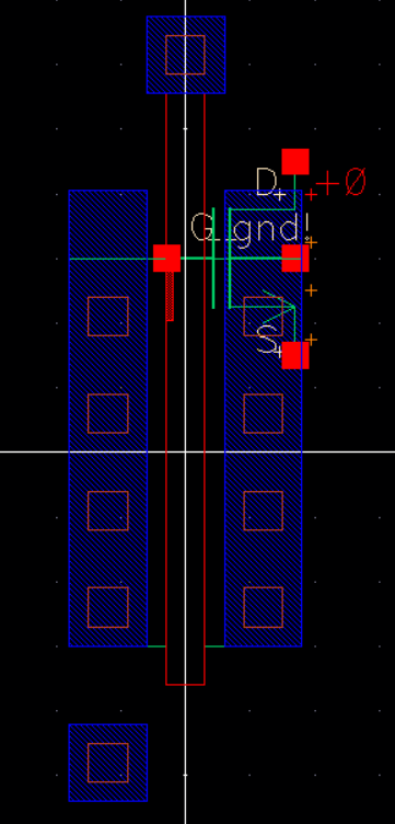
Then I will create a layout of the NMOS with probe pads then DRC.

Now I will extract and LVS.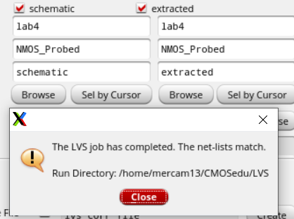
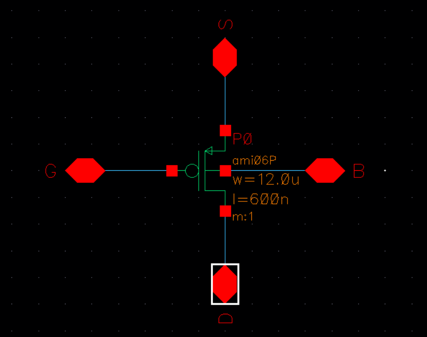
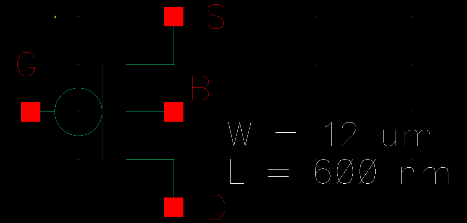
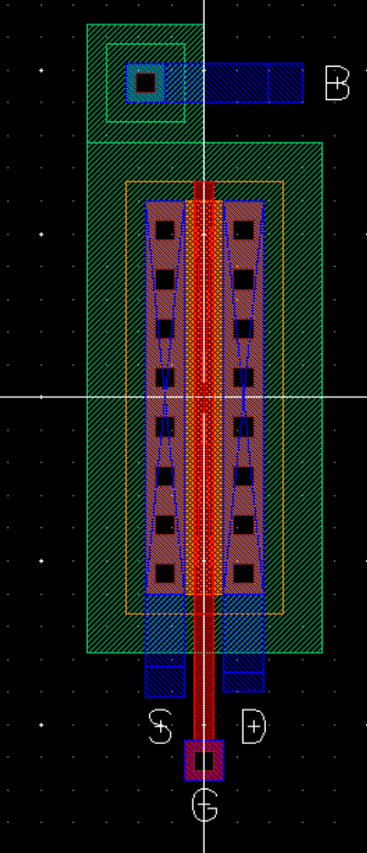
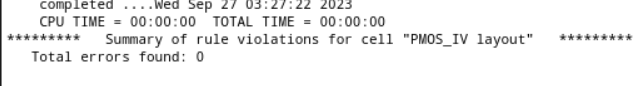
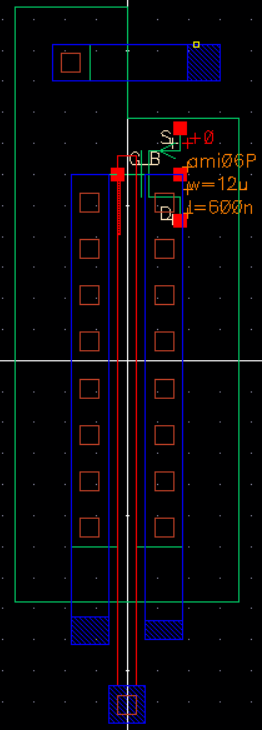
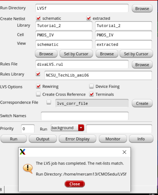
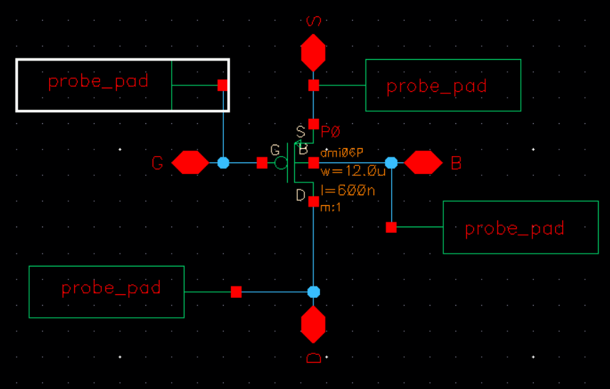
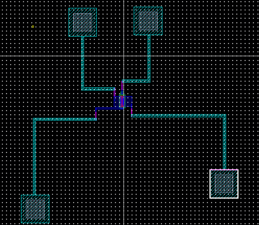
- Lay out a 12u/0.6u PMOS device and connect all 4 MOSFET terminals to probe pads.
- Show your layout passes DRCs.
- Make a corresponding schematic so you can LVS your layout.
Repeat steps from above with PMOS and modifying the parameters to meet 12u/0.6u.
First, create an PMOS schematic with the probe pads.
Then create a layout of the PMOS with probe pads then DRC.

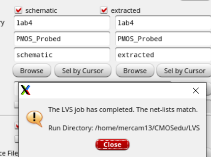
Now extract the layout and do LVS.
Return to EE421 Labs