- Tutorial 5 was completed and lab documentation was reviewed in its entirety in preparation for this lab
- out<3> is connected to a 100fF, out<2> is connected to a 500fF capacative load
- out<1> is connected to a 1pF capactive load, and out<0> is not connected to any load
2.) Design schematics and symbols for an 8 bit in/out array of NAND, NOR, AND, inverter, and OR gates
- provide a few simulations of each
3.) Design a schematic and symbol for a 2:1 MUX/DEMUX device
- explain using simulations how the device operates and can be used for each instance
4.) Design a schematic and simulate an 8-bit word 2:1 MUX/DEMUX device schematic and symbol
- be sure the device only has one select input through the use of an inverter
5.) Draft the full-adder circuit seen in Fig. 12.20 of the CMOS 4th Edition textbook using 6u/600n devices
- create a symbol for the device and then use this symbol to create an 8-bit adder schematic and symbol
- simulate the 8-bit adder device to prove its operation
6.) Lay out the 8-bit adder cell showing DRC and LVS confirmation
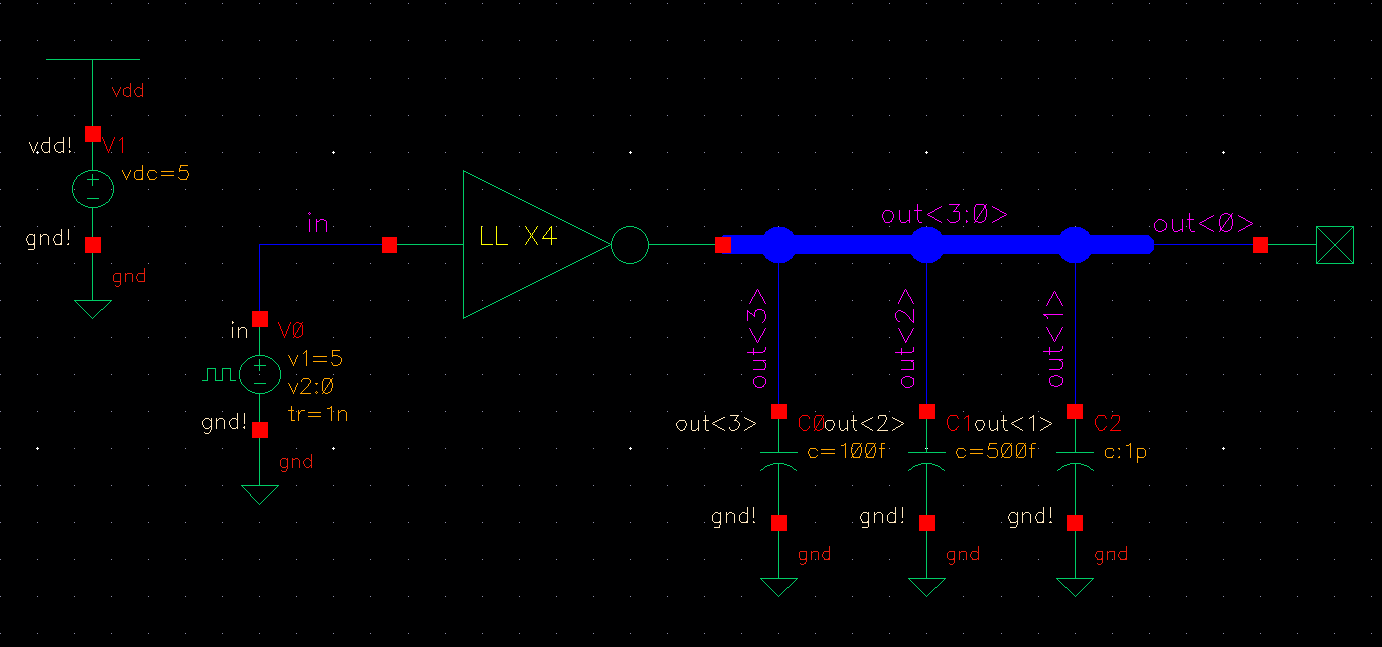
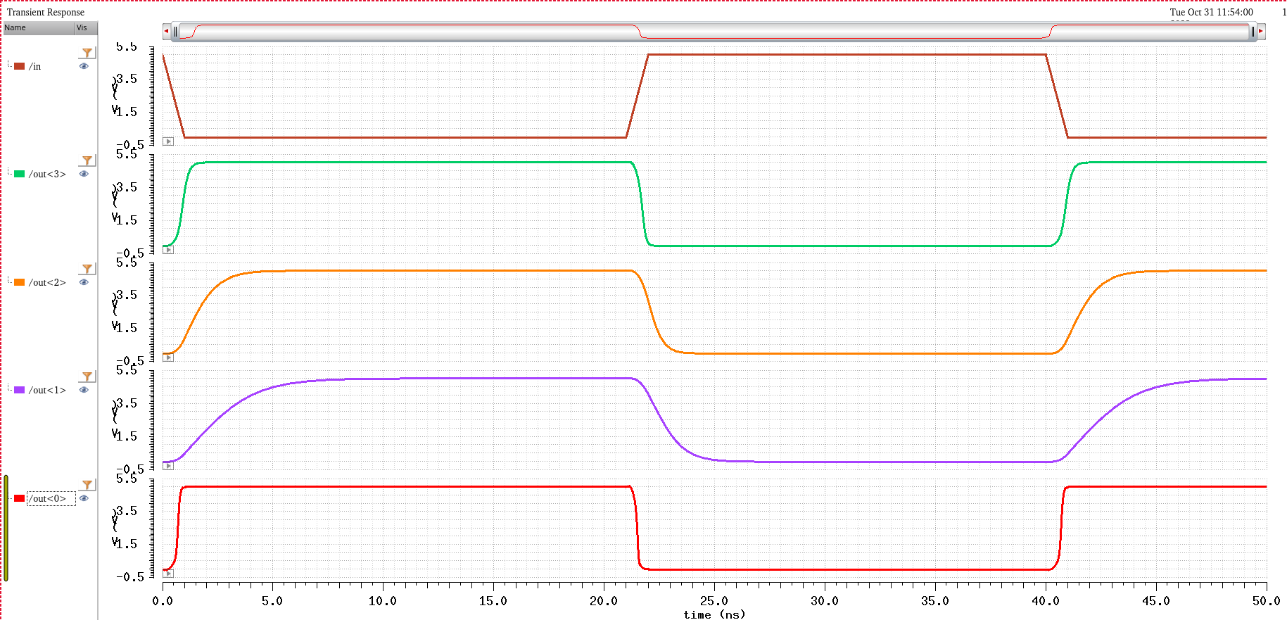
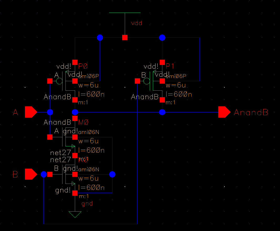
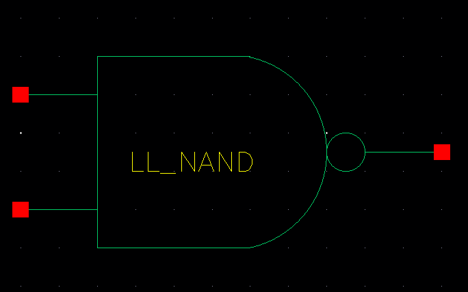
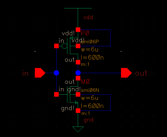
Figure 11-12: single bit NAND gate schematic and symbol
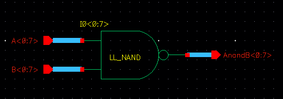
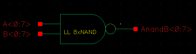
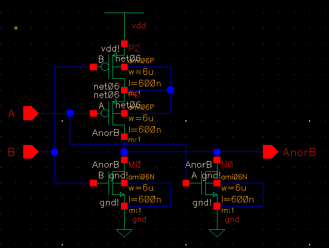
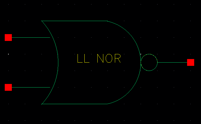
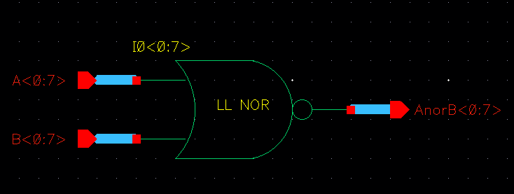
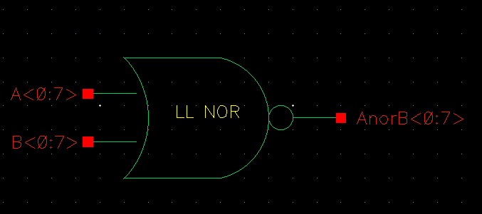
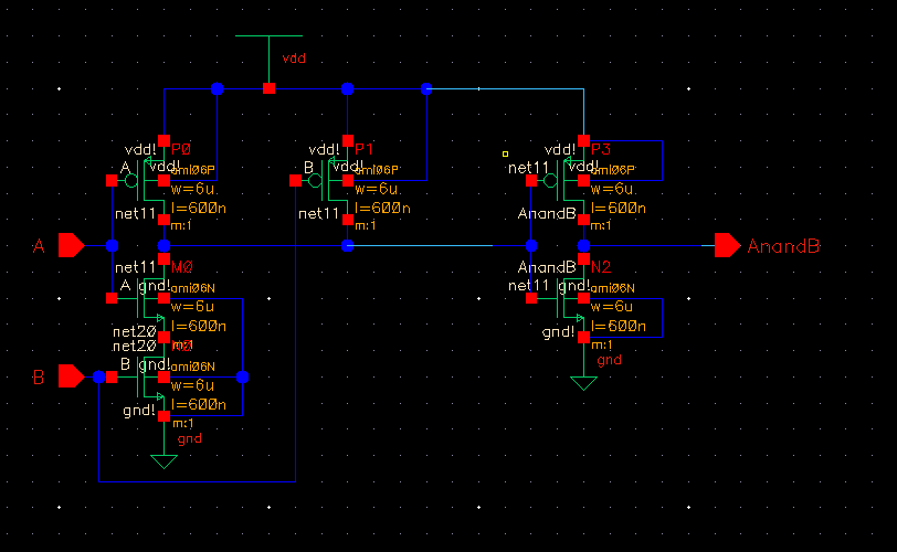
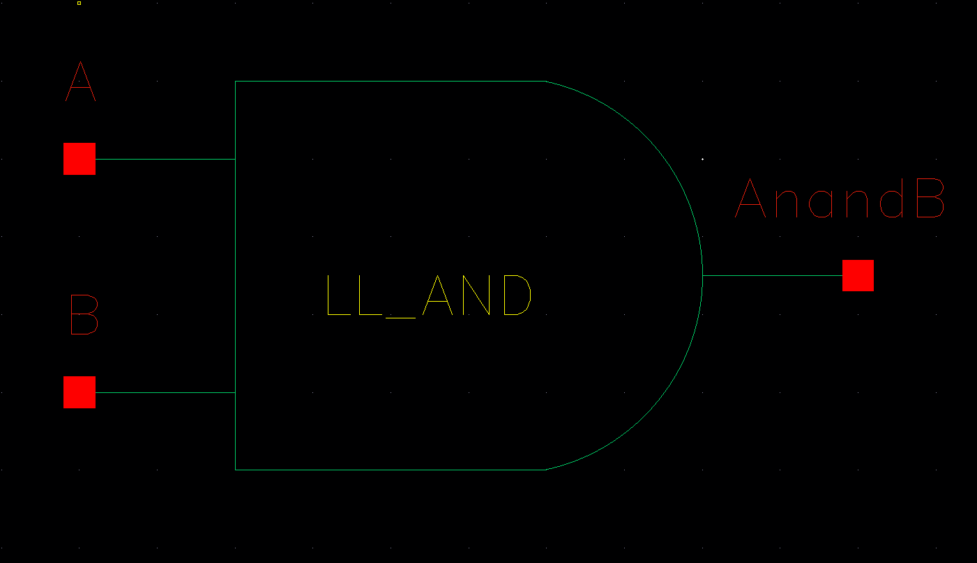
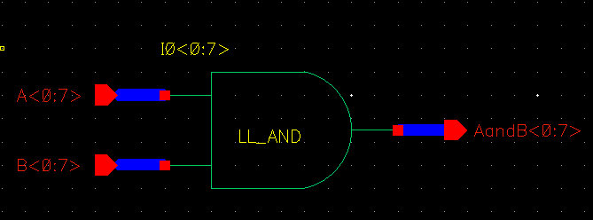
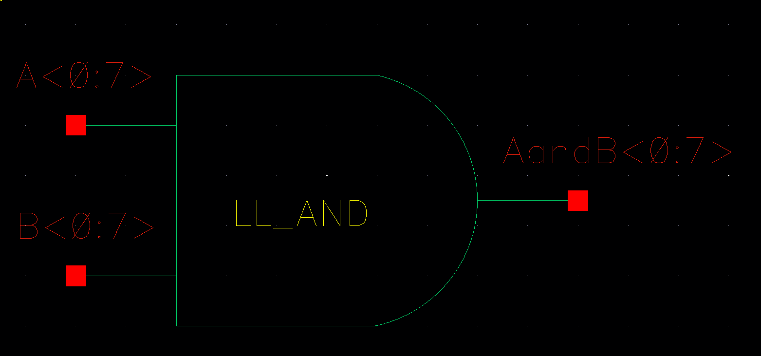
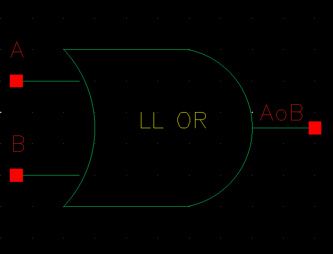
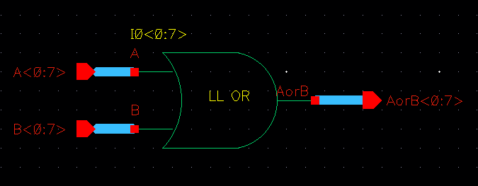
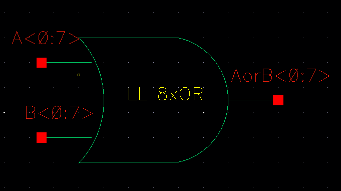
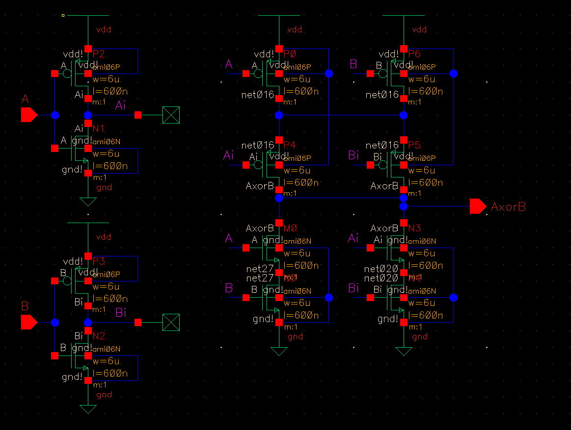
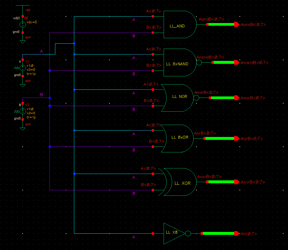
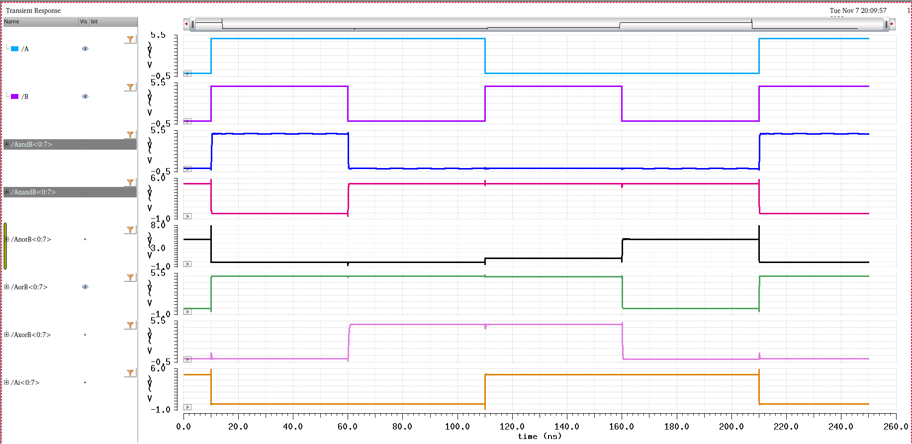
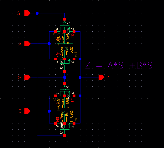
Figure 33: 2:1 multiplexer schematic
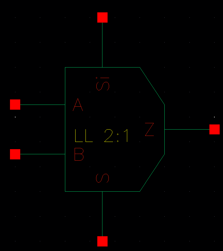
Figure 34: 2:1 multiplexer symbol view
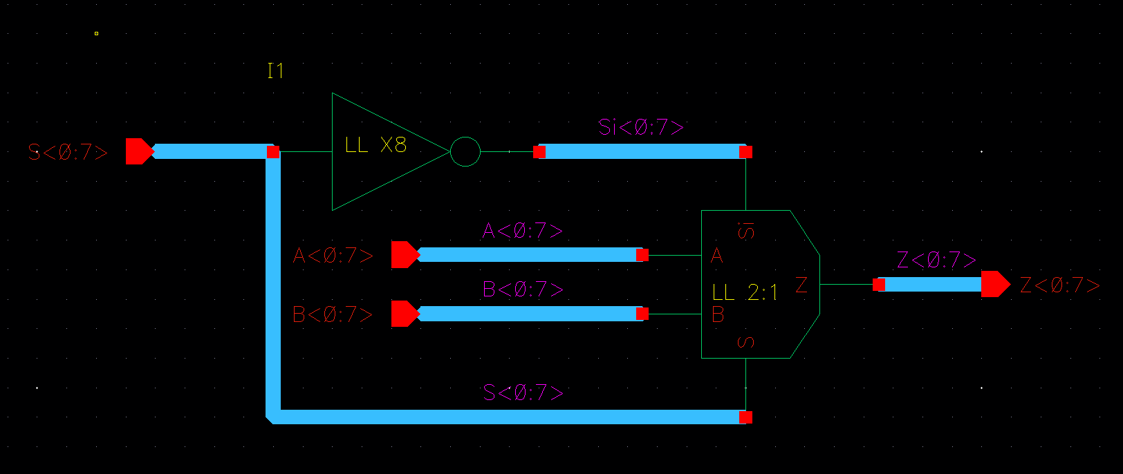
Figure 35: 8-bit multiplexer schematic
NOTE: because we have only two inputs (or outputs when used as a DEMUX) I implemented an inverter to simplify the select circuit and allow a single input to selct the input or output of the device. If this was a larger device, it would require more than one single input select signal.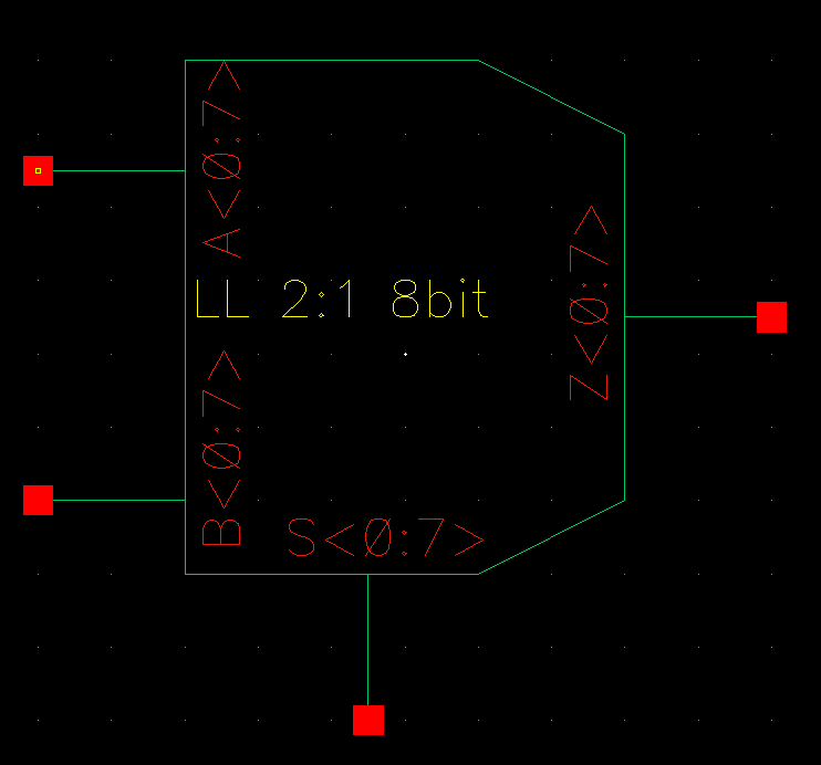
Figure 36: 8-bit multiplexer symbol view
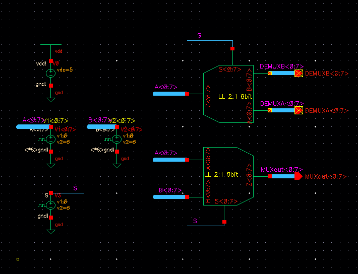
Figure 37: 8-bit multixplexr simulation circuit showing MUX and DEMUX device capabilities
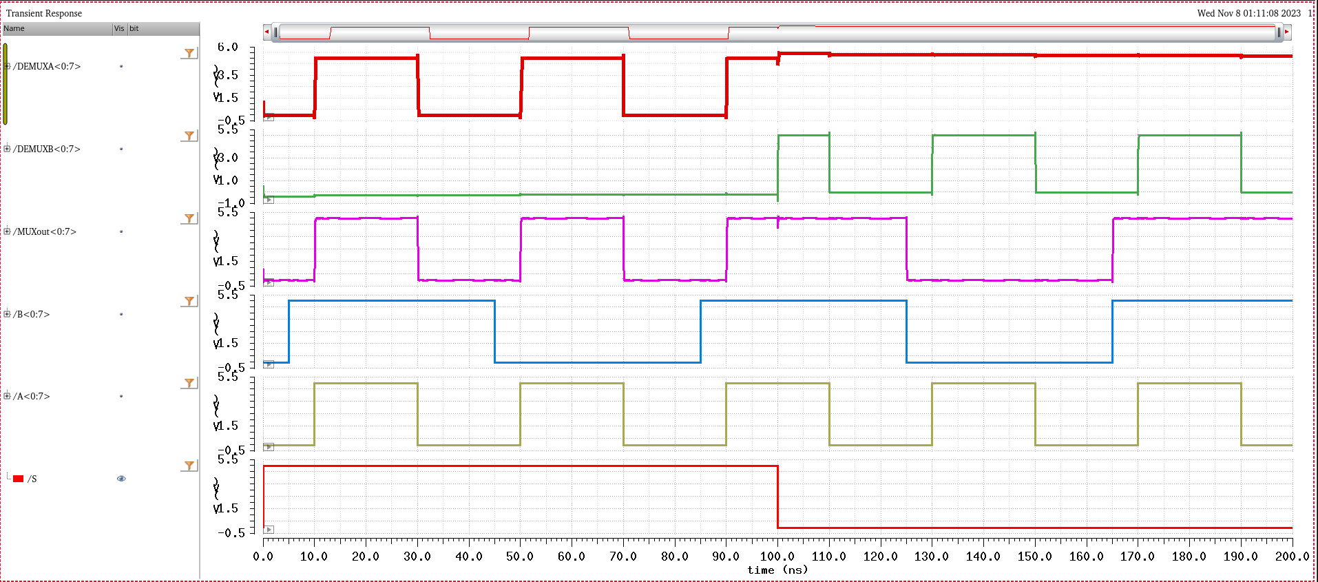
Figure 38: 8-bit MUX/DEMUX results showing proper operation of device properties
NOTE: when reviewing this simulation you can see that while the MUX select input is set to '1', the output recieves the 'A' input signal, and when the input switches to '0' or 'low', the output follows the 'B' input signal. Reviewing the DEMUX results you can see as well while the input select is '1' the 'DEMUXA' output recieves the output wave, and near the 100n area when it switches to '0' the 'DEMUXB' output folows the signal. This device can be used to seperate an input singal to two individual outputs while used in DEMUX, or accept two different inputs (individually) when used as a MUX device. One thing to note is that when the device switched during teh 0-1 transition the output of 'DEMUXA' remained high, this could eb fixed with the addition of a bleed off transistor which would drag the output low once the selection to the other output was made.
AOI Full Adder Device
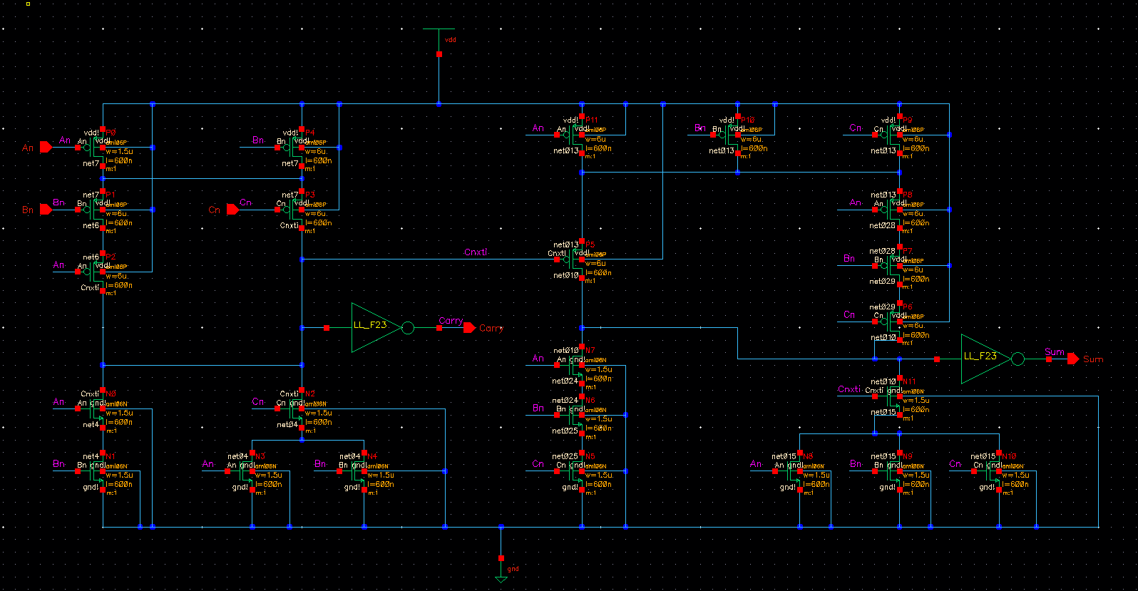
Figure 39: AOI full-adder circuit in CMOS topology from Fig. 12.20 of the course textbook
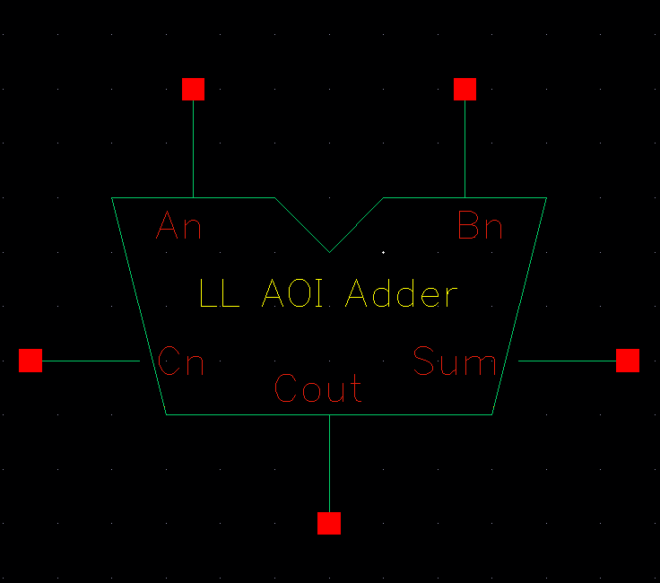
Figure 40: AOI full-adder symbol view
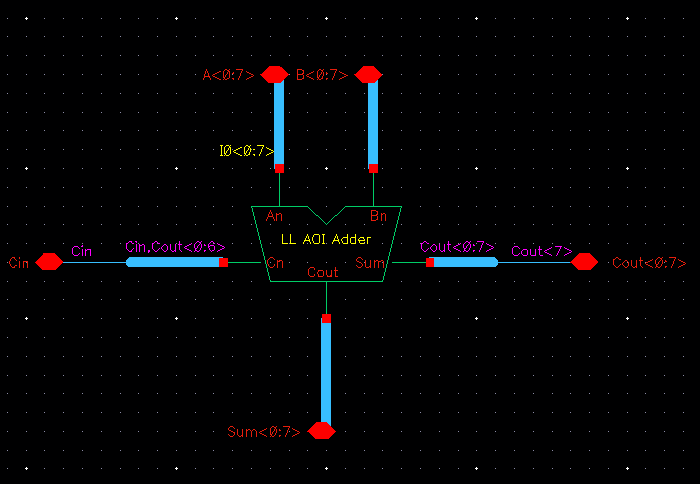
Figure 41: 8-bit AOI full-adder schematic
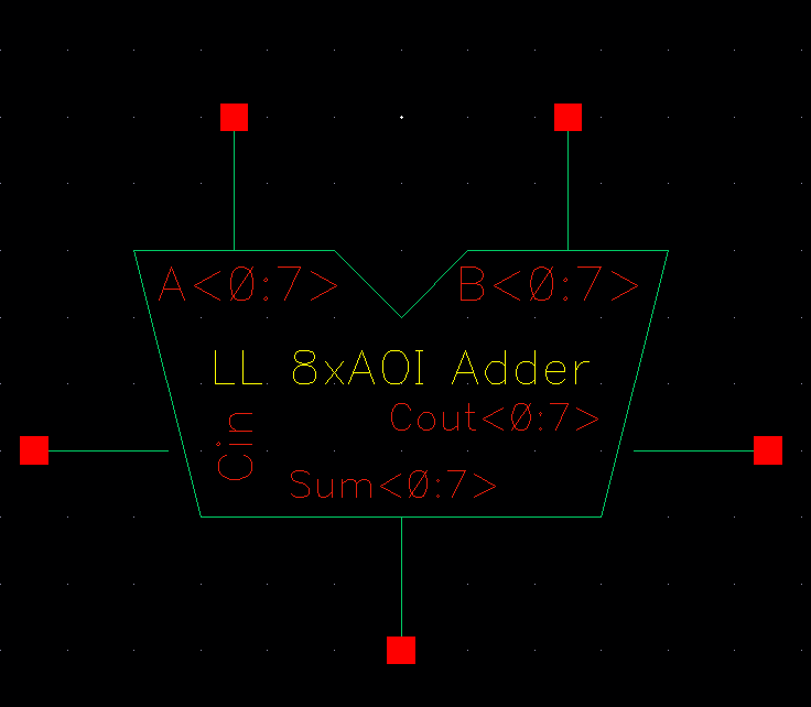
Figure 42: 8-bit AOI full-adder symbol view
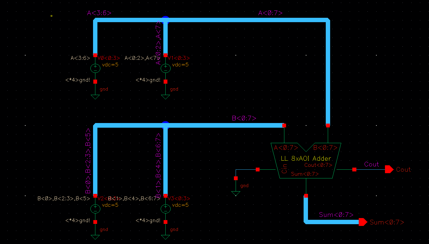
Figure 43: 8-bit AOI full-adder simulation circuit
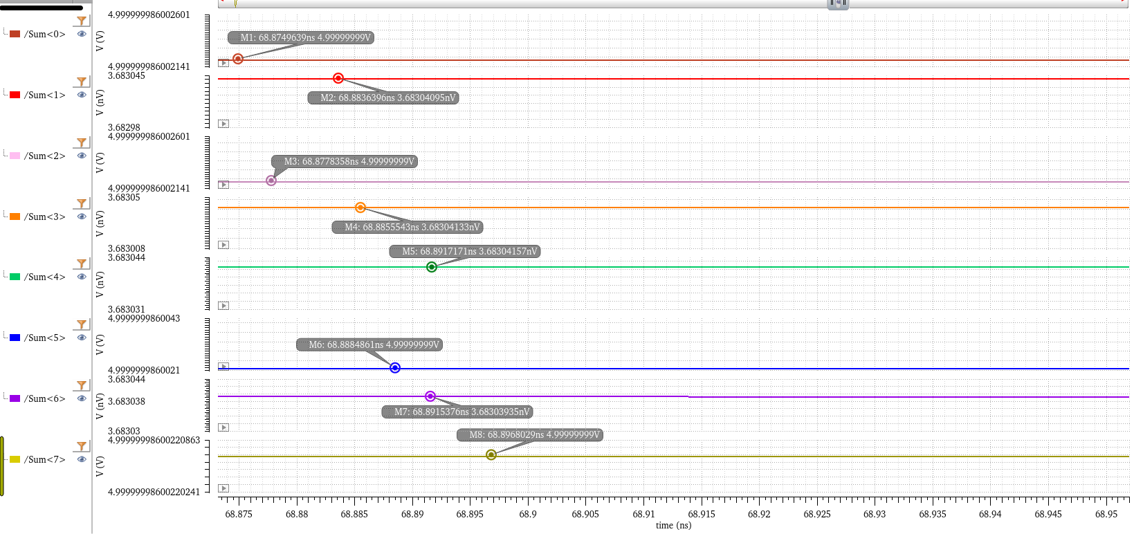
Figure 44: 8-bit AOI full-adder simulation results performed using the Cadence Spectre Simulator
NOTE: in the simulation above two binary numbers were added using no carry input, and gave a correct output response.
A = 01111000 (decimal 120)
B = 00101101 (decimal 45)
Sum = 10100101 (decimal 165)