Digital IC Design - Lab 3 - EE421L

Author: Leonardo Ledesma 

Email: ledesl1@unlv.nevada.edu

September 19, 2023


Lab Description

- This lab will focus on the layout of  10-bit digital to analog converter (DAC) designed in the previous lab


Pre-Laboratory Procedure

- I have backed up all previous work from the lab and course

- Tutorial 1 was completed


Laboratory Objectives

1.) Layout a 10K resistor as seen in Tutorial 1

2.) Using the 10K resistor, lay out the 10-bit DAC designed in the previous lab

- all input and outputs should use metal 1, and be parallel resistors are to be laid out in a relative x-position with varying y-position

3.) Show DRC and LVS confirmation including extracted layout view

4.) Provide a .zip file of the design directory in the lab3 directory, including a link to this lab report for grading purposes


Laboratory Procedure

The lab begins with the layout of a 10K resistor using the Cadence C5 process. For this process we must note that N-well resistance is 800 ohms per square. Performing hand calculations will be necessary to determine our correct resistance value. 

 
We begin by determing the proper sizing for the resistor using the hand calculations below.

Eq 1: Hand Calculations
             

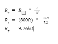
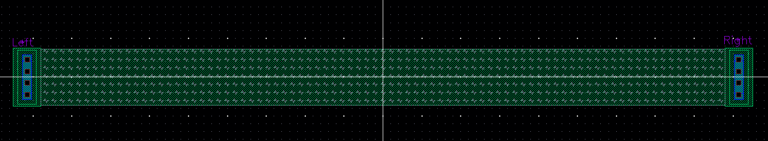
Figure 1: 10K resistor layout


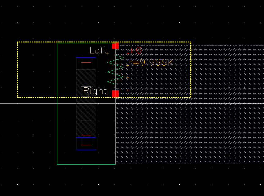
Figure 2: 10K resistor extracted view verifying correct value


Moving on the 10K resistor will be used to create a single bit DAC circuit which will then be instantiated 10 times to form the 10-bit DAC layout. Below is a single bit formation using 3 of the previously shown 10K resistors. Care was taken to be sure the resistors were stacked in alignment of the x-axis to make the layout of the 10-bit DAC easier. 

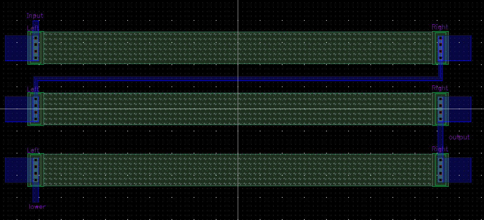
Figure 3: Layout of single bit DAC 


The single bit layout is then ran through a design rule check (DRC) to confirm it meets the process' requirements for sizing and spacing. Below you can see the DRC confirmation for the single bit DAC with no errors. This portion was also extracted and LVS confirmation was determined before moving on to the full 10-bit design.


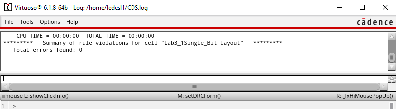
Figure 4: DRC confirmation for single bit DAC portion


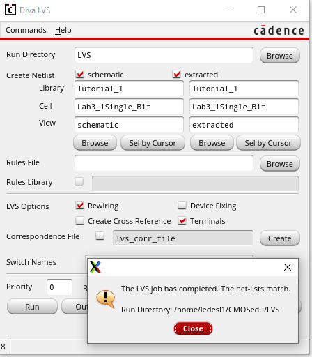
Figure 5: LVS confirmation for single bit DAC circuit


The single bit DAC portion will now be used 10 times to create a 10-bit DAC. Using metal 1, connections will be made between each instantiation to build the full 10-bit circuit. The overall design will involve the use of 31 10K resistors. Below we can see the final circuit design in layout format showing LVS confirmation.

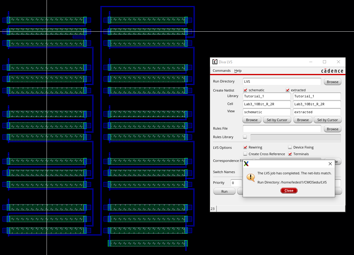
Figure 6: Full 10-bit DAC layout view with LVS confirmation


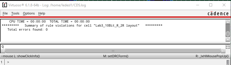
Figure 7: Full 10-bit DAC circuit DRC check complete with no errors


Again we see the circuit below in extracted view of the entire 10-bit DAC using the C5 process. 


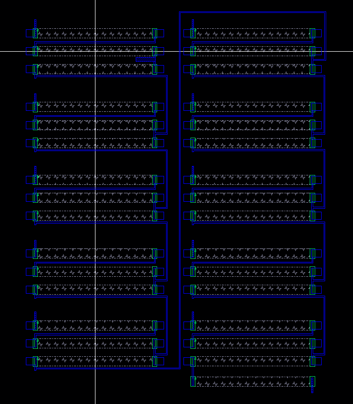
Figure 8: Full 1-bit DAC extracted view


I can conclude that through the layout, extraction and simulation process, my 10-bit DAC performed as expected and achieved the outcome this lab was requesting. 


lab3.zip Cadence Files Location

All layouts, schematics and extracted content pertaining to this lab can be viewed in the file attached below

Lab3.zip


Backup Confirmation

As with previous labs, all files were backed up during the process of completing this lab.


Return to EE421 Labs