Final Project - EE 421L
Project (NOT a group effort) – design a non-inverting buffer circuit that presents less than 100 fF input capacitance to
on-chip logic and that can drive up to a 1 pF load with output voltages greater than 7V (an output logic 0 is near ground
and an output logic 1 is greater than 7V). Assume VDD is between 4.5V and 5.5V, a valid input logic 0 is 1V or less, a valid
input logic 1 is 3V or more. Show that your design works with varying load capacitance from 0 to 1 pF. Assume the slowest
transition time allowed is 4 ns.
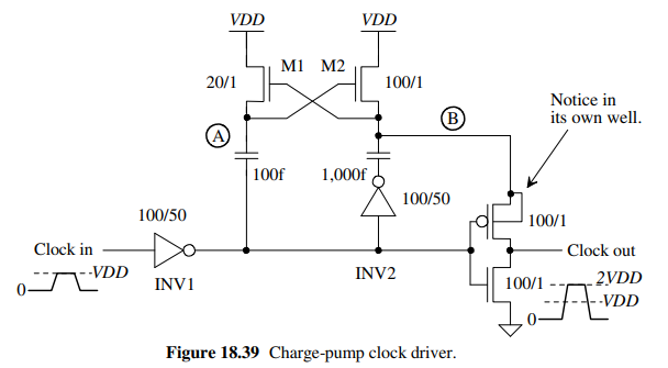
For this project, I was instructed to use Figure 18.39 -- a charge-pump clock driver schematic -- as a starting point.
For reference:
This topology is a good fit for this project because it is suited to output a voltage greater than VDD + Vthn, which would range
from about 5.2V to 6.4V or so. This buffer needs to output at least 1.8V higher than this.
To briefly summarize how it works, the voltage at B will swing from VDD when the input is low to 2VDD when the input is high,
by way of the M2 mosfet. When the input does swing high, the output inverter will see a 0 on its input, so the PMOS will turn on
and B's 2VDD will be pulled down through the output and delivered to the load. At this point B is isolated from the power supply
though, so that's why we need a large capacitor there so it can support a decently long output pulse.
Now, to modify this design:
First, the buffer must present less than 100 fF of input capacitance. This limits the size of the first inverter used in the design.
Input capacitance is given as
(3/2)(Coxn + Coxp) = (3/2) * Cox' * (Ln * Wn + Lp * Wp).
I decided to fix Wp = 2*Wn = 2W (so Vsp is roughly VDD/2) and a minimum length of L to get the equation
(3/2) * Cox' * (LW + 2LW).
Substituting in values Cox' = 2.5fF/um^2 and L = 0.6um,
(3/2) * 2.5fF * (1.8W) = 6.75fF * W.
Since my input capacitance must be less than 100fF, I was able to solve for W with
W <= 100fF / 6.75fF = 14.8 um.
This gave me my constraint for the size of the first inverter. I decided to use a W = 12um, which with my L = 0.6um from before
gave me an inverter of size 24u/12u.
Next, I needed to pick reasonable sizes for the on-chip capacitors. As this buffer was required to drive capacitances up to 1pF, I
picked that as my load capacitor value and used this equation (derived from a model of a switch closing between Cr and Cload) to
calculate a sufficient value:
Vf = ( Cr / ( Cr + Cload ) ) * 2 * Vi,
where Vf is the voltage I wanted to exceed at the output (7V) and Vi is the minimum supply voltage I expected to have to work with (4.5V).
Thus, 7V = ( Cr / ( Cr + 1pF) ) * 2 * 4.5V, or Cr = (7/2) * 1pF,= 3.5pF. I decided to increase this to 4.5pF to ensure that the voltage
would still be able to rise above 7V in case of any parasitics or other unexpected effects.
Note that at the upper end, this formula would instead show Cr = (7/4) * 1pF = 1.75pF.
This shows how less capacitance is required when there is less difference between the input supply and the 7V minimum output.
I left the value of the 100f capacitor below node A alone because this capacitor isn't ever delivering charge to the output.
Final capacitor sizing:
I was originally going to size the two capacitors to be 100 fF and 4.5 pF, but after running some simulations using NMOS capacitors
instead of the standard capacitor components, I found that these capacitances needed to be larger in order to operate the charge pump.
From my experimentation, I found that a small NMOS capacitor of 1.44 pF and a large NMOS capacitor of 9.00 pF worked in order to
deliver the delays that I found satisfactory. I did run simulations of the NMOS capacitors outside of the design and confirmed that they
did have (allowing for some parasitics) the same capacitance as given by the Cox formula mentioned prior.
As far as reasons why the NMOS capacitors didn't quite function the same as the ideal capacitors, I suspect body effect played a significant
part. Since the bodies of these two MOSFETs are tied to ground and the S/D voltage (ClkOut, in my schematic) varies from 0 to VDD, there
would likely be a parasitic capacitance between the bottom plate (formed by the source, drain, and channel of the MOSFETs) and the substrate
serving as the body terminal.
Small capacitor sizing, 1.44 pF:
C = Cox' * W * L, so 1.44pF = 2.5fF/(um^2) * W * L, or W*L = 576. Taking the square root
of 576 left me with W = L = 24um, which conveniently already aligns with the 0.15 grid spacing.
Large capacitor sizing, 9 pF:
9000/2.5 = W * L = 3600 um^2. The square root of 3600 is 60, so I used W = L = 60um.
Next I needed to pick the other two inverter sizes. Both needed to be sufficiently large, as one would be responsible for driving the load
capacitance and the other would be responsible for driving the large MOSFET capacitor, which in this circuit will be at least 9 times larger
than the load (9pF vs up to 1pF). To ensure reasonable delays without compromising the size of the final layout, I decided to pick a size of
60u/30u for both.
Finally, I adjusted M1 and M2 to match proportions (24u/0.6u and 4.8u/0.6u) with the input inverter (100/1 --> 24u/0.6u).
Here is the schematic I created for this circuit. I will elaborate on the different symbols used as well.

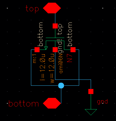
This is the schematic for the small NMOS capacitor. Note the sizes of 12u/12u and
the fact that the body is tied to ground. The large NMOS capacitor schematic is identical
to this one, but with a size of 60u/60u as indicated in the symbol.
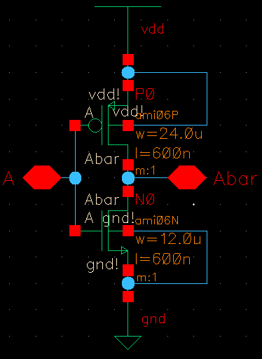
This is the schematic for the small input inverter.
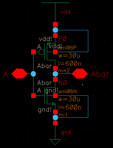
This is the schematic for the large inverter which feeds into the large capacitor.
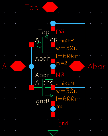
This is the schematic for the output inverter, which notably has a PMOS body not tied to VDD.
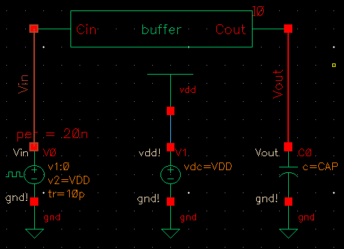
Here is the schematic I used for my simulations. Note how I used design variables VDD and CAP in the schematic to make it
easier to simulate and perform parametric analysis.
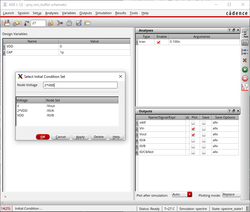
Here is how I set up the ADE for most of the simulations. Here was where I set my static (non-parametric) design variables
and set initial conditions to help the circuit simulate properly.
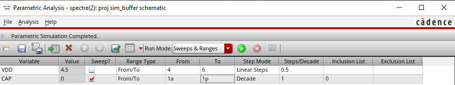
Lastly, here is how I set up the parametric analyses for my simulations. For each set I usually set a given load capacitor
value and then swept over the range for VDD, but for one plot I set VDD to 4.5V and swept over a wide range of
capacitor values instead.
Simulations:
These first two plots are the results for the maximum load capacitor of 1pF.
Here we can see the output value for each input signal, taken at the 4 nanosecond benchmark.
Each signal is able to rise over 7V by this point, satisfying the design constraint.
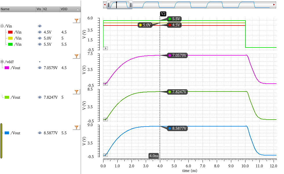

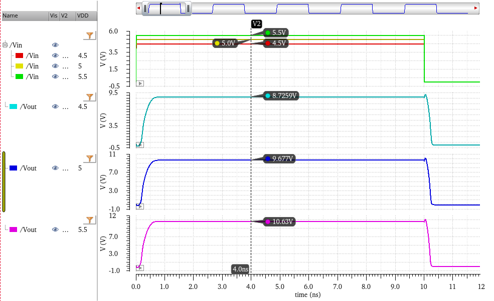
Now here are the same results for a 500fF load capacitor. They follow the same trends, but the outputs peak higher and the transition
times are much faster. Note that the voltages at 4ns are roughly 0.8 to 1V higher than the previous 1pF results.

The rise and fall delays are also much smaller, as shown in this plot: (Click for a larger view)

Now with no load capacitor at all (CAP = 0), we see that we obtain the maximum voltage gain and shortest delays possible with this circuit.

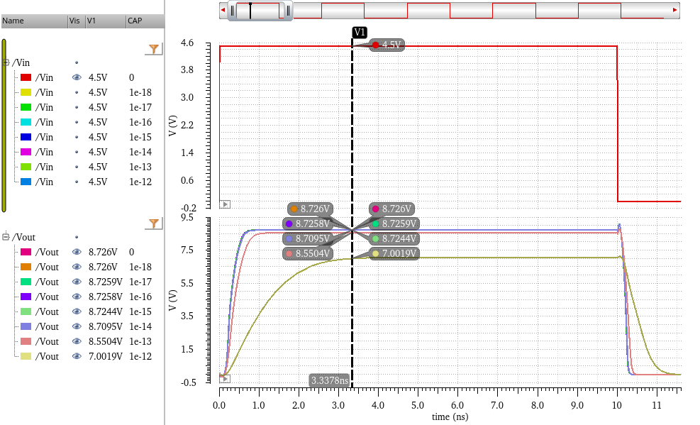
I also ran one parametric analysis where I kept VDD fixed at 4.5V (lower supply voltages would show the worst case scenario) and then
varied CAP between 0 and 1pF. Please click the plot to see a larger version with two vertical lines shown. With these lines, I indicated
that at this time (3.3378 ns < 4 ns) all of the possible output signals with a 4.5V supply had successfully passed the 7V mark. We also
see that for load capacitor values of 10 fF or less the different Vouts start to converge to the same curve.
These analyses show that this circuit can successfully boost an input clock signal up to 7V with input clock and supply ranging from 4.5
to 5.5 volts. The buffer can drive its output over a load of up to 1pF with less than 4ns transition time in each direction. The buffer also
presents less than 100 fF input capacitance.
Part II -- Layouts
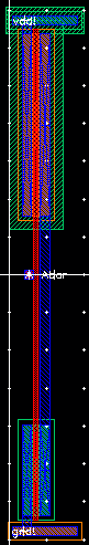
First, I laid out my NMOS capacitors, as they were my largest components.
Large:
Small:
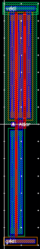
After that, I laid out the inverters. I made the layouts correspond
in terms of vertical space so they would be easier to connect later.
Small: Large: Output:
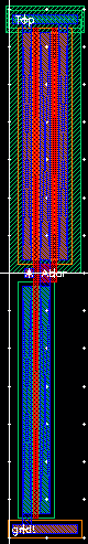
There are also two independent NMOS devices in this design that I decided to implement
directly in the final layout, instead of making symbol views for normal NMOS instances.
Overall design:
As a reminder, here is the final schematic.
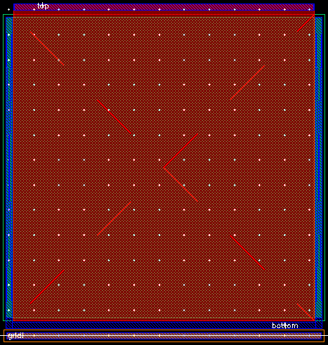
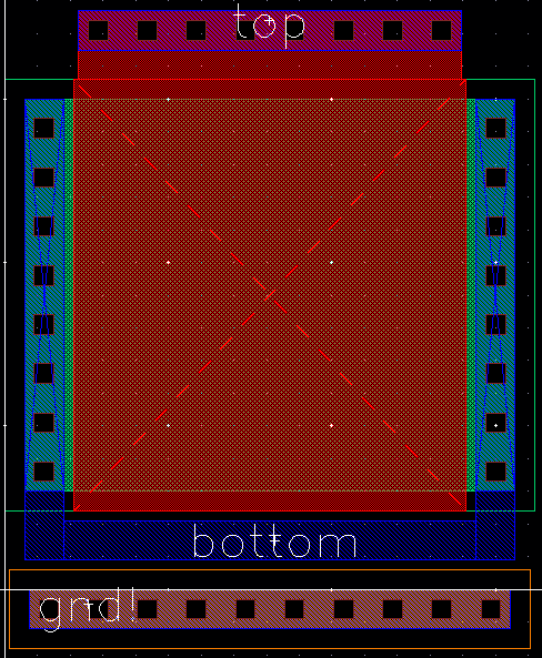
Here is the final rendition of my project layout, after I put all of the pieces together.

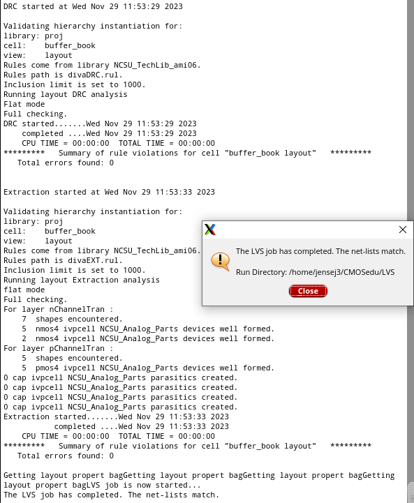
Finally, here are the design rule verification results:
Directory archive for this project: