Lab Project - ECE 421L
Design Parameter Selection
***************************************************************************************************
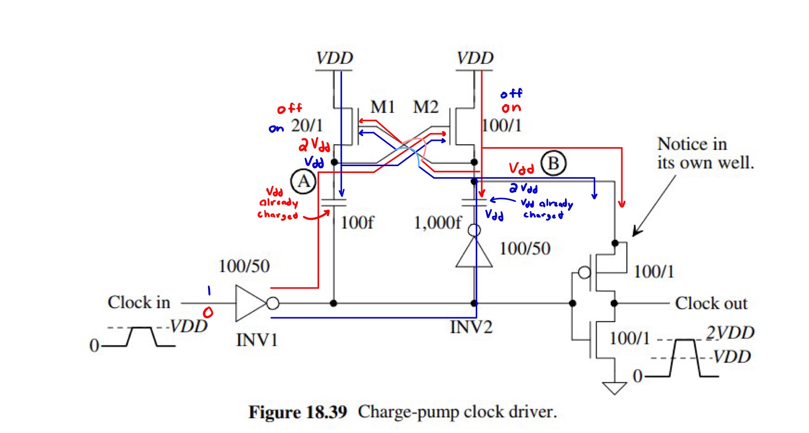
To begin, we must choose our design parameters, this is based on the charge pump circuit, which can be thought of as 2 parts.
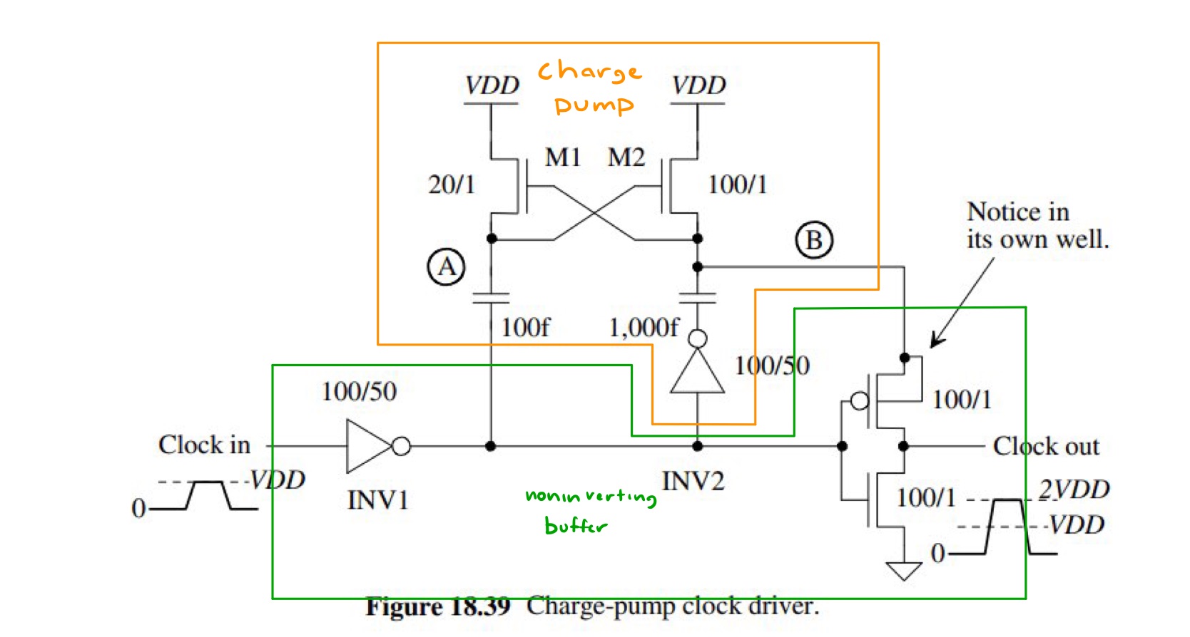
The noninverting buffer part works by adding some delay to some input. We notice 2 gates here, the leftmost inverter and the rightmost inverter(not INV2).
The charge pump part allows us to output greater than 7V. This uses capacitors(Node B) that charge during logic 0 up to VDD and provide VDD to the rightmost inverter.
And during logic 1 those same capacitors will discharge the voltage(VDD) and extra voltage(another VDD) provided by INV2 in order to provide 2VDD to the rightmost inverter.
And with the circuit marked up to where the path of the voltage goes.
****Note****
This circuit requires a few pulses to work as intended, during the first few pulses, the capacitors connected to node A and node B have not been able to fully charge to VDD. The circuit will appear to be working during simulation, however the voltage requirements would not be met. We will notice in the simulations that after a few pulses, the output voltage is at a consistent value.
************
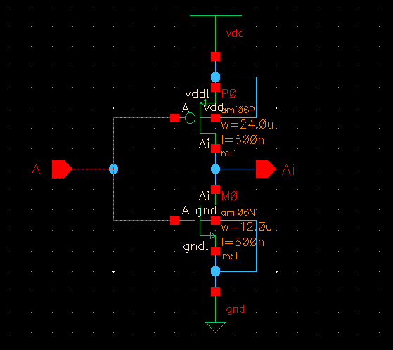
First let's begin with selecting INV1, INV2, and the rightmost inverter. For ease/simplifcation of design, I decided to select all three of these inverters to be the same size.
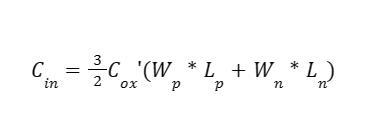
To verify that we are under 100fF capacitances, we begin with this equation to determine the parameters of the mosfets. As we can notice in the figure above, there is only one point of input, which is the input of the INV1. So we simply must calculate our equation by....
Now there is no requirement that the 2 transitions times are the same, other than they are both under 4ns. However it was my design choice to make Tphl and Tplh as well as Tr and Tf the same. To do that Wp = 2Wn. Additionally, Ln = Lp = 0.6u, in order to minimize large horizontal layouts later on.
Which after setting all those variables we get...
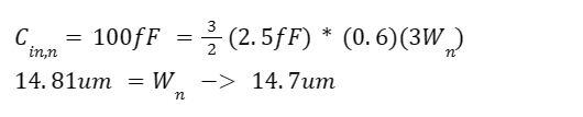
Now we could stay at Wn = 14.7um and set Wp = 29.4um, but let's assume that for whatever reason there are possible manufacturing errors or other hypotheticals that could cause our input capacitance to be over 100fF.
So let's reduce our Wn and Wp down to Wn = 12um and Wp = 24um. Which will still satisfy the less than 100fF input requirement and gives us a small buffer of design in case someone is adding extra capacitance for whatever reason. And Ln = Lp = 0.6um.
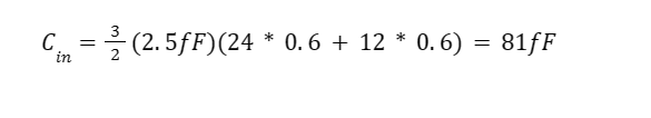
So the parameters of the first INV1, INV2 and the rightmost inverter to the output are:
Wn = 12um, Wp = 24um
Ln = 0.6um, Lp = 0.6um
Next, why choose PMOS width to be double the size of NMOS for the inverters?
As previously stated, choosing double the width allows:
- Tr and Tf to be the same
- Tplh and Tphl to be the same.
Why? Well, R'n = 20k ohms and R'p = 40k ohms. Hence when calculating transition times, doubling the width of the NMOS for the PMOS means same resistances, seen below.
Next let's verify that these lengths/widths will satisfy the 4ns requirement.
Beginning with calculating the resitance... and then the transiton times...
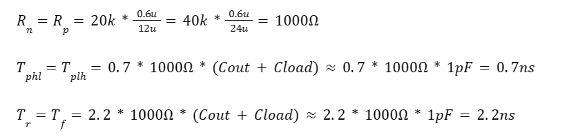
Cout is omitted since the 1pF load is much greater than the output capacitance.
Cout would be the capacitance of the final inverter.
And as can be seen, the under 4ns transition time is satisfied.
Additionally, choosing double width isn't just for same transition times. By selecting Wp = 2Wn, we can ensure that the switching point voltage is always 1/2 of VDD. This was showcased in a prior lab
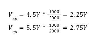
And we can use the simplified equation version to calculate Vsp:
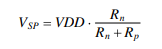
Which when testing with the max VDD and min VDD then these would be the switching point voltages...
These clearly satisfy the LOW <= 1V and HIGH >= 3V.
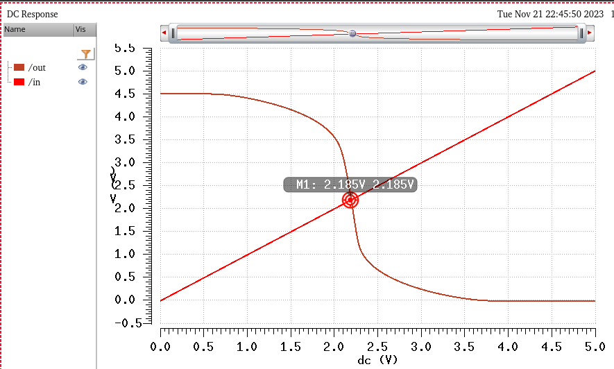
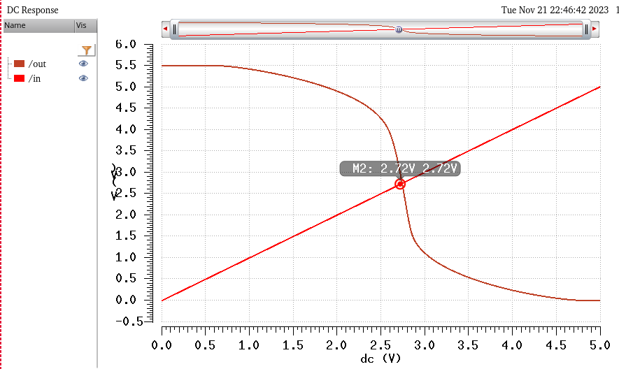
And these are the simulations to prove that indeed the inverter's switching point will work as hand calculated. (The inverter schematic is in the next section)
First is VDD = 4.5V
And then VDD = 5.5V
Next to determine M1 and M2 of the figure above.
For simplicity of design and being able to duplicate same layout later on, I chose M2 to be the same NMOS size as 12u/0.6u.
It should be noted that an even wider NMOS, like the figure's own
60u/0.6u NMOS would have an advantage by charging the capacitors even
faster. But again for simplicity, the same size was chosen from the NMOS in the inverters.
Then M1 is chosen as the minimum possible parameters allowed by C5, so M1 is 1.5u/0.6u. This is to reduce the size of this NMOS's layout.
Next deciding on the capacitor sizes at node A and node B.
Again, in order for simplicity reasons and layout duplication, the capacitor at node A is 18fF, using a mosfet of 12u/0.6. Same sizes as the inverters.
For the capactior at node B, since we want to be able to output 7V to a capacitance load of 1pF. Then the capacitor of node B must be sufficienctly large enough to store enough charge in order to be able to drive 2VDD into the final right inverter. So after testing and slowly increasing the capacitance up, I chose a capacitor on node B to be of 5pF, with a mosfet of 45u/44.4u. These values were chosen so that the layout of this mosfet would be close to a square, no reason for this, I just thought square might look best in the layout. There will always be a large capacitor layout no matter what, unless load capacitance is very tiny. A larger load capacitance will require an even larger node B capacitor.
This capacitance can be proven via the following equation and figure:
(Ignore the capacitance and the time when the switch is closing, simply the figure is to showcase 2 capacitors charge sharing, with the switch representing when M2 is on/off)
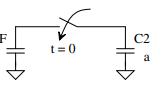
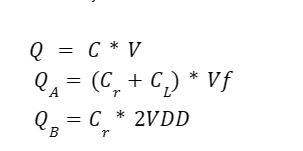
Cr is the left inverter (what we are solving), and Cl is the load (ranging from 0 to 1pF, 1pF used as it is the the value that will have the highest amount of charge sharing)
Qa is the charge when the switch is closed, which is when 2VDD is being provided to our final inverter, outputting 7V (After switch close)
Qb is the charge when the switch is open, (Before switch close)
The charge can't magically disappear, it wants to go where the load capacitance is, and because this new capacitor is introduced, then the charge will attempt to balance between the two capacitors to equalize.
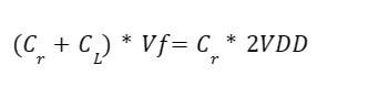
And when we solve for Vf we get....
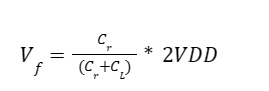
which is basically a voltage divider. Next we know from the design specifications, that the output voltage must be greater than or equal to 7V.... so Vf = 7V. As well, the minimum VDD (4.5V) would have the lowest potential output voltage, so we test with those in the equation above and get....
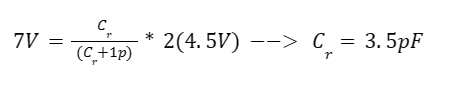
So the absolute minimum capacitor we could use was a 3.5pF. 4pF still has Vf close to 7V, so I chose to just round up to the next integer of 5pF. Which when estimated....
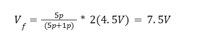
So there's about half a voltage of design buffer from the requirement.
The capacitor at node A and M1(NMOS) are only dealing with powering M2(NMOS) on and off, thus the capacitance and NMOS size can be small. Hence the selection for minimum size for M1 and just copying previous inverter sizes for the capacitor.
So now we have decided every single parameter. Summarized below for simplicity.
All inverters: 24u/12u
Capacitor at node A: 18fF using a 1.5u/0.6u mosfet
Capacitor at node B: 5pF(4.95pF) using a 45u/44.4u mosfet
M1: 1.5u/0.6u
M2: 12u/0.6u
Circuit Schematic
***************************************************************************************************
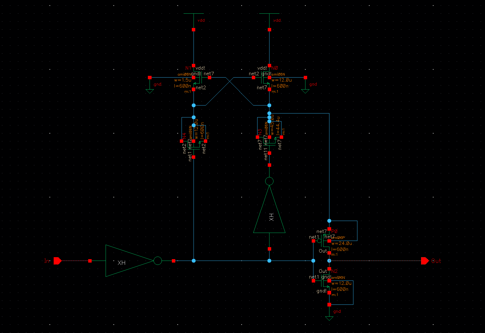
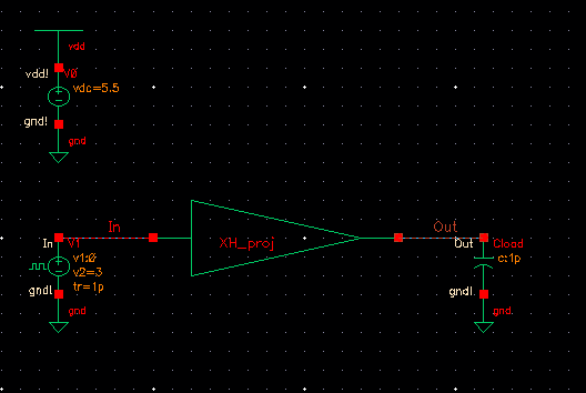
Now we implement all the designs parameters into our circuit schematic for the charge pump clock driver + noninverting buffer.
First here is the 24u/12u inverter schematic.
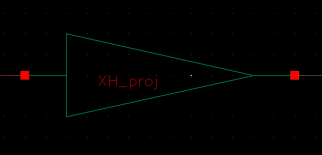
And then that inverter with it's corresponding symbol is used in the full circuit. With all the appropriate parameters as discussed in the previous section.
And here is the corresponding symbol
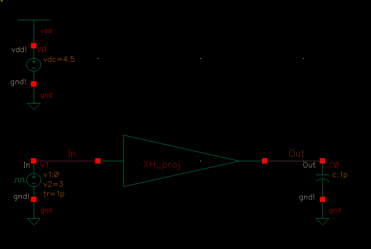
Schematic for Circuit Simulations.
***************************************************************************************************
First off, using the symbol in the above section, now we will use it in the circuit schematic below. Ignore parameters of VDD, load capacitor, and input voltage for now.
Simulating with varying VDD
***************************************************************************************************
One of the requirements is that the circuit will work with VDD ranging from 4.5V to 5.5V. So let's beging simulating our circuit using a 5V input pulse, and 1pF load. Where we vary VDD, below are simulations using VDD = 4.5V, 5V, and 5.5V, testing the extremes and the average. Note the rise and fall times will be proved with this sub section. The 1pF load will lead to the highest rise/fall times, so when I simulate with smaller varying capacitances in the other simulations. it is known that those rise and fall times will always be smaller than the ones found in this section,
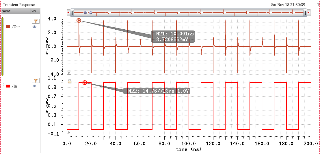
Simulating with VDD = 4.5V
^^^^^^^^^^^^^^^^^^^^^^^^^
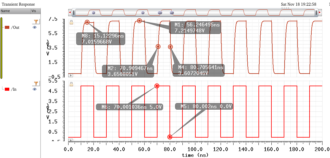
Starting off, we can see that we are in fact outputting to the required 7V or more, 7.2V in this case.
Also as previously discussed, we can see that the first pulse has smaller voltage since the capacitor going to node B is not fully charged to 2VDD. So we can see that a few pulse iterations are needed for the circuit to work as intended.
Next, we can see that the transition times are very close to the hand calculated(0.7ns) transitions.
From the sim above, Tplh = 0.9ns, and Tphl = 0.7ns. So that design requirement is also satisfied.
And the corresponding rise/fall times which again satisfy the <4ns requirement.
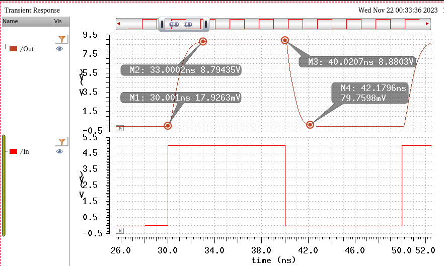
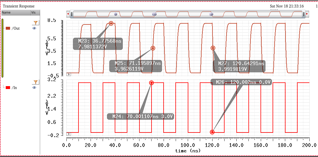
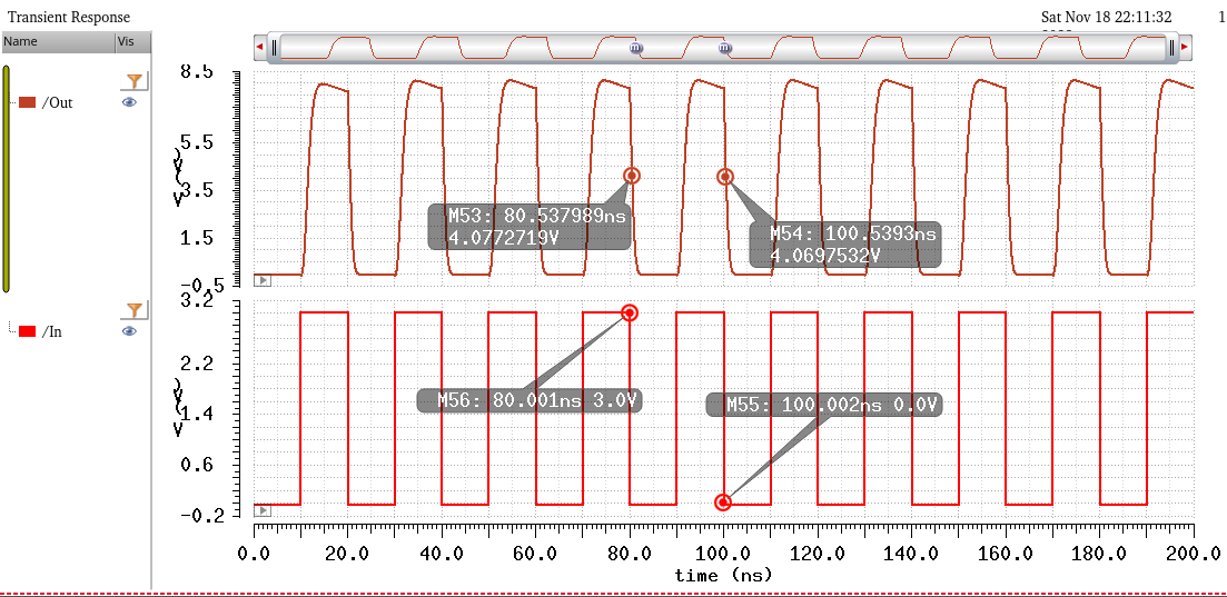
Simulating with VDD = 5V
^^^^^^^^^^^^^^^^^^^^^^^
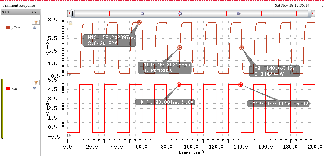
This time the output is 8V, which makes sense as a larger VDD(5V) is charging the capacitor at node B.
Tplh = 0.8ns, Tphl = 0.7ns. All design requirements are satisfied
And these are the rise and fall times:
Tr = 3.2ns, Tf = 2.1ns
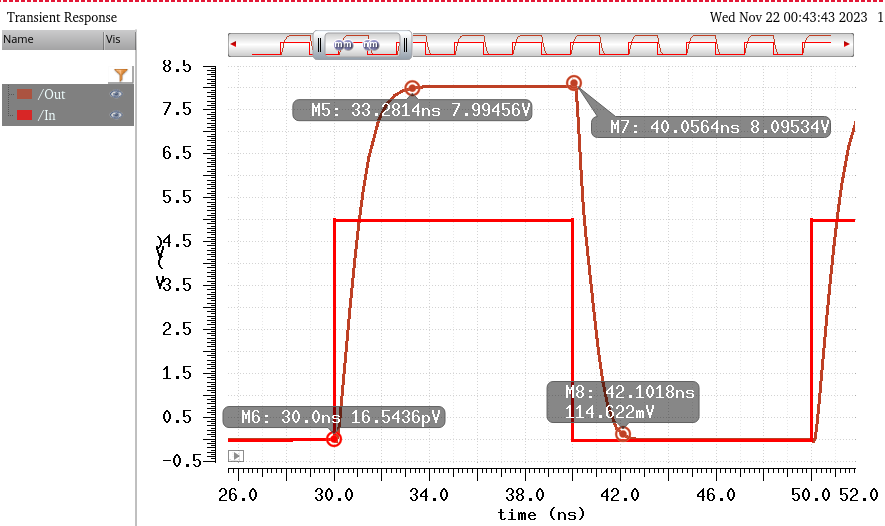
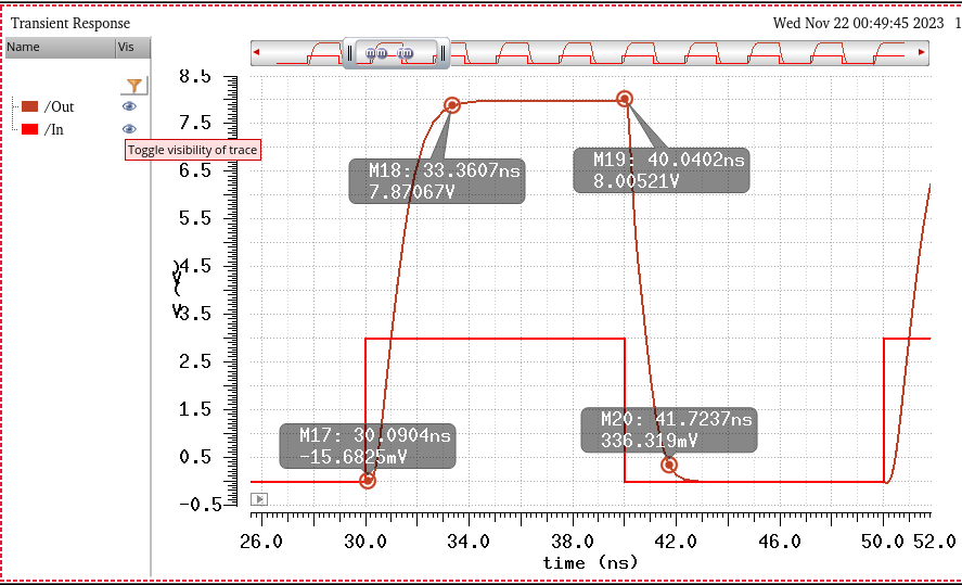
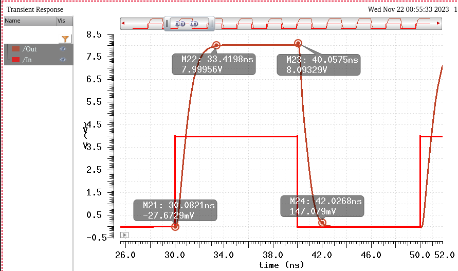
Simulating with VDD = 5.5V
^^^^^^^^^^^^^^^^^^^^^^^^^
Again, since larger VDD is charging node B capacitor, so this time the output is 8.8V.
And Tplh = 0.8ns, Tphl = 0.6ns. Design requirements are satisfied.
And here are the rise and fall times
Tr = 3ns, Tf = 2.1ns
Simulating with varying input logic
***************************************************************************************************
Based on requirements, a logic 0 is 1V or less. And a logic 1 is 3V or higher.
So I will test these values for input voltage pulses of: 0.5V, 1V, 3V, and 4V (5V was tested previously in section above).
VDD is get to 5V.
Simulating with Vin = 0.5V
^^^^^^^^^^^^^^^^^^^^^^^^
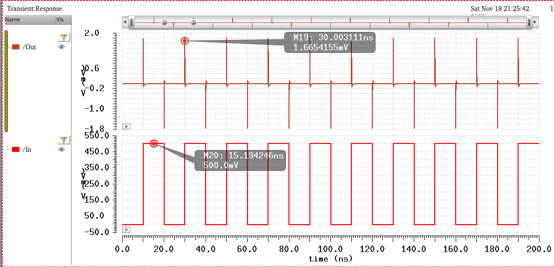
Vin = 0.5V wave is seen as input, and the output is close to 0V. As can be seen, there are some small spikes of 1.6mV, these are due to the voltage switches of the square wave, but these are a small fraction of the 500mV input, thus acting as a logic 0.
Simulating with Vin =1V
^^^^^^^^^^^^^^^^^^^^^
Again we see Vin as an alternating 1V pulse. And Vout once again has very small spikes of 3.7mV, which is it's attempt to respond to the input voltage changes. However, once again, these can be regarded as logic 0 since the output voltage is a very small fraction of 1V input.
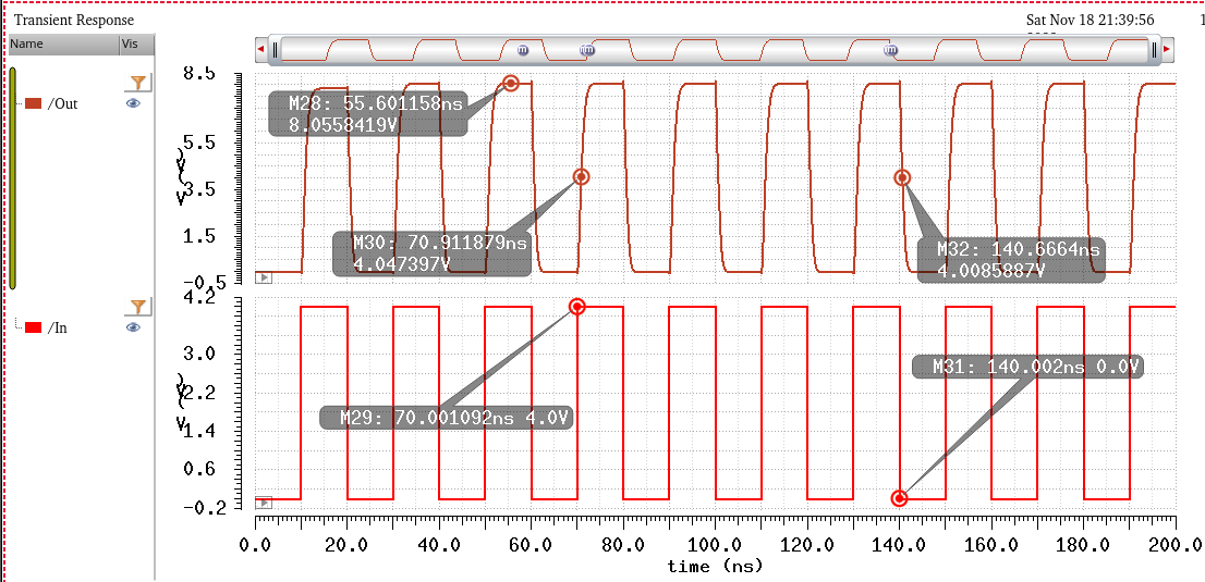
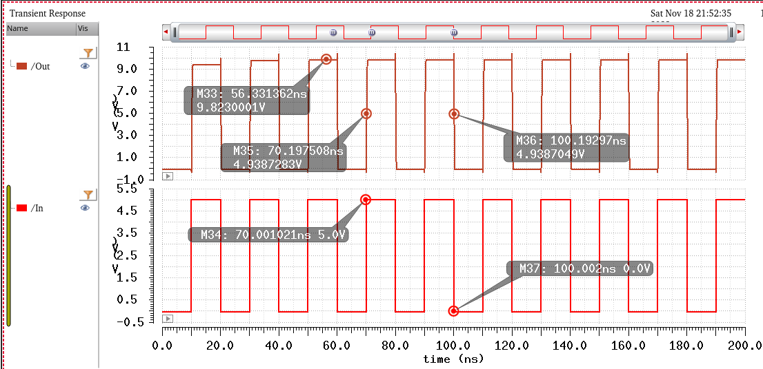
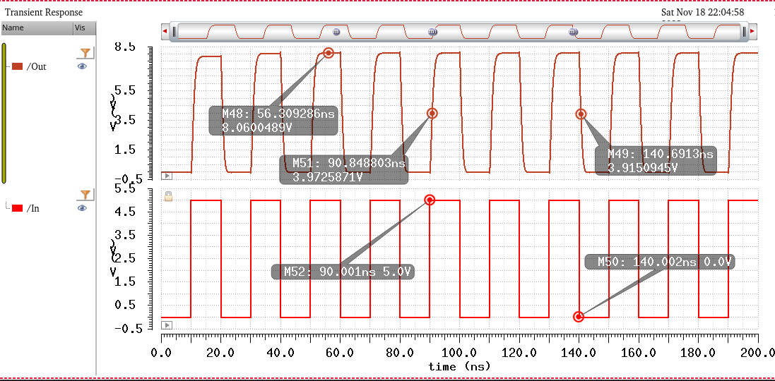
Simulating with Vin = 3V
^^^^^^^^^^^^^^^^^^^^^^
Based on design requirements, a 3V input must be a logic 1. This can be seen above. Where the input is a 3V square wave. And the output is about 8V.
Tphl = 0.6ns, and Tplh = 1.2ns. Thus all design requirements are satisfied.
And the rise/fall times....
Tr = 3.3ns, Tf = 1.7ns
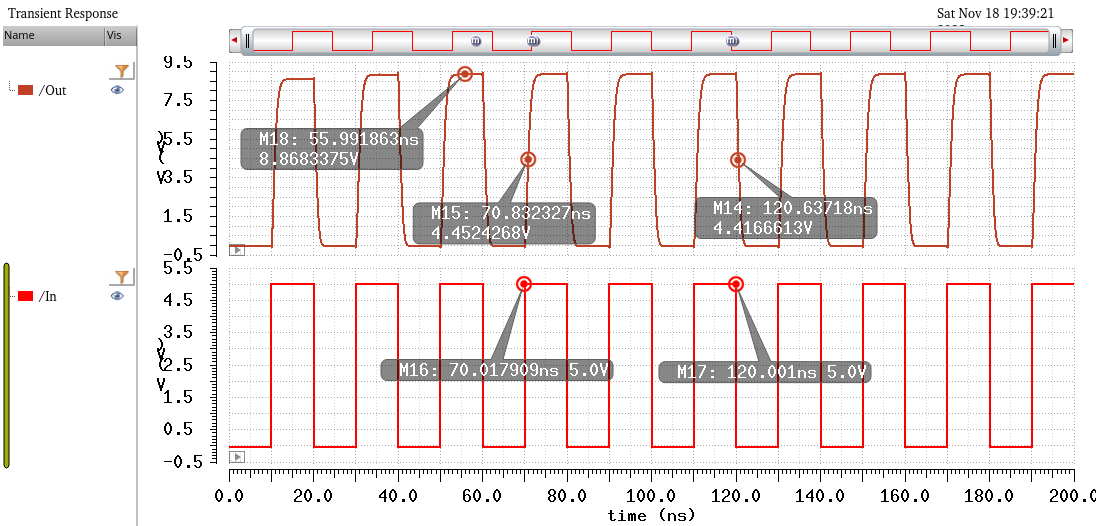
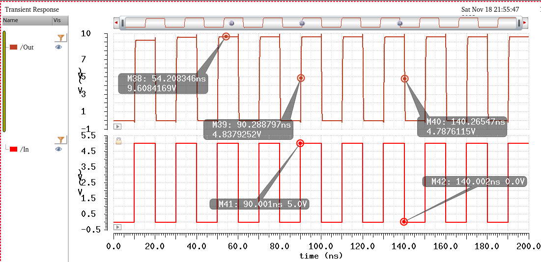
Simulating with Vin = 4V
^^^^^^^^^^^^^^^^^^^^^^
A 4V square wave input is observed. And once again, Vout = 8V.
Tphl = 0.6ns, Tplh = 0.9ns. Design requirements are satisfied. A logic 1 is observed.
And then the rise/fall times
Tr = 3.3ns, Tf = 2ns
Simulating with varying load capacitance.
***************************************************************************************************
The final design requirement is that the circuit works for any capacitances from 0 -> 1pF.
I will test the loads of 0F, 100fF, 500fF and 1pF. VDD = 5V, and an input voltage of 5V will be selected.
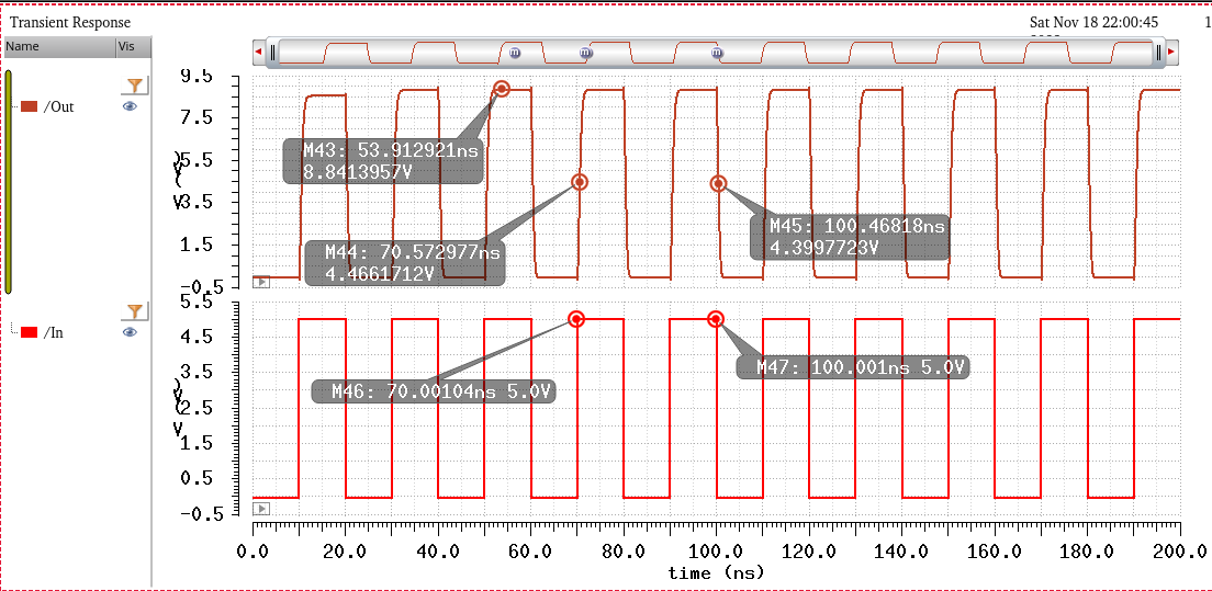
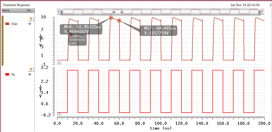
Simulating with Cload = 0F
^^^^^^^^^^^^^^^^^^^^^^^^
Vout is 9.8V, Tphl = 0.2ns, and Tplh = 2ns.
All design requirements are satisfied. The spikes of voltage are from when the input voltage is changing to 0V.
Simulating with Cload = 100fF
^^^^^^^^^^^^^^^^^^^^^^^^^^^
Vout = 9.6V, Tphl = 0.2ns, Tplh = 0.2ns
Design specifications are satisfied. The output voltage has decreased since the load now takes some charge, as compared to the previous 0F simulation.
Simulation with Cload = 500fF
^^^^^^^^^^^^^^^^^^^^^^^^^^^^
Vout = 8.8V, the continuing trend, the larger capacitors will take more charge and thus reduce the overall output voltage.
Tphl = 0.5ns, Tplh = 0.6ns, design requirements are satisfied.
Simulating with Cload = 1pF
^^^^^^^^^^^^^^^^^^^^^^^^^
Vout = 8V, Tphl = 0.7ns, Tplh = 0.8ns.
Design requirements are satisfied.
Some different simulation oddities
***************************************************************************************************
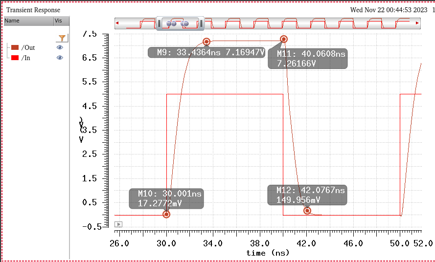
In this section, I will show a combination of inputs that provide strange waveforms.
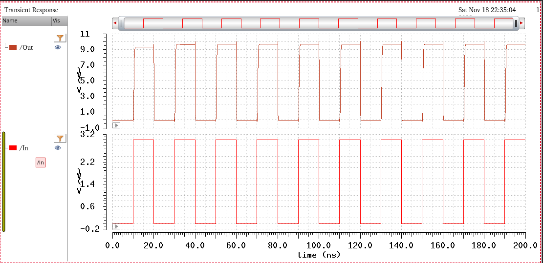
For this simulation, Cload does not matter (set to 1pF for this example), VDD = 5.5V and Vin = 3V.
And these are the results:
So as can be seen, there is a slow drop of the output voltage during logic 1. These outputs voltages still stay well above the 7V requirement. However it should be noted that the reason for this droop is because the output of INV2(roughly 3V) does not end up providing enough voltage to node B to continue to provide 2VDD for the entire duration, notice that 2VDD is briefly provided then decreases. This does not pose an issue for when a 4V input happens as it provides enough voltage to provide about 2VDD The transition times are still satisfied, and output voltage is greater than 1.
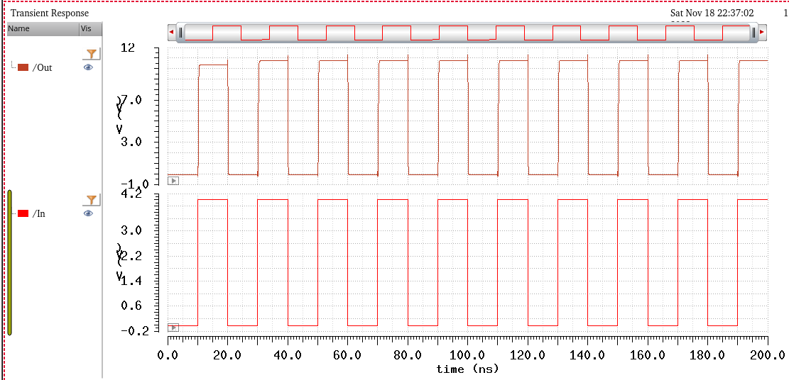
Smaller capacitances will have similar droops in logic 1, however the output voltage will still stay well above 7V, below is proof, using a 0F load. Still a 3V input and VDD = 5.5V.
***************************************************************************************************
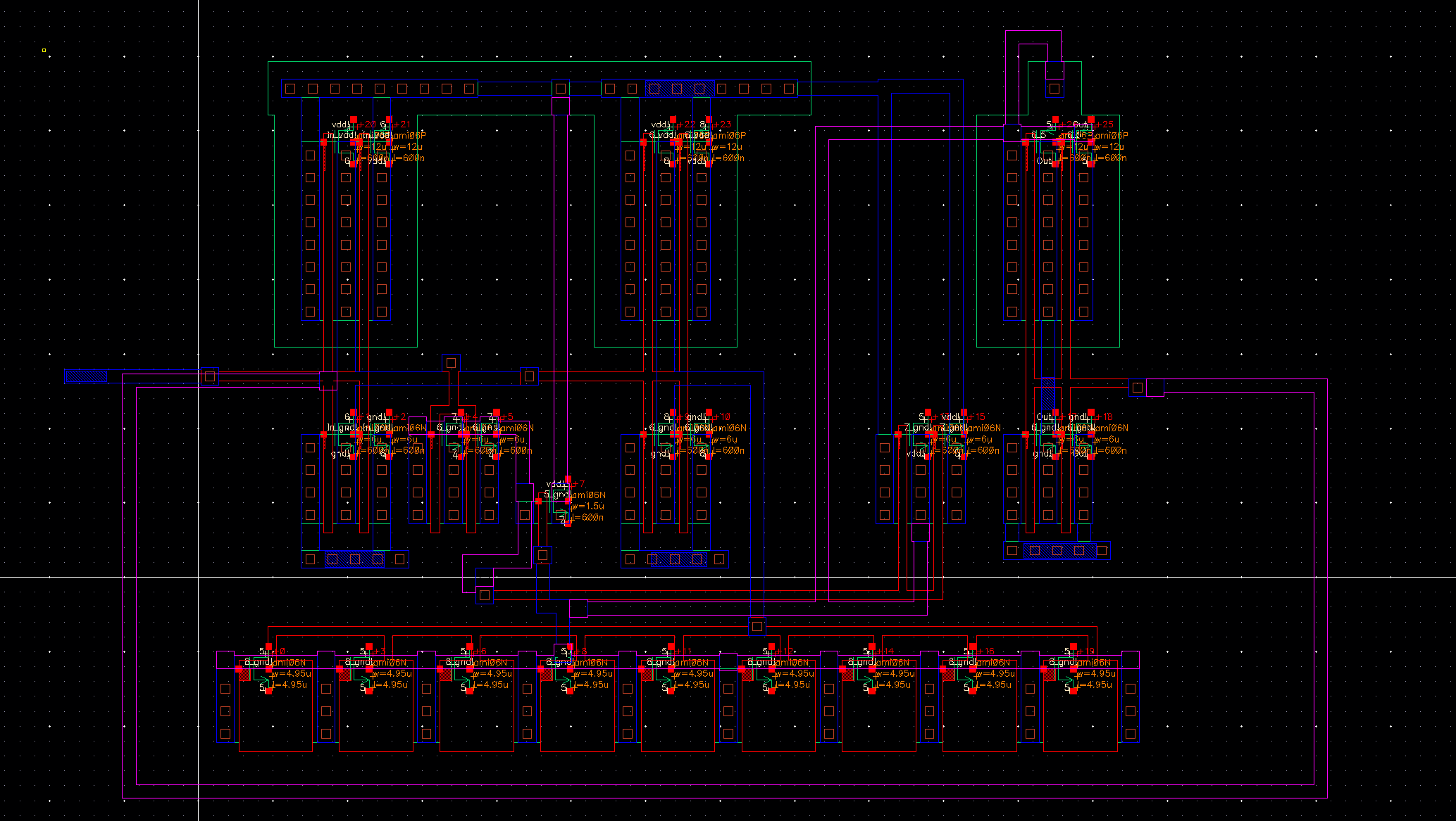
Layout: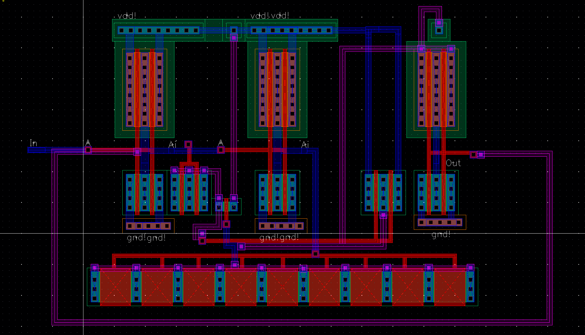 |
Extracted:
|
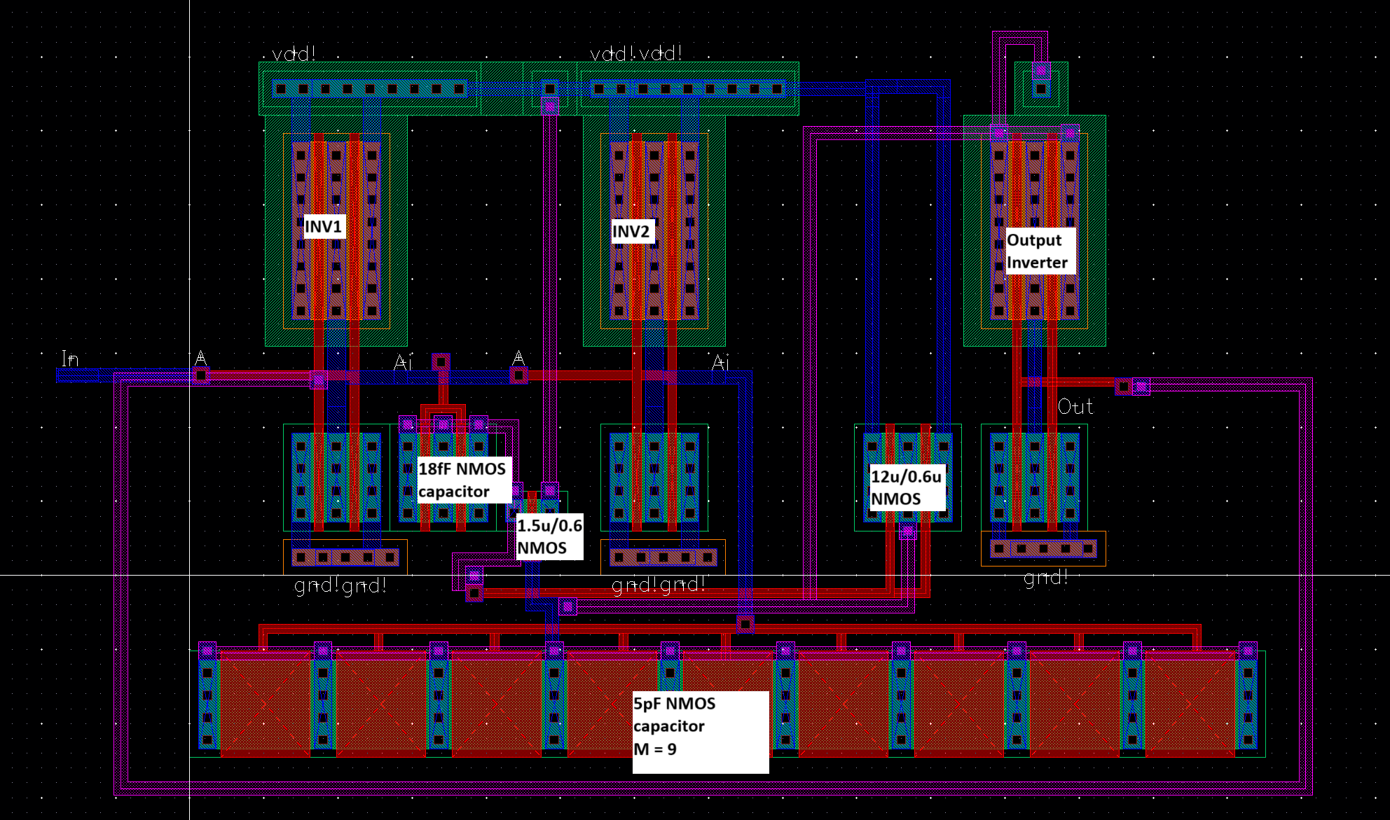
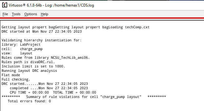
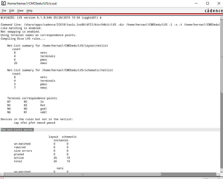
Finally DRC and LVS check, with netlists matching.
 |  |
Return to Xavier's Labs
Return to EE421 Labs