Lab 5 - ECE 421L
For this prelab, we were tasked with going through tutorial 3.
Tutorial 3 has a few questions:
1. What does the Bindkey q do?
2. Which two Cell Views are used when doing an LVS?
3. What is the difference between the nmos and nmos4 schematic cells?
4. How do you select the MOSFET models in the ADE window? What does ADE stand for?
5. What is the difference between moving and stretching?
6. How do you layout a rectangle on the metal1 layer?
7. What does the ! indicate at the end of gnd! and vdd!
8. What do the acronyms LSW and CIW stand for?
9. How is the ruler used? Cleared?
1) Edit object properties
2) Schematic and extracted
3) nmos has 3 connections, gate, source and drain. nmos4 has an additional terminal called bulk, typically going to ground.
4) In the ADE window: Setup -> Model libraries -> then follow this path: /$HOME/ncsu-cdk-1.6.0.beta/models/spectre/standalone
then you find the pmos and nmos files.
ADE stands for analoe development enviromnent.
5) Moving an object moves it. Stretching an object will either shrink or expand an object's dimensions.
6) First you must select metal1 layer, then press 'r' and draw the rectangle, then clicking again or pressing enter when you're satisfied with your shape. Alternatively you couldfind rectangle on the drop down menus and do the same drawing steps above.
7) ! means global.
8) LSW - left side window, CIW - Command interpreter window.
9) You can either find ruler in the drop down menu in Tools, or you can press 'k' to start measuring.
Then you can delete a specific ruler measurement with 'del' or you can use 'shift-k' to clear all ruler measurements.
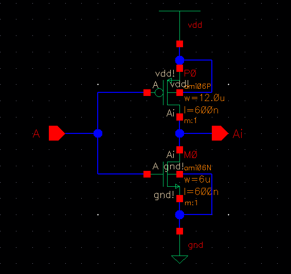
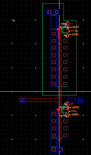
Tutorial 3 tasks us with creating a layout, symbol and schematic for a CMOS inverter.
After that the tutorial has us do a few simulations.
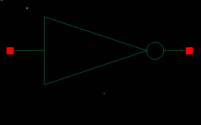
To begin, we create the inverter schematic, then we create a symbol from the schematic
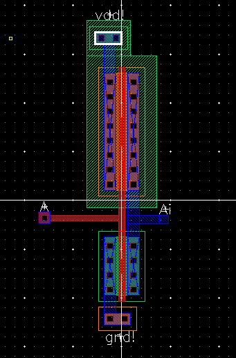
After that, we create the layout of the inverter. seen below with DRC check.
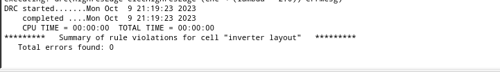
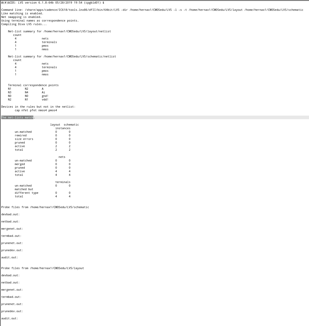
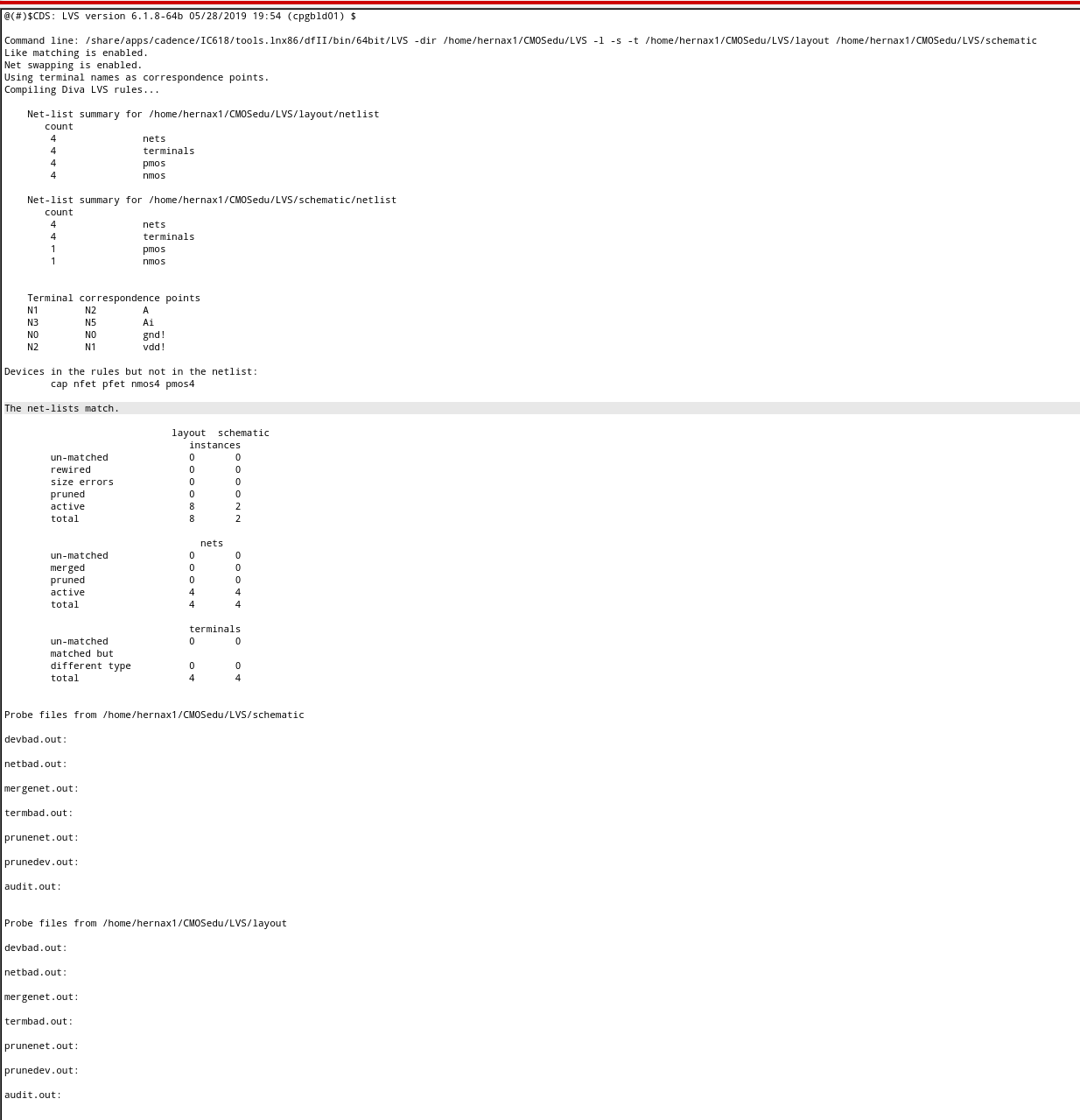
Then we extract the layout, after that we LVS our layout and the netlists match.
Now that our schematic, symbol and layout have all been completed. We can do simulations to see our inverter's operation.
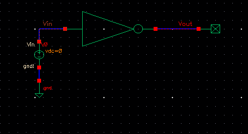
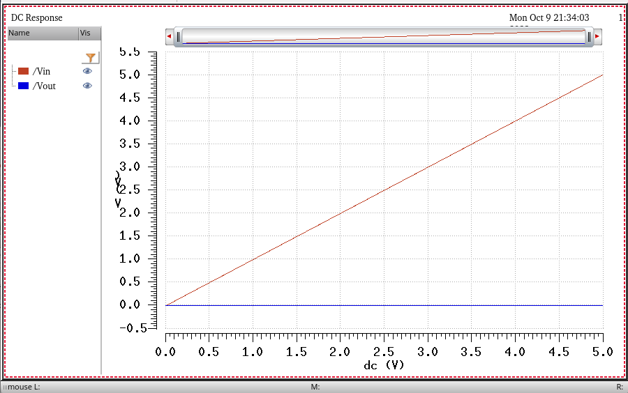
For the first simulations, we use this schematic below.
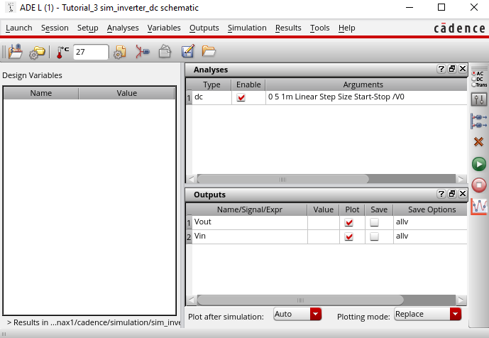
With these settings.
Which then gives us these simulation results.
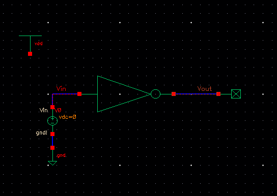
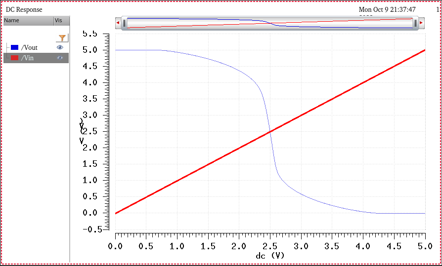
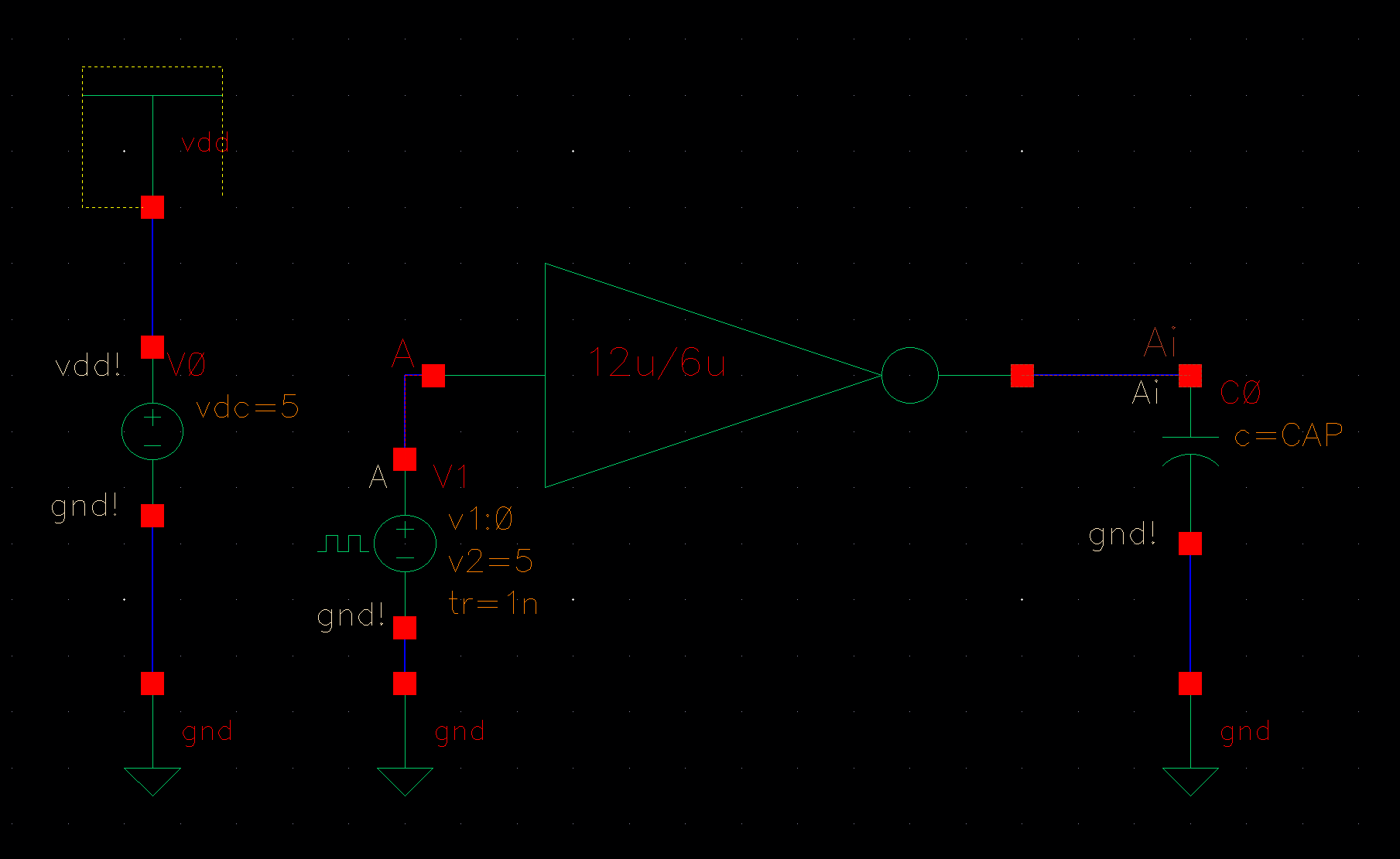
Next we are tasked with simulating this schematic. Inclusion of Vdd. Simulations done using schematic inverter
After setting up a Stimuli, we get these simulation results
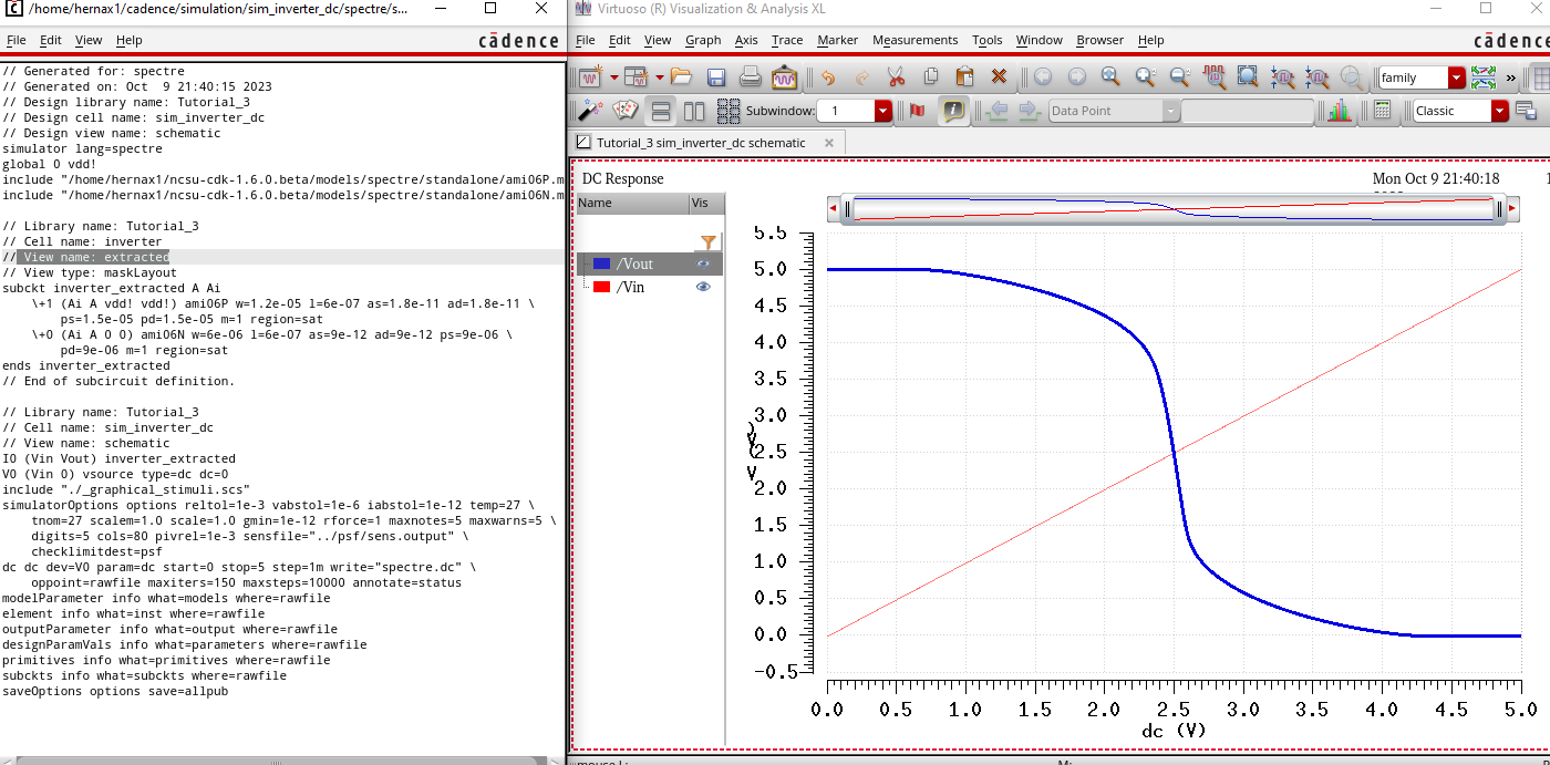
Finally, we want to simulate the same schematic but this time simulating with our extracted layout.
Seen below with proof that simulation was completed using extracted, and we get the same exact results, which is as expected since our inverter was an LVS match.
Lab Work
Draft schematics, layouts, and symbols for two inverters
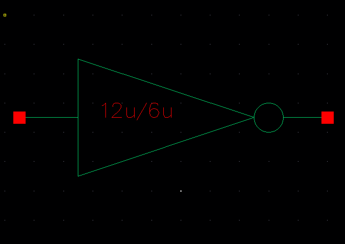
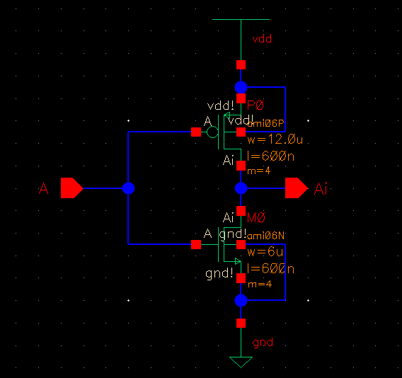
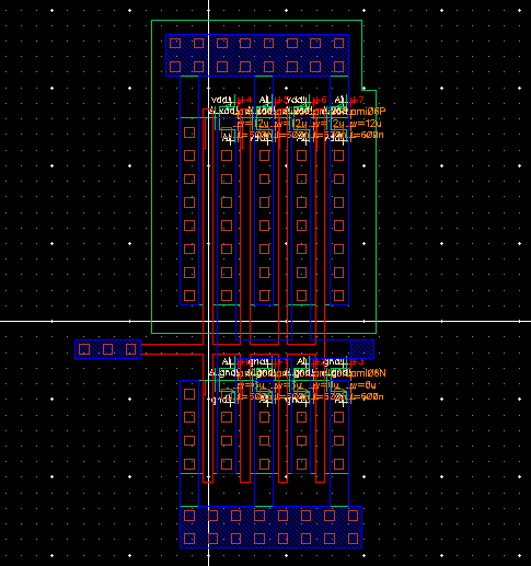
12u/6u Inverter
Schematic of inverter, and corresponding symbol.
Layout of inverter and it passing DRC check:
Extracted layout and LVS check with netlists matching.
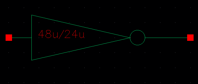
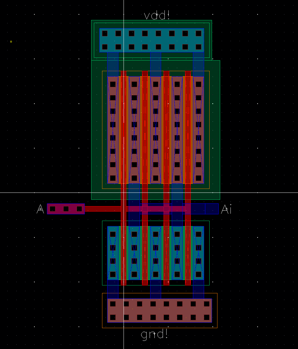
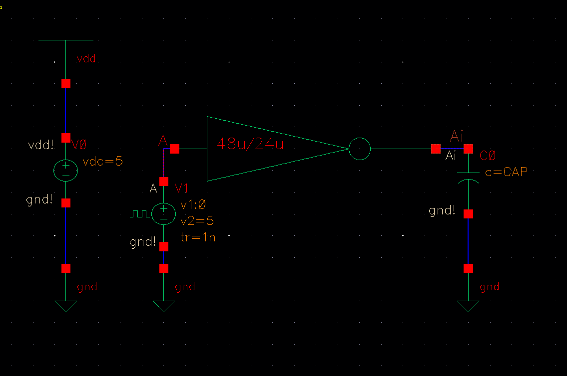
48u/24u Inverter
Schematic of inverter, using multiplier of 4. Corresponding symbol.
Layout of inverter and DRC check.

Extracted layout and LVS check, netlists match.
12u/6u simulations
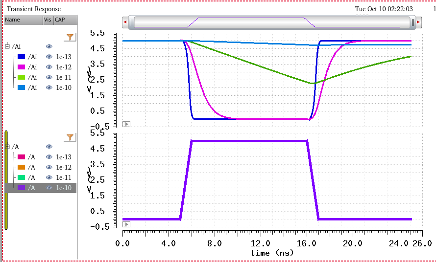
Then we simulate, with the capacitor being 100fF, 1pF, 10pF, and 100pF.
To make this simpler/easier, we can vary the capacitance using parametric analysis.
We end up with these results.:
Spectre Simulation:
Ultrasim Simulation
Clearly we can see the the smallest capacitor of 100fF provided the best curve output that behaved most like an inverter, near instataneous response. Bigger capacitance values have a clear delay with them becoming inverted.
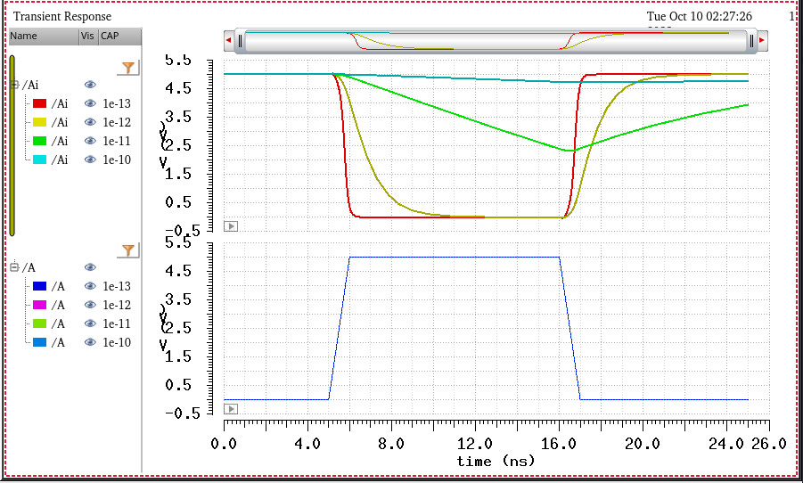
48u/24u Simulations
We do the same analysis simulations but BUT we switch out our invertor for the one with 4 fingers (multiplier). Schamtic below:
Spectre simulations
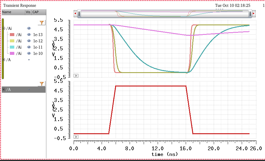
Ultrasim simulations:
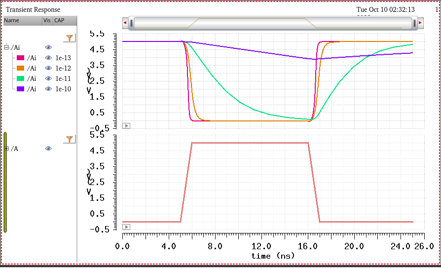
Clearly we again see that the capacitance value of 100fF provided the best output that has near instantenous inversion. In fact, the next highest capacitor, 1pF also ends up having close to no delay on inversion. Higher capacitor values still have large delays.
So as we observed in simulations, the 48u/24u inverter proved to be better than the 12u/6u inverter by allowing larger capacitor values to have almost time delay free inversion. We further know that this is caused by the multiplier, 4 in this case. Those additional branches allow for the capacitor to more effcienctly charge and discharge. The 12u/6u MOSFET is limited to one path, multiplier = 1, so that causes the capacitor to only have one path to charge/discharge, making it slower relative to the 48u/24u MOSFET.
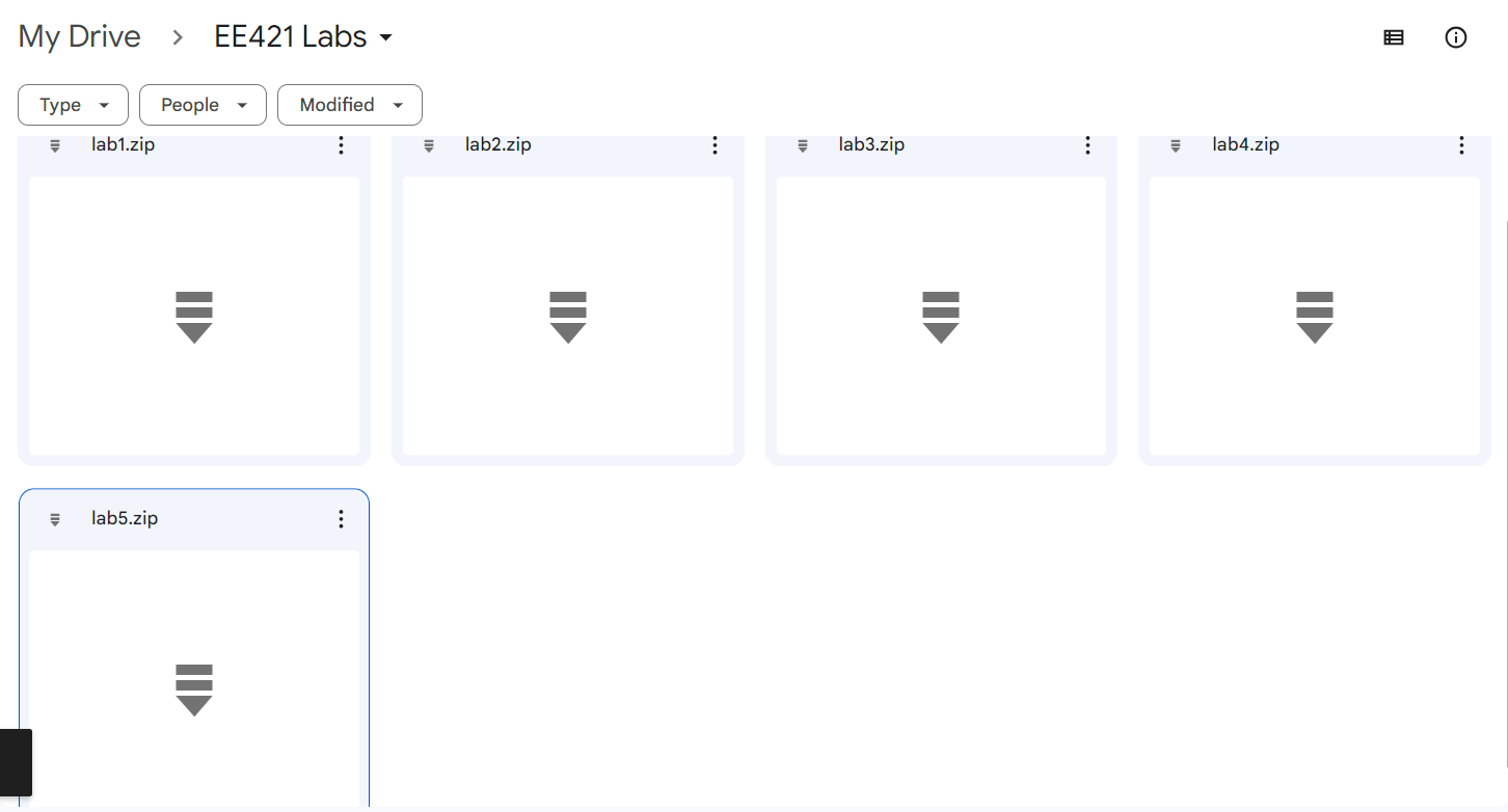
The lab files for this lab can be found here.
Included are my inverter layouts,schematic,and extracted, as well as my simulation schematic.
Lab files getting backed up
Return to Xavier's Labs
Return to EE421 Labs