Project - EE 421L
Design a non-inverting buffer circuit that presents less than 100 fF input capacitance to on-chip logic and that can drive up to a 1 pF load with output voltages greater than 7V (an output logic 0 is near ground and an output logic 1 is greater than 7V). Assume VDD is between 4.5V and 5.5V, a valid input logic 0 is 1V or less, a valid input logic 1 is 3V or more. Show that your design works with varying load capacitance from 0 to 1pF. Assume the slowest transition time allowed is 4 ns.
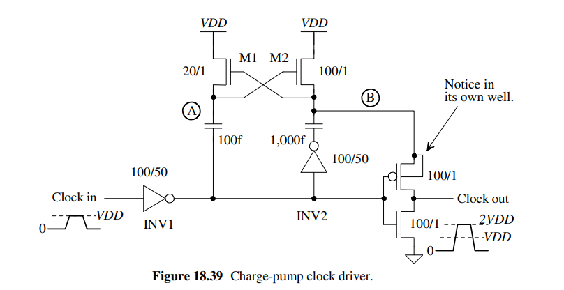
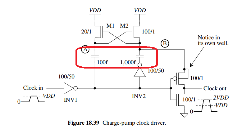
Figure Referenced For Design
For this design, we will be referencing Figure 18.39 from our CMOS text book using C5 process. We'll be referencing this primarily becuase it is similar to our design specifications, the output is non-inverting and most importantly it allows us to output 2vdd. We will design the inverters, MOSFETs and capacitors to fit our specification requirements.
Input Capacitance
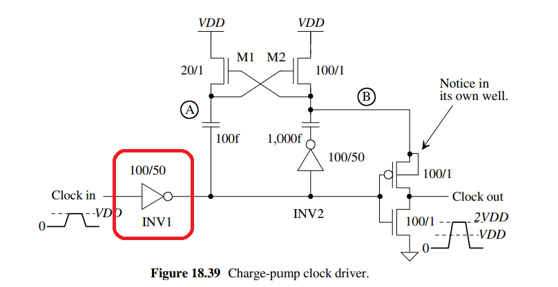
The input capacitance we know will only come from INV1. So our input capacitance for this non-inverting buffer can be calculated as shown below:
Cin = CinP + CinN
where,
From here, we know that for C5 process the drawn length is L = LP = LN = 0.6um and Cox'= 2.5fF/um^2. To limit our input capacitance, we can then set Cin equal to our allowed value, 100fF.
Cin = 100fF = (3/2)Cox'(WPLP + WNLN)
= (3/2)Cox'L(WP + WN)
To make the PMOS and NMOS have the same resitance we must make 2WN = WP. This then yields:
Cin = 100fF = (3/2)Cox'L(3WN)
100fF= (9/2)Cox'LWN
WN = [ (100fF)(2) ] / [ 9Cox'L ] ~ 12um
So for the first inverter, INV1, to achieve an input capacitance less than 100fF, WN = 12um and WP = 24um. In summary, we have a 24/12 Inverter.
Sizing Last Inverter for Delay < 4ns
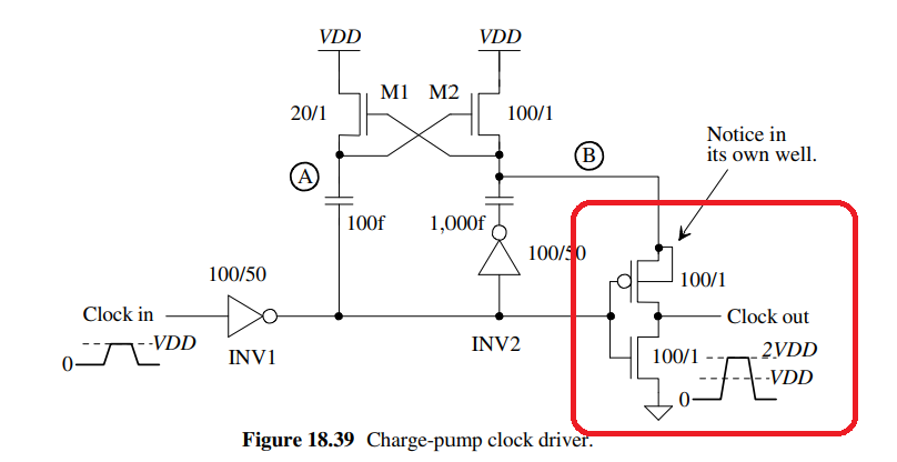
To achieve a proper transition time below 4ns, we need to size the right-most MOSFETS shown above, appropiatley. We know that for a propagation delay time whether high-to-low, tPHL, or low-to-high, tPLH, we can consider the equation:
tPHL = tPLH = 0.7RCload
Where Cload, is the load capacitance, and R is the resistance of our MOSFET's. Since we want our design to have a transistion time below 4ns, we will set our delay time to about 1ns. Solving the equation, with the worst case scenario of Cload = 1pF, yields the following:
R = 1ns / (0.7*Cload ) ~ 1k
Estemating the rise and fall times of our outputs:
tLH = tHL = 2.2*R*Cload= 2.2*1k*1pF = 2.2ns
We then size our inverters MOSFET's to have this resitance (i.e R = 1k). The resistance can be calculated by the following equation. For now we'll solve for the the width of our NMOS:
RN = RN'*LN/WN
Where in our C5 process:
Solving for WN, we get about 12 um. Similarly for the PMOS, result yields WP = 24 um.
It is also important to note that the bulk of the PMOS is connected to its own well so that we keep the source terminal always at the same potential as the body, to avoid any body effect and unwanted behavior of the PMOS.
In summary, we have a 24u/.6u PMOS and a 12u/.6u NMOS.
INV2
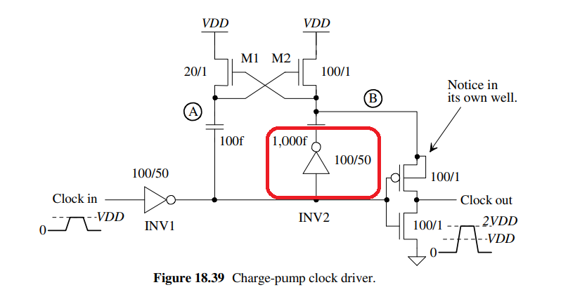
Inverter 2 will be similar to INV1 for simplicity. We want both propagation delays tPLH and tPHL to be similar and since its used to boost node B up to 2vdd, this will suffice for the designs purpose.
Sizing Capacitor to charge Cload (Using an NMOS)
Assuming for now that we will be using a capacitor for the schematic, we need to size the right-most capacitor so that its big enough to supply charge to the load. When the PMOS turns on in our last inverter, we can simplify both capacitors as if they are charge sharing. Thus, we can simplify to the following:
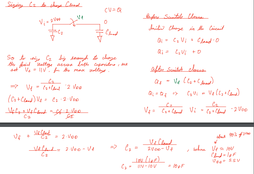
As seen in the hald calculations above, we will require a capacitor of about 10pF. Now since we are using a MOSFET in strong inversion, NMOS in our case, we need to use the 10pF calculated as our Cox and find the width and length for the NMOS. We will set the width and length to be equal to each other so that we can simplify the derivation as seen below:
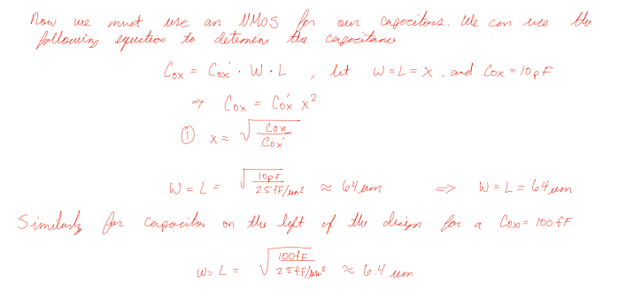
For the NMOS that will be used as a capacitor to charge the load, will have both width and length equal to 64um. For the other capacitor that will simply be used to turn on
M2, will have a width and length equal to 6.4um.
M1 and M2
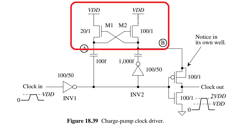
M1 is sized smaller than M2 to reduce layout area and power. M2 will be sized bigger so that its able to pull node B up to vdd quicker, since it will have a lower resitance. So in my design, M2 will be 60u/.6u and M1 will be 12u/.6u.
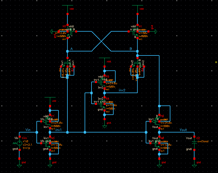
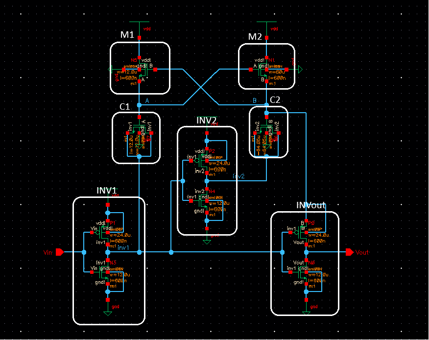
Non-Inverting Buffer
Putting everything together into the schematic we get the following:
Simulations
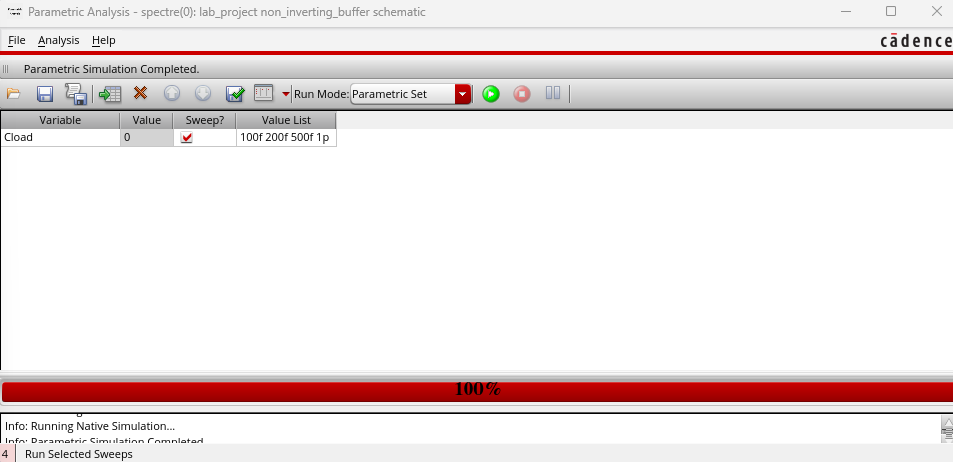
In the following simulations, I will vary the load capacitance from 100fF,200fF, 500fF and 1pF using a parametric analysis to save time on simulations.
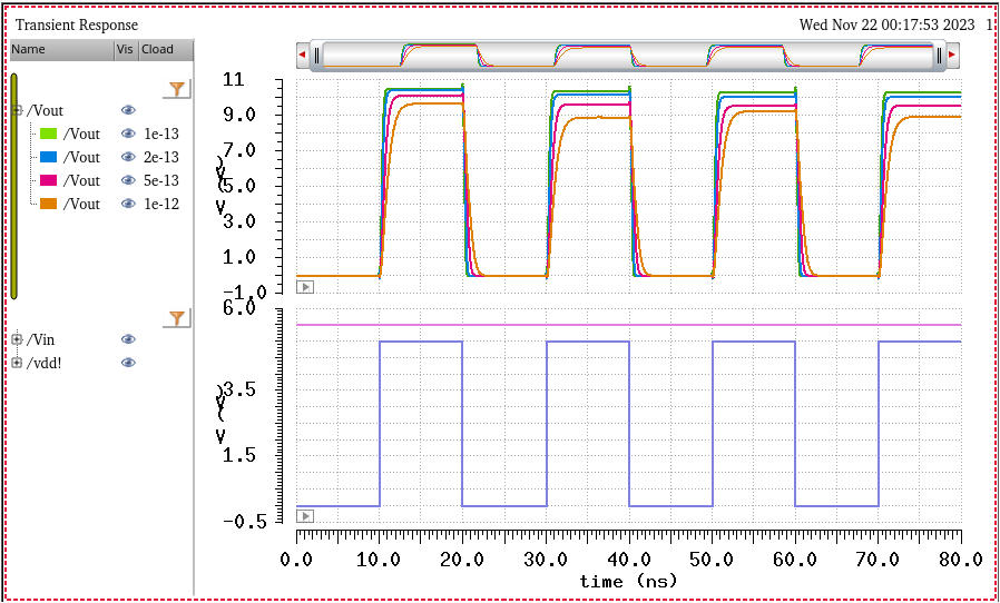
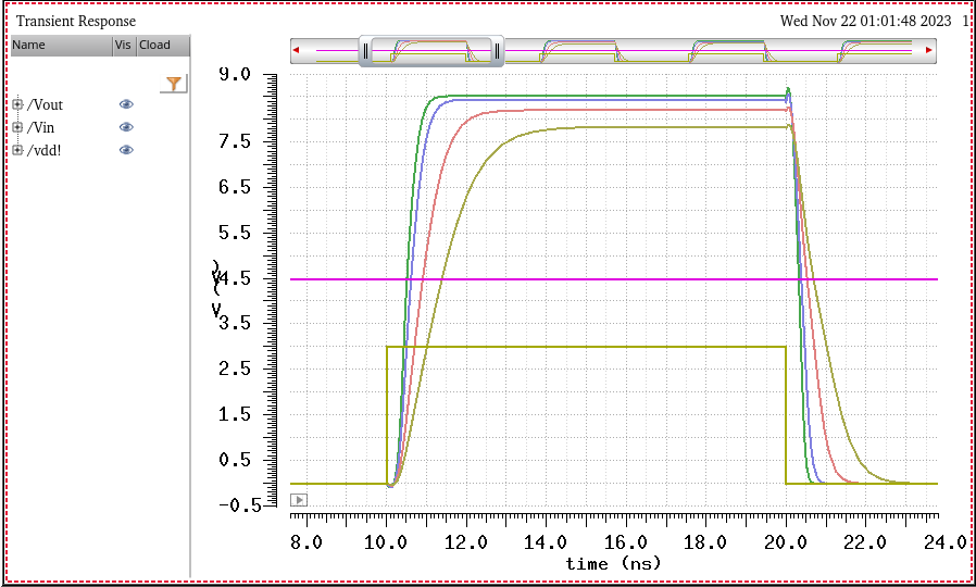
1. For starters, we wil test the scheamtic with vdd at 5V with varrying loads.
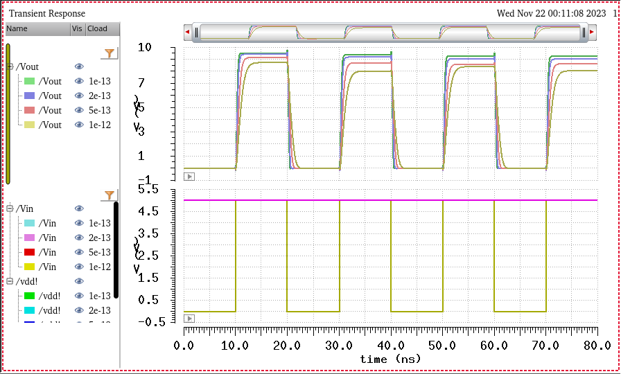
As seen above, the results yield a logic 1 (Vin above 3V), is well above 7V when vdd = 5V.
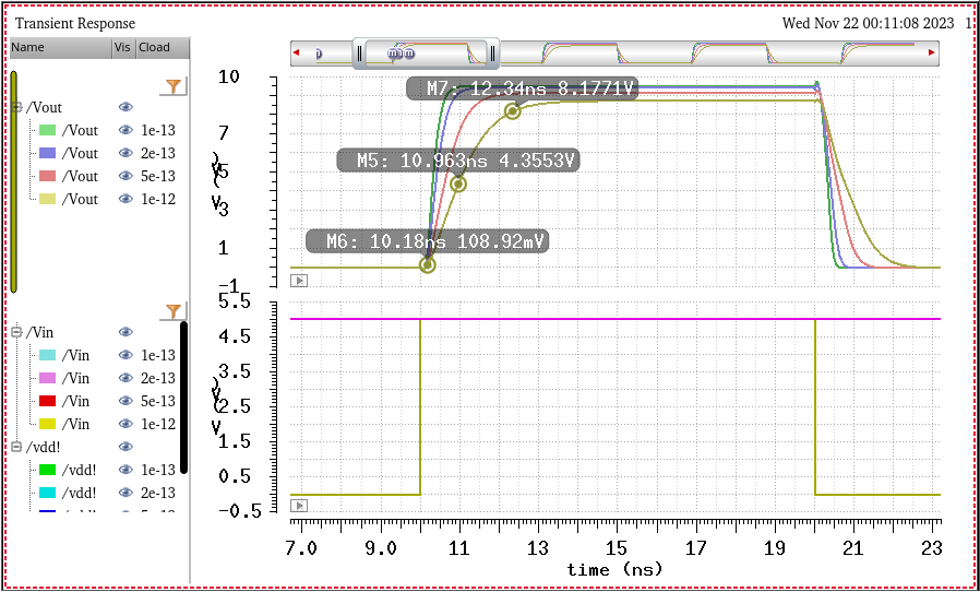
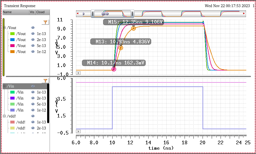
Observing our time delay in our ouput above, we see that after the pulse comes on at 10ns, after about 1ns, our propagation high-to-low is as expected from the hand calculations. The result is not exact, but it is in a acceptable range. The transition time tLH and tHL are approximatley 2.3ns close to our expected value. The other loads are similar so for simplicity we will just analyze the 1pF load.
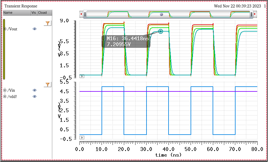
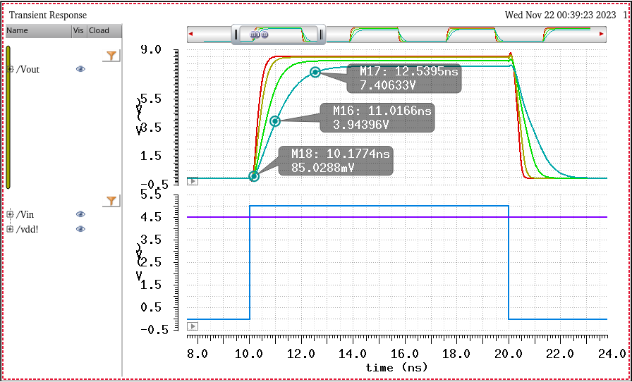
2. Now I will change vdd up to 5.5V while still keeping Vin oscillating to 5V.
The results are similar to the previous test. Vdd is at 5.5V and our ouptut is still above 7V.
We can notice the output shifted higher then the previous results. Time delays and transistions times are still failry similar.
3. Now we test below 5V, that is vdd at 4.5V. Results are shown below.
You can see that at the lowest case we still have the output voltage above 7V. Below you can also confirm that the time delay and transisition times are also similar to previous tests.
Finally, we will test the input voltage to make sure we get logic 1 for 3V or higher, or logic 0 for less than 1V. Note that I kept vdd at 4.5V to make sure that even with the input voltage changing, results will remain the same at worst case scenario.
4. Changing Vin to 1V, we can confirm below that we get a logic 0.
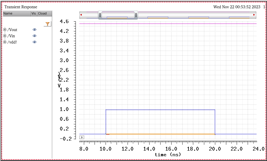
5. Changing Vin to 3V, below you can verify that we get a logic 1.
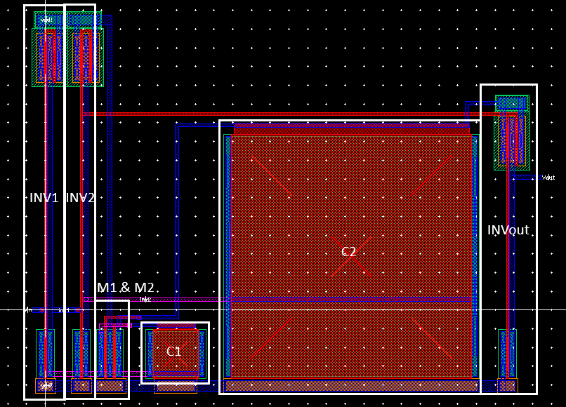
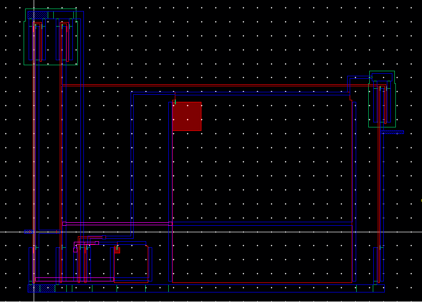
Layout
In the schematic above, in order to obtain a clean LVS, a small change had to be made. For the two NMOS that are being used as capacitors, we must tie the body to ground since our p-substrate is already tied to ground by other MOSFETS. When doing so, I had to increase the size of left capacitor to keep any major drawbacks on the output simulations. The final schematic that I will layout is below.
Respective layout and extracted view:
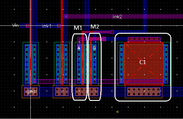
Lower Left Area Zoomed in:
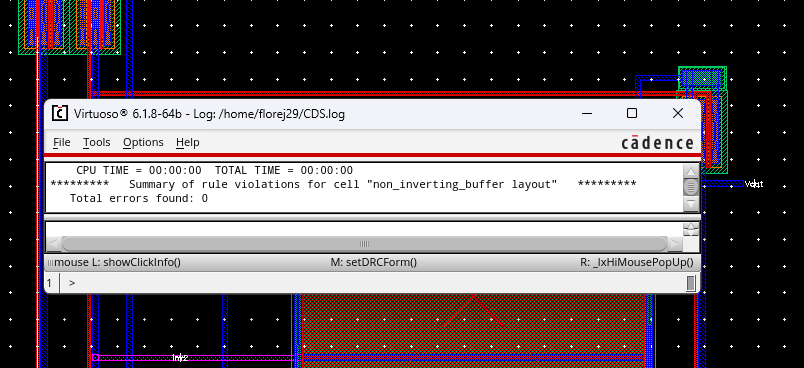
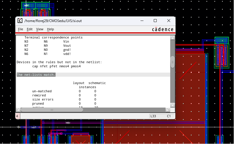
Clean DRC and LVS:
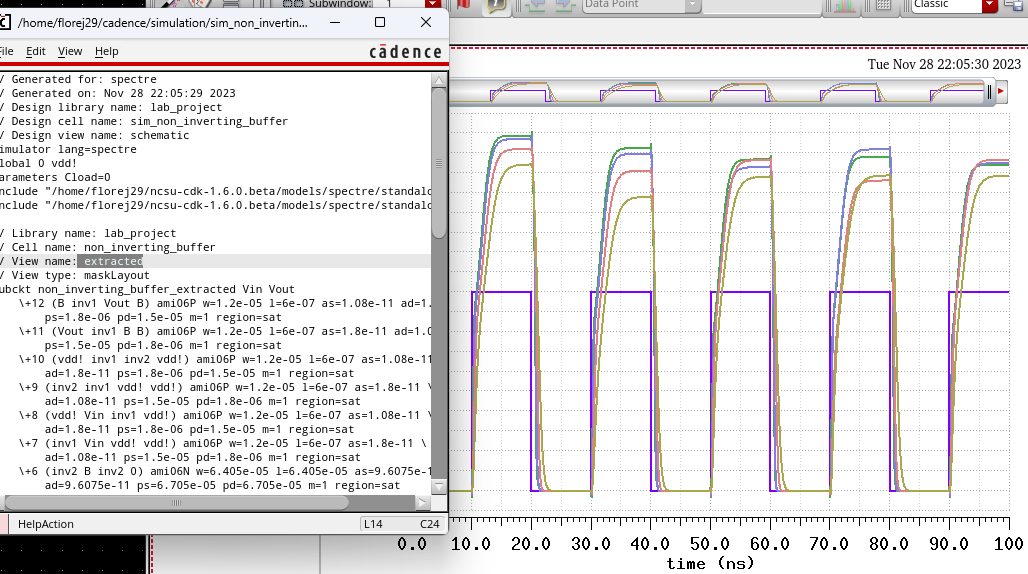
Lastly, we can simulate the extracted layout.
Below is my zipped up files for this project.
>> project <<