Lab 7 - EE 421L
Using
buses and arrays in the design of word inverters, muxes, and high-speed
adders.
Lab Objectives
Provide a few simulation examples using these gates.
-
2-to-1
DEMUX/MUX (and the symbol).
Simulate the operation of this circuit
using Spectre and explain how it works.
Make sure to show, using simulations, how the circuit can be used for both multiplexing and de-multiplexing.
- Create
an 8-bit wide word 2-to-1 DEMUX/MUX schematic and symbol.
Include
an inverter in your design so the cell only needs one select input, S
(the complement, Si, is generated using an inverter).
Use
simulations to verify the operation of your design.
-
Draft
the schematic of the full-adder seen in Fig. 12.20 using 6u/0.6u
devices (both PMOS and NMOS).
Create an adder symbol for this circuit (see the symbol used in lab6).
Lab
4-bit input/output Inverter
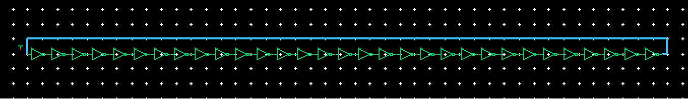
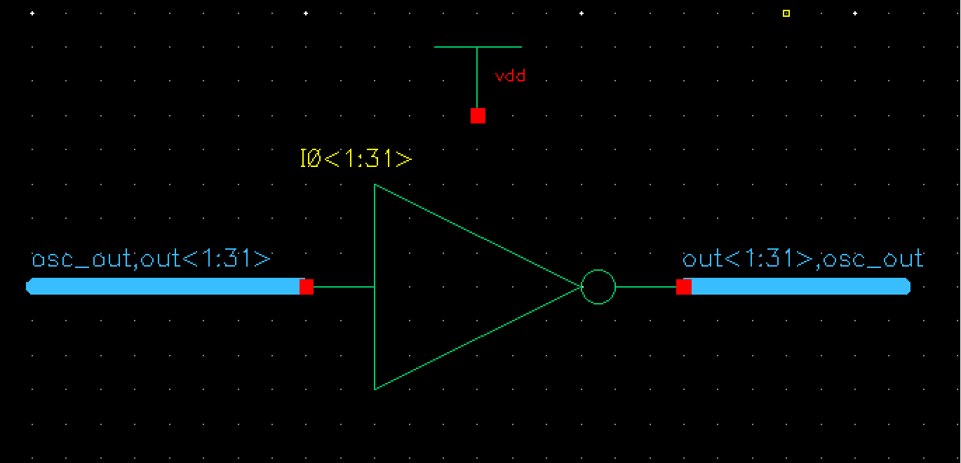
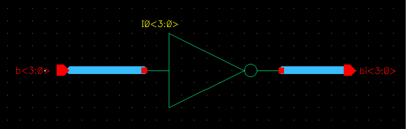
For this 4-input inverter, we repoeat the same process as we did in the pre-lab, but instead we only need 4 wire bus as seen below.
The symbol is then created:
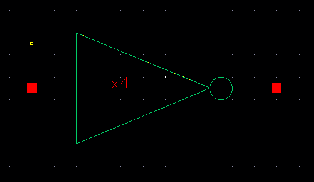
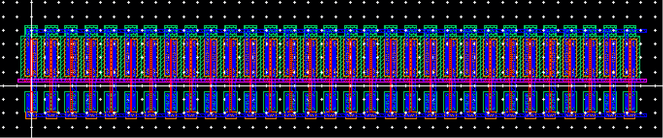
Now that we have our symbol created, we can then proceed to drawing the schematic per the lab report. See below:
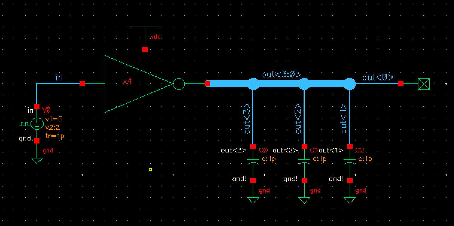
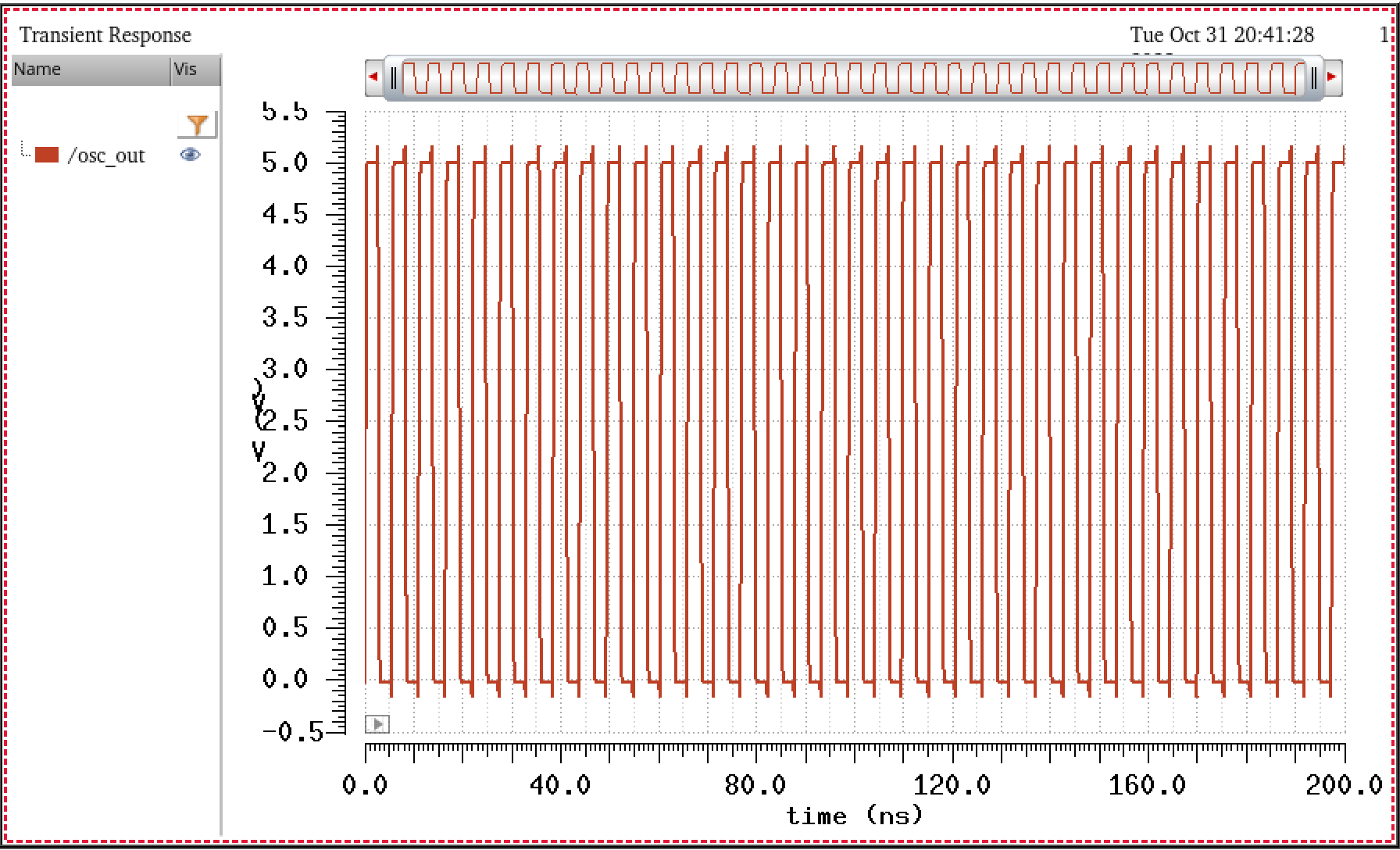
After setting up our simulation settings, the results are seen below:
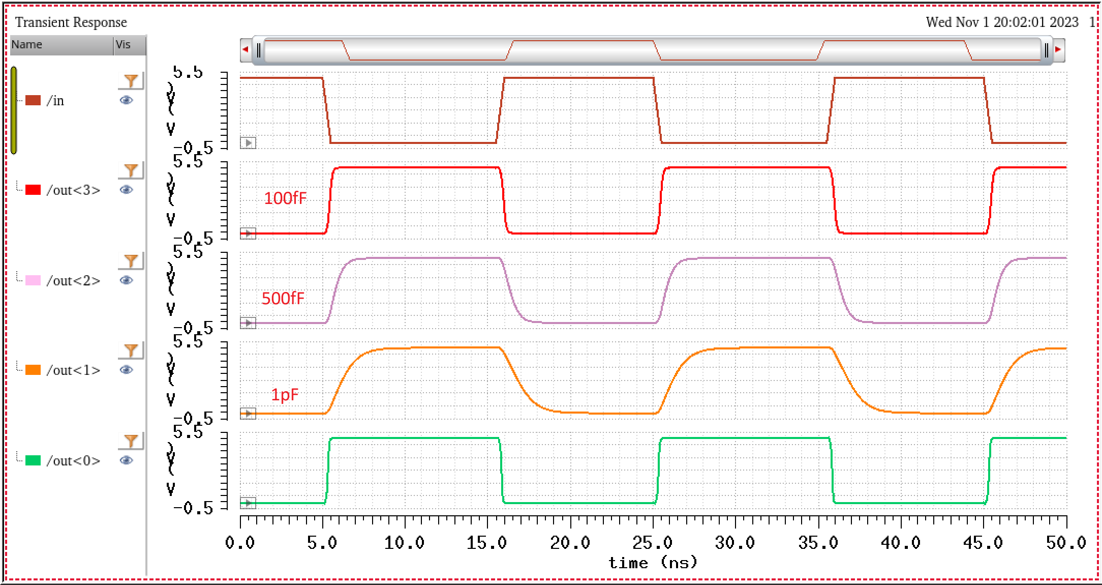
As seen from the results above, we can conclude that the size of the size of the capacitors effects how fast the outputs are charged or discharged to their respective value. Analyzing the plots, we see that the 100fF capacitive load lets our ouput rise or drop quicker compared to the 500, 1 pF capacitors. As we increase the capacitance, the rise/fall times or slower.
8-bit input/output NAND Gate
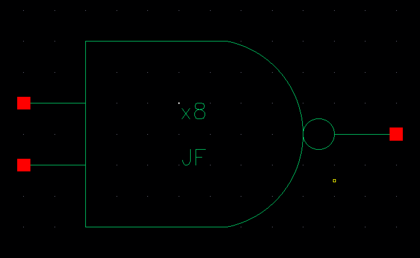
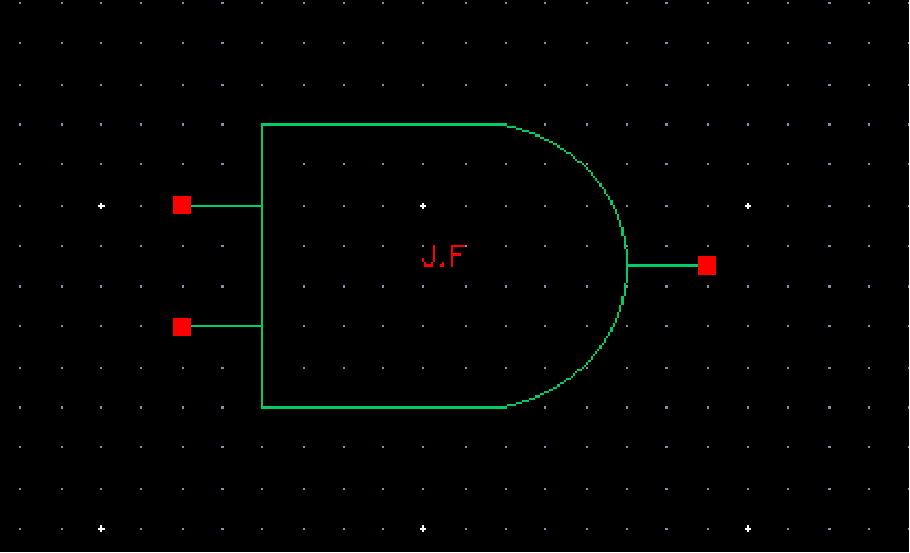
For this 8-bit input/output NAND gate, we can follow similar procedures as we did with the inverter. We instantiate the NAND gate we've previously done in other labs, and make an array of 8, and also connect 8-bit wide wires to each input and output so that we have something similar to what was shown in the lab report. We get the following:
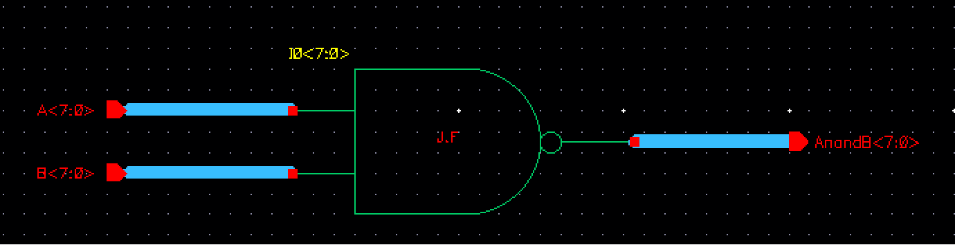
This symbol for this schematic is then:
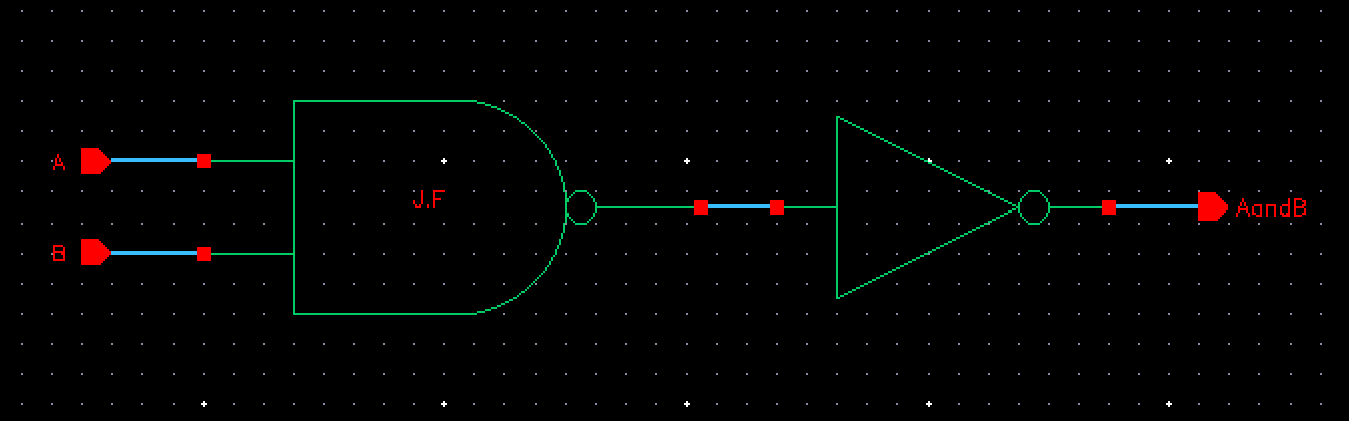
8-bit input/output AND Gate
Following the NAND gate we can create the AND gate by simply placing an inverter infront it as shown below:
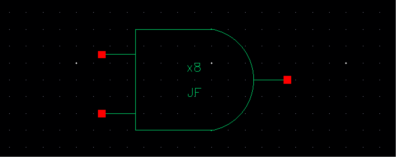
We can then create the symbol:
Now that we have our AND gate, we can now create the 8-bit input/output AND gate:
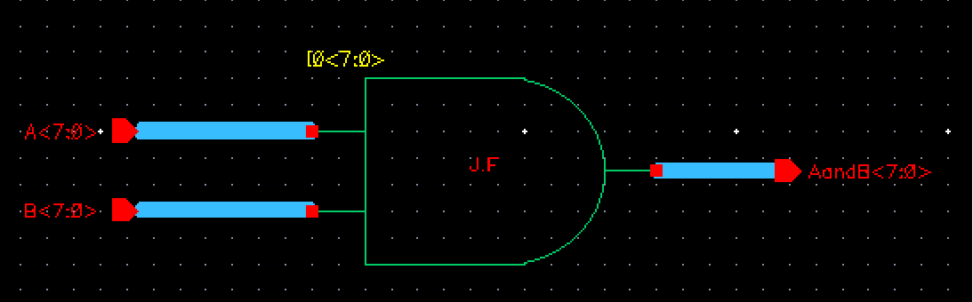
The symbol is then:
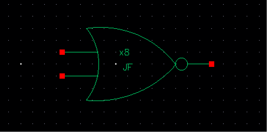
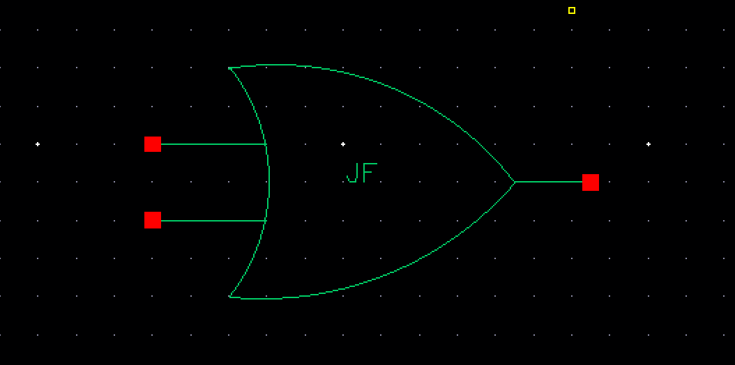
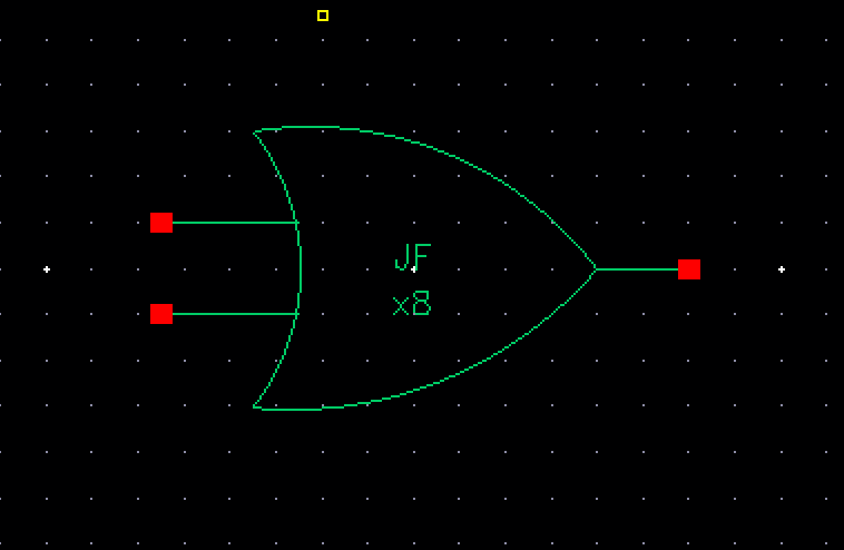
8-bit input/output NOR Gate
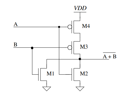
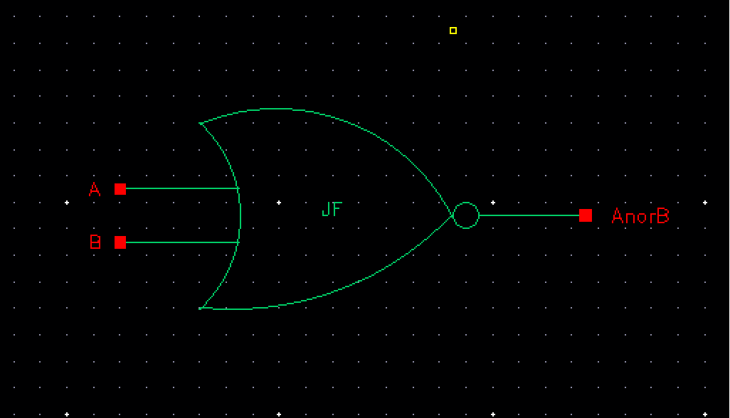
We need to create a 2-input NOR Gate, in order to then use it for a 8-bit input/outputs. To begin, we can start by drawing out the schematic of a NOR gate as seen in our CMOS book on page 370, Chapter 12, Figure 12.1.
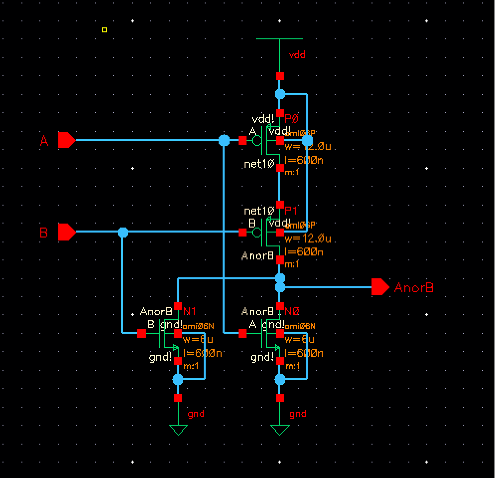
Creating the symbol for this NOR gate schematic:
To confirm the operation of the 2-input NOR gate, we will simulate it to make sure we get expected values. Below you can see the truth table in sequential order for the NOR gate.
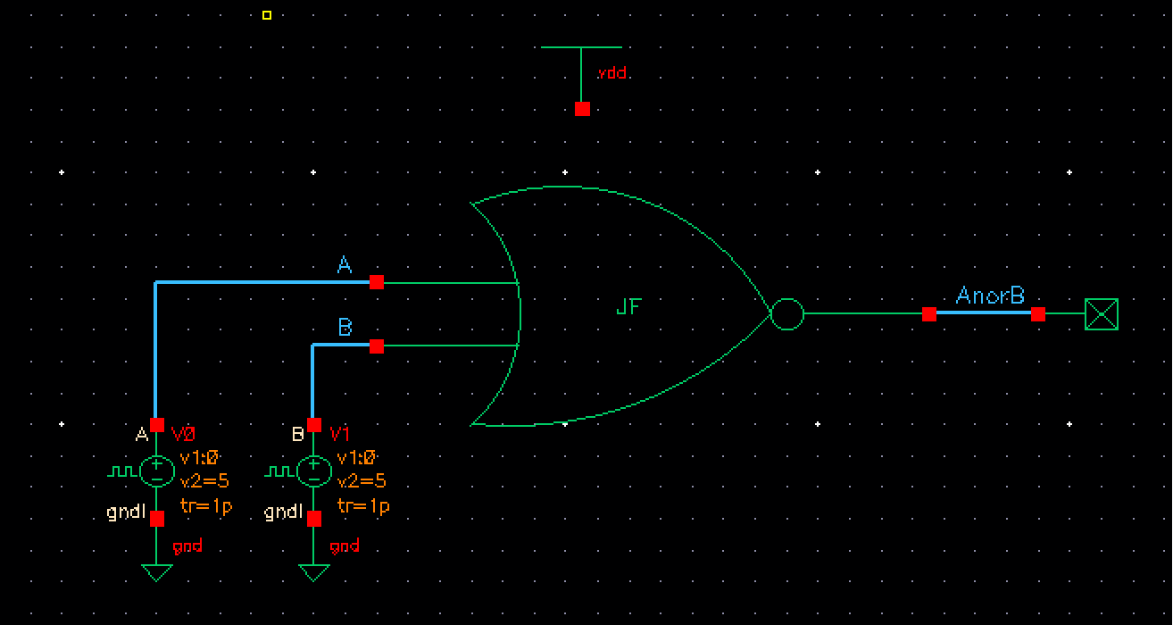
NOR Gate Truth Table
| A | B | AnorB |
| 0 | 0 | 1 |
| 0 | 1 | 0 |
| 1 | 0 | 0 |
| 1 | 1 | 0 |
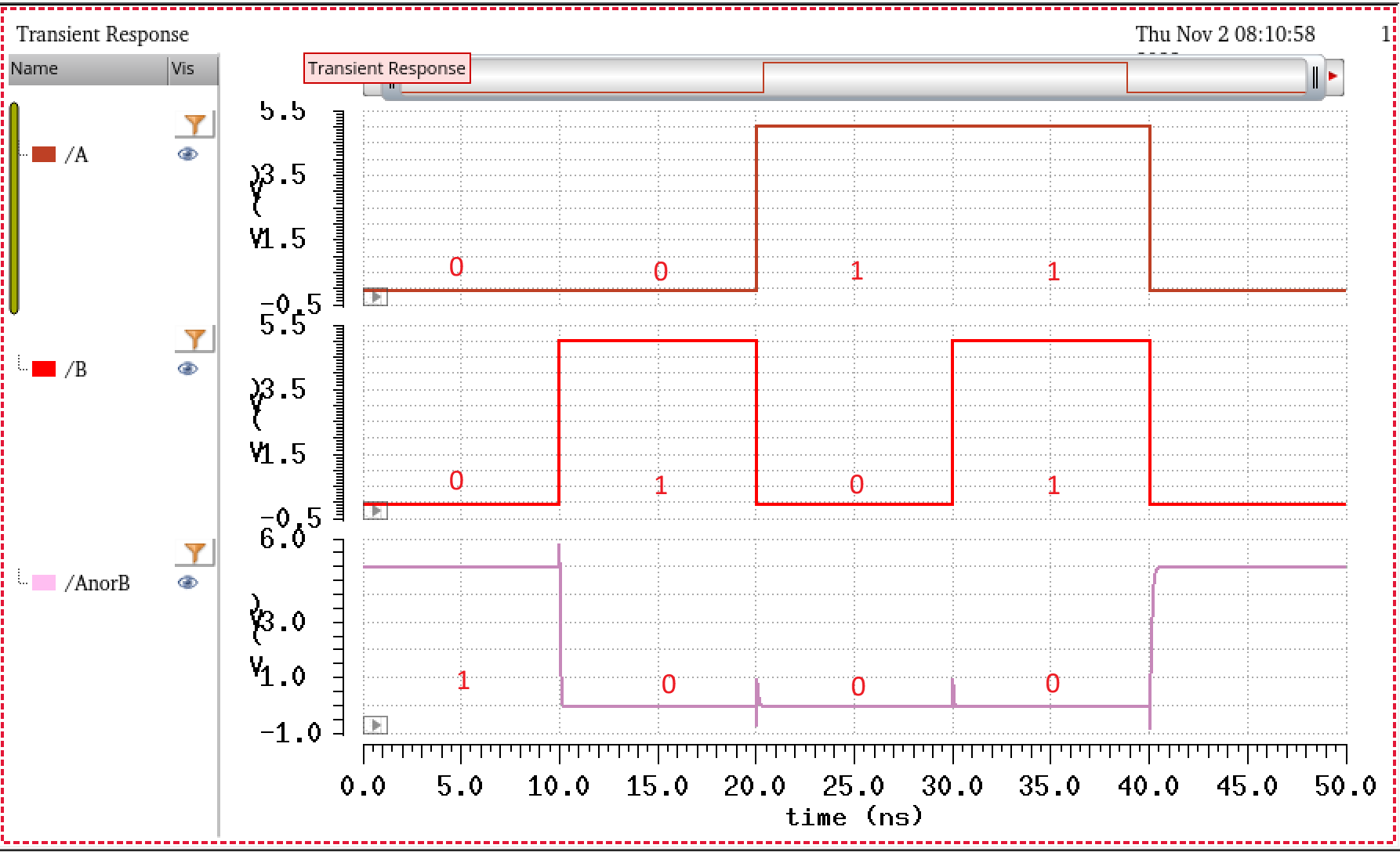
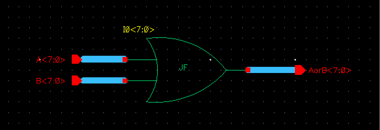
Now that we know that the NOR gate is working properly, we can proceed to making the 8-bit input/outputs gate. We start be instantiating the NOR gate above, in an array as seen below, and attaching an bus wires to each input and output. Noting that we must have 8 wires in the bus for A and B, since we are creating 8 NOR gates.
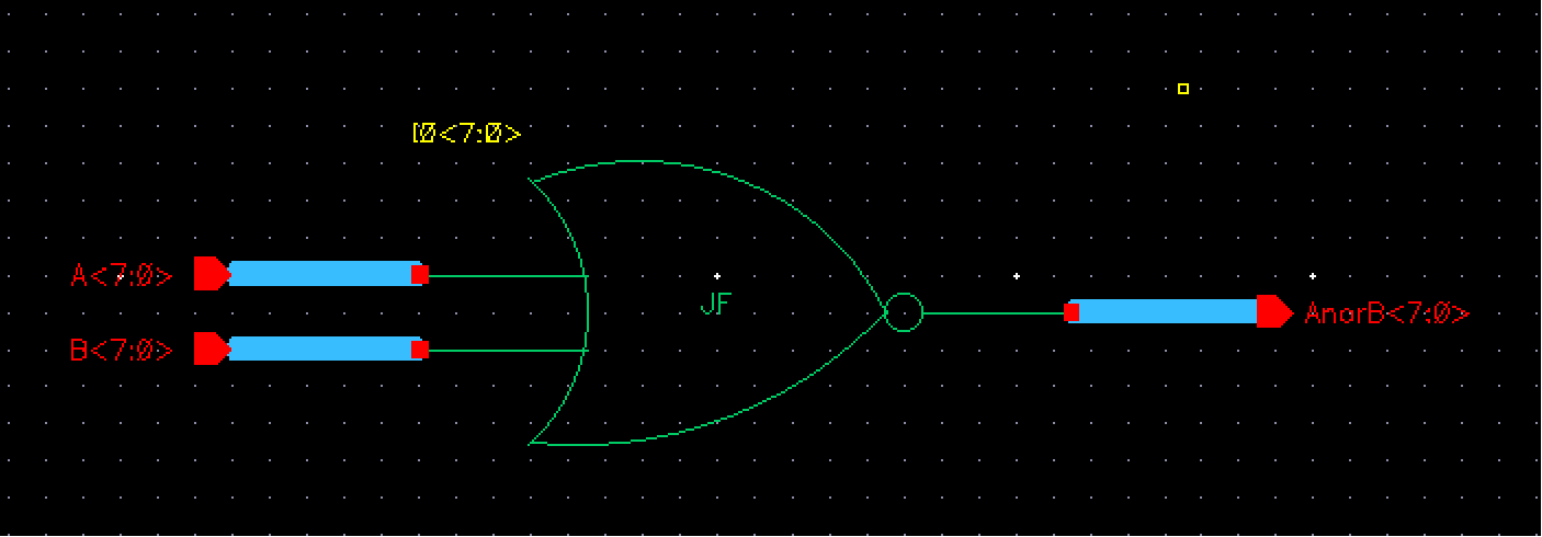
The symbol for this 8-bit input/output NOR gate is then:
8-bit input/output OR Gate
For the OR gate, like previously done, we will add an inverter infront of the NOR gate to create our desired output.
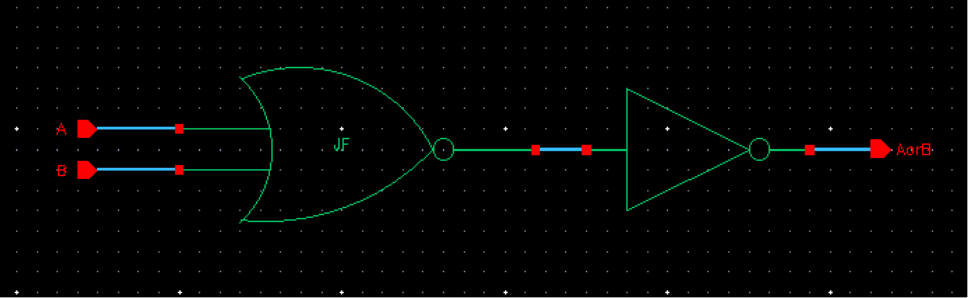
The symbol is then:
For the 8-bit input/output schematic can now be drawn as seen below:
The symbol is then:
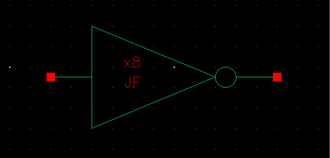
8-bit input/output Inverter
This inverter is the same as the one made in Tutorial 5, but with 8-bit input/outputs this time. The changes result in the following:
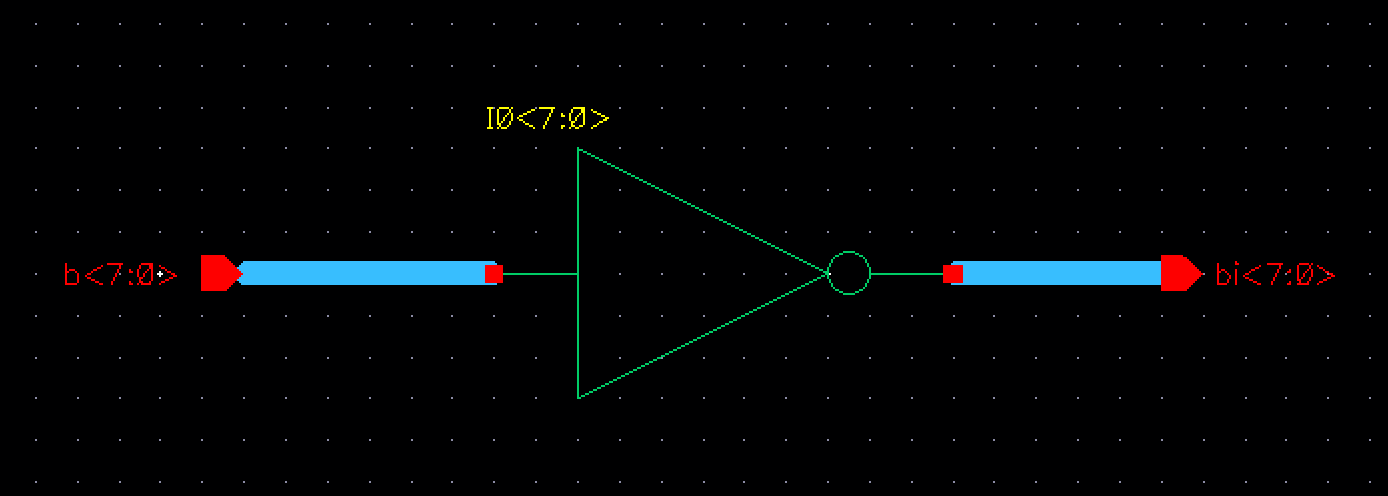
The symbol for this 8-bit inverter:
Simulation for all Gates in one
Finally, we are now ready to throw all the 8-bit input/output gates made above (i.e NAND, AND, NOR, OR, and inverter) into a single schematic cell view for simulation. This will save us time since all we need to look at is one wire from each gate. All other wires are an exact replica. For this simulation, I chose to probe wire <0> of each gate. Below is the schematic:
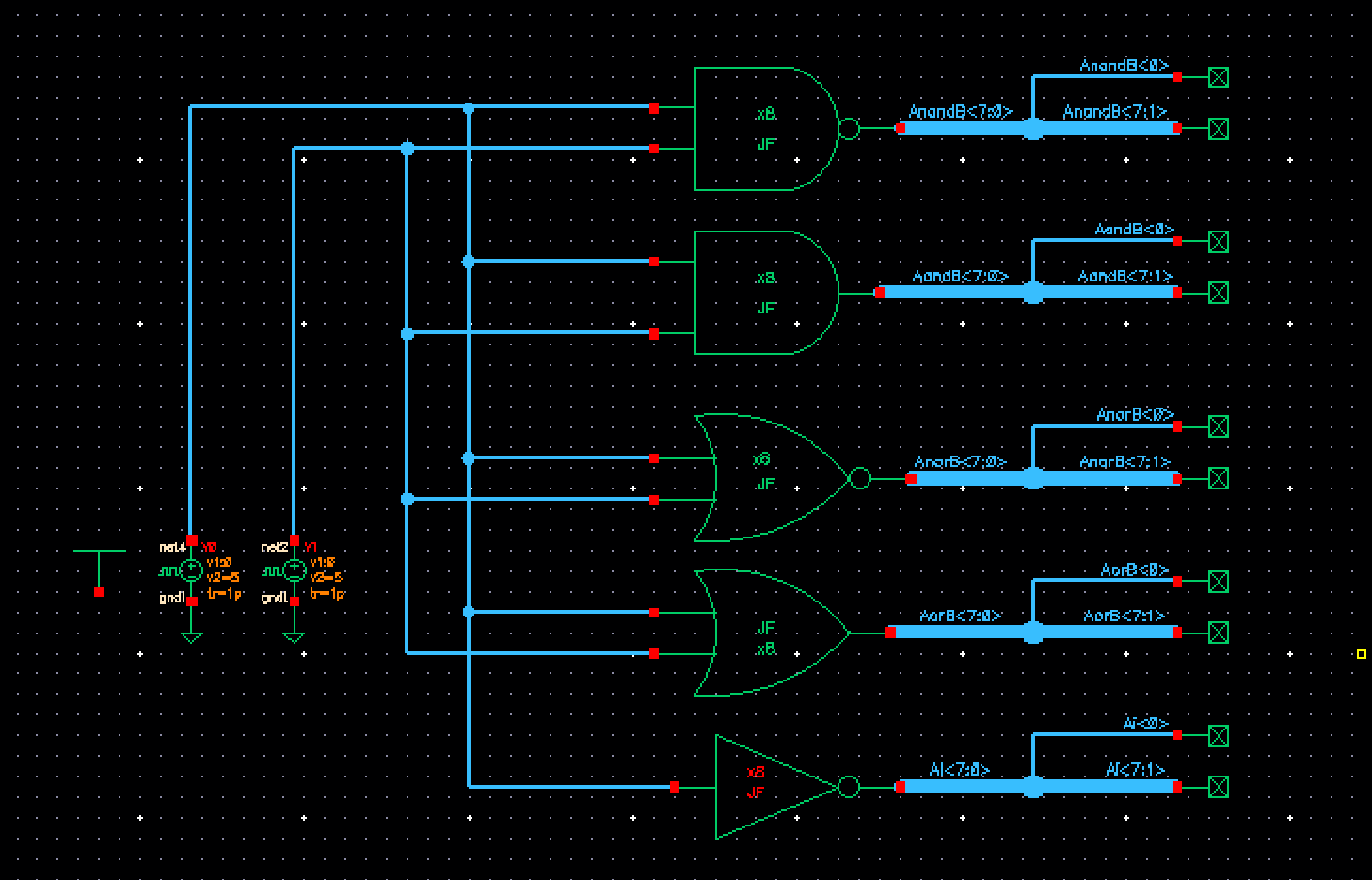
Just to refernce our outputs in the simulation, Ill provide the truth table for this schematic below followed by the simulation results. Note that the inverter only take A for the input.
Truth Table for Schematic
| A | B | AnandB<0> | AandB<0> | AnorB<0> | AorB<0> | Ai<0> |
| 0 | 0 | 1 | 0 | 1 | 0 | 1 |
| 0 | 1 | 1 | 0 | 0 | 1 | 1 |
| 1 | 0 | 1 | 0 | 0 | 1 | 0 |
| 1 | 1 | 0 | 1 | 0 | 1 | 0 |
2:1 Mux
Below you will find the schematic for the 2:1 MUX
The corresponding symbol is then:
We can then setup the schematic to simulate the mux, as see below. Note that the inverter is applied to get our input Si.
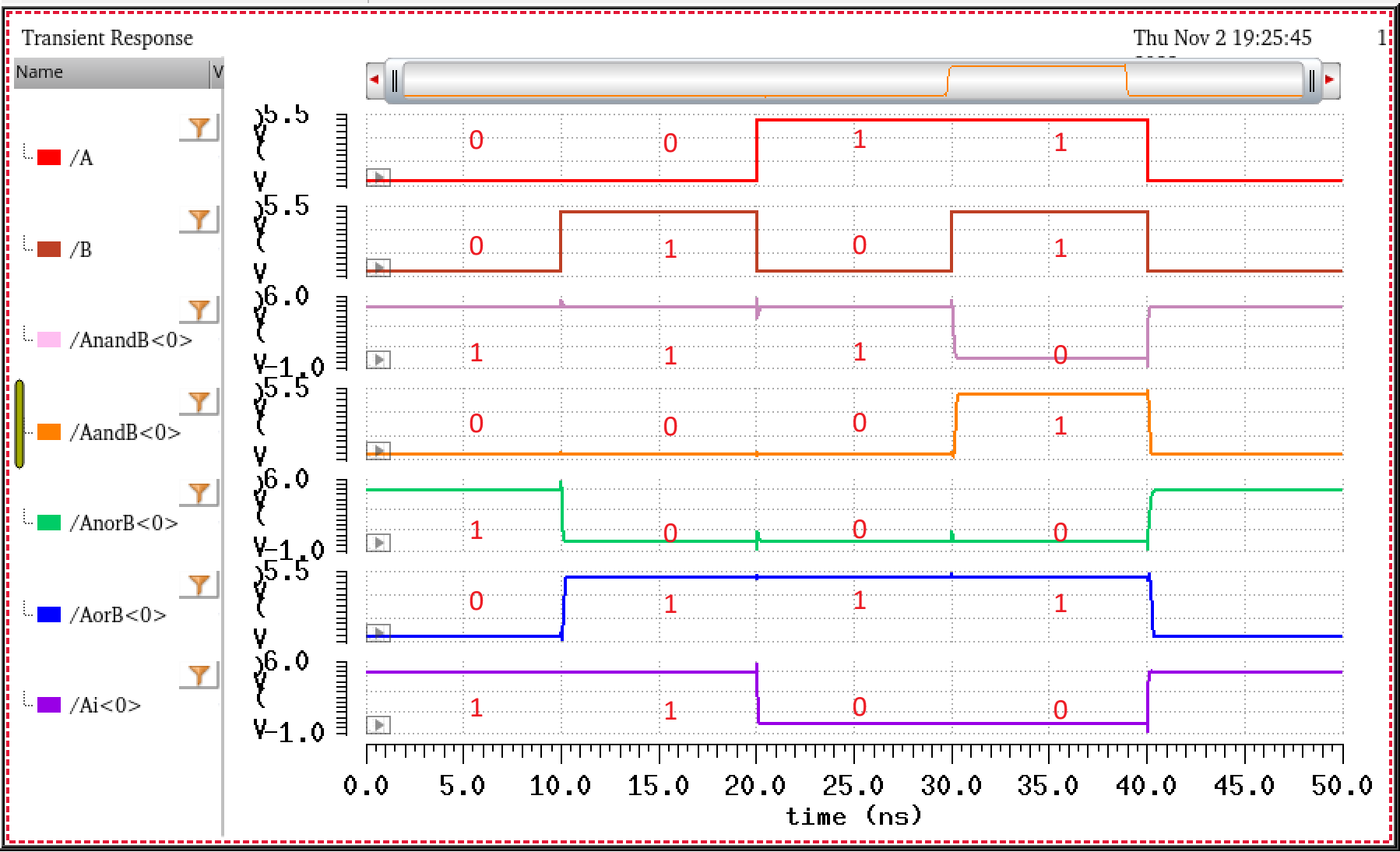
Simulation then yields:
In this simulation, you can see that whenever S is low, the MUX output, Z, follows B. When S is high, the ouput then follows A. In other words, from a multiplexers point of view, we can say that our select line is S, and we have data A sitting in position 1 of the multiplexer, and B in position 0. Meaning that when S is high, output will get A, and whenver S is low, output will get B.
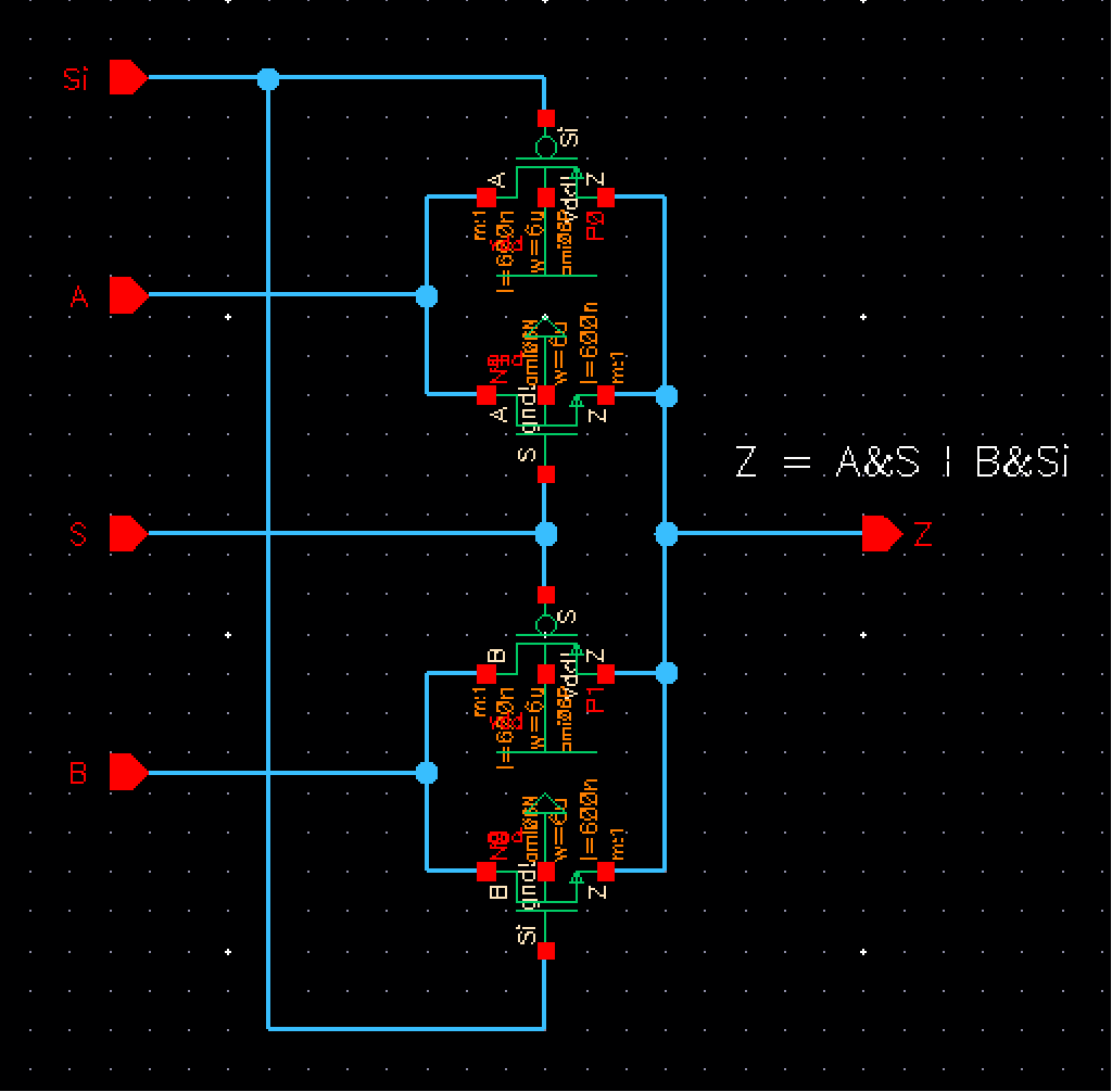
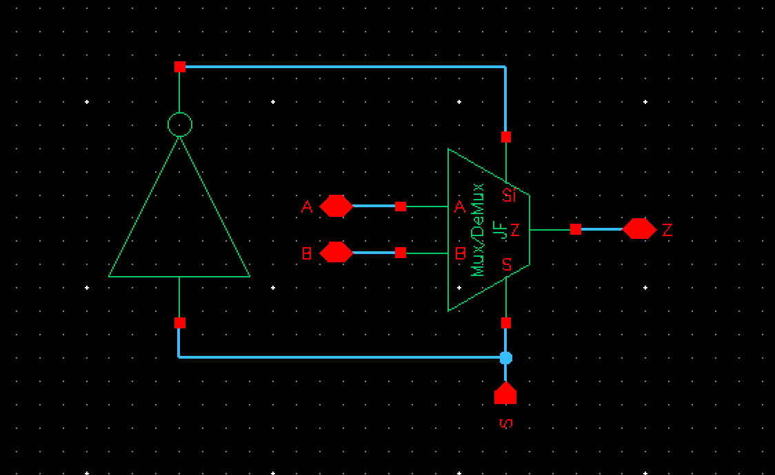
2:1 Mux/DeMux
For the creation of the Mux/DeMux, we can simply use the 2:1 Mux created above, but this time our A, B and Z pins will have a input/output property. This way we're allowed to have Z as an input, as opposed to the above schematics where we only defined it as an output. Similary for A and B, we will assign them as input/output pins.
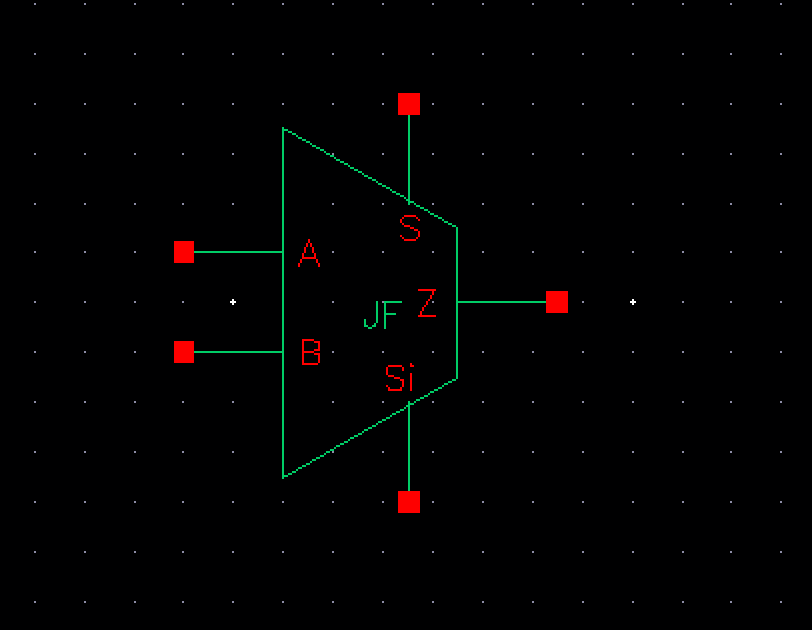
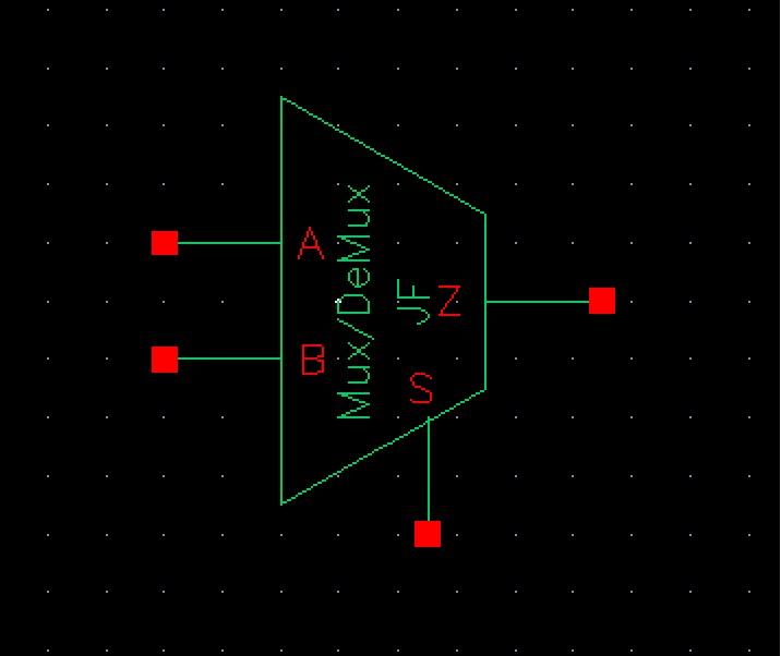
To differ from the original 2:1 Mux, we will change the symbol to have its name as seen below:
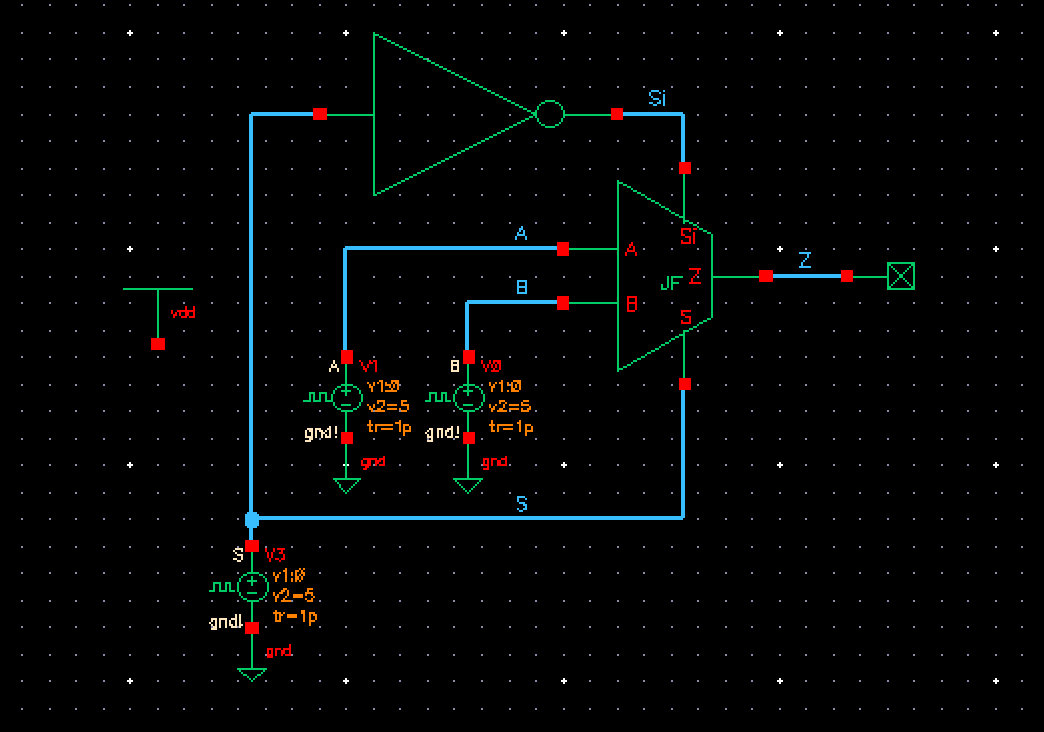
Using the same simulation schematic as the 2:1 Mux, but with different parameters is seen below. In this schematic you will notice that we will be using Z as the input, S is still our select line, while A and B will be our outputs.
The simulation to this schematic yields the following:
The results yield what we would expect from a DeMultiplexer. In this new setup, we can see that while S is low, the output that gets Z, is B. When S goes high, A then follows Z. In other words, similar to the 2:1 simulated before, our select line S selects which output should get Z. In comparison from the Mux, the DeMultiplxer is the inverse of it so to speak. Simulations above matches what we would expect.
As this DeMux handles both directions, that is, A, B and Z being inputs/outputs, there is no need to simulate the other direction, as it will look exactly the same as the Mux simulated before this section.
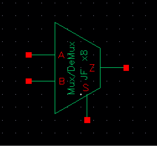
8-bit Wide Word 2:1 DeMux/Mux
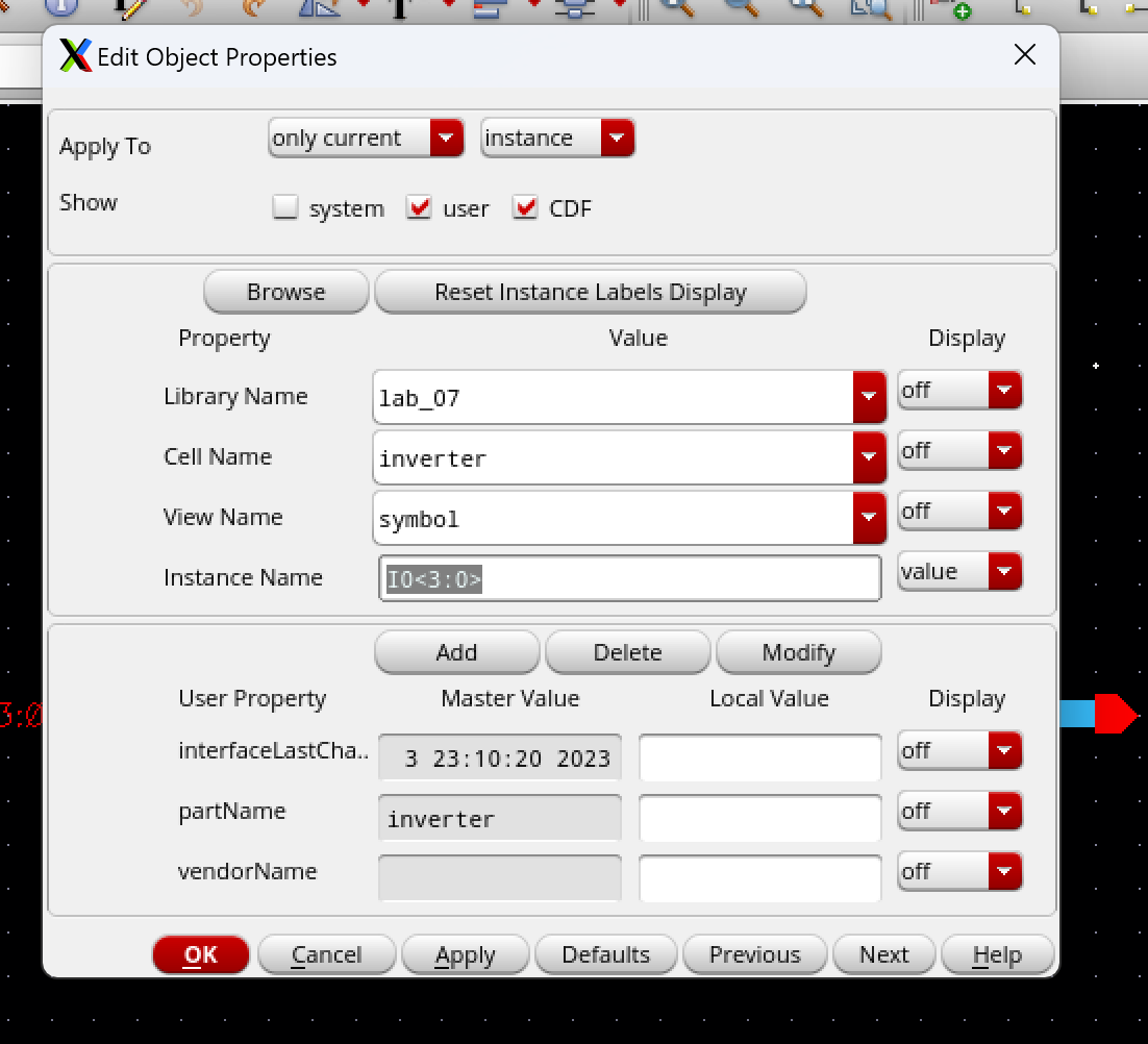
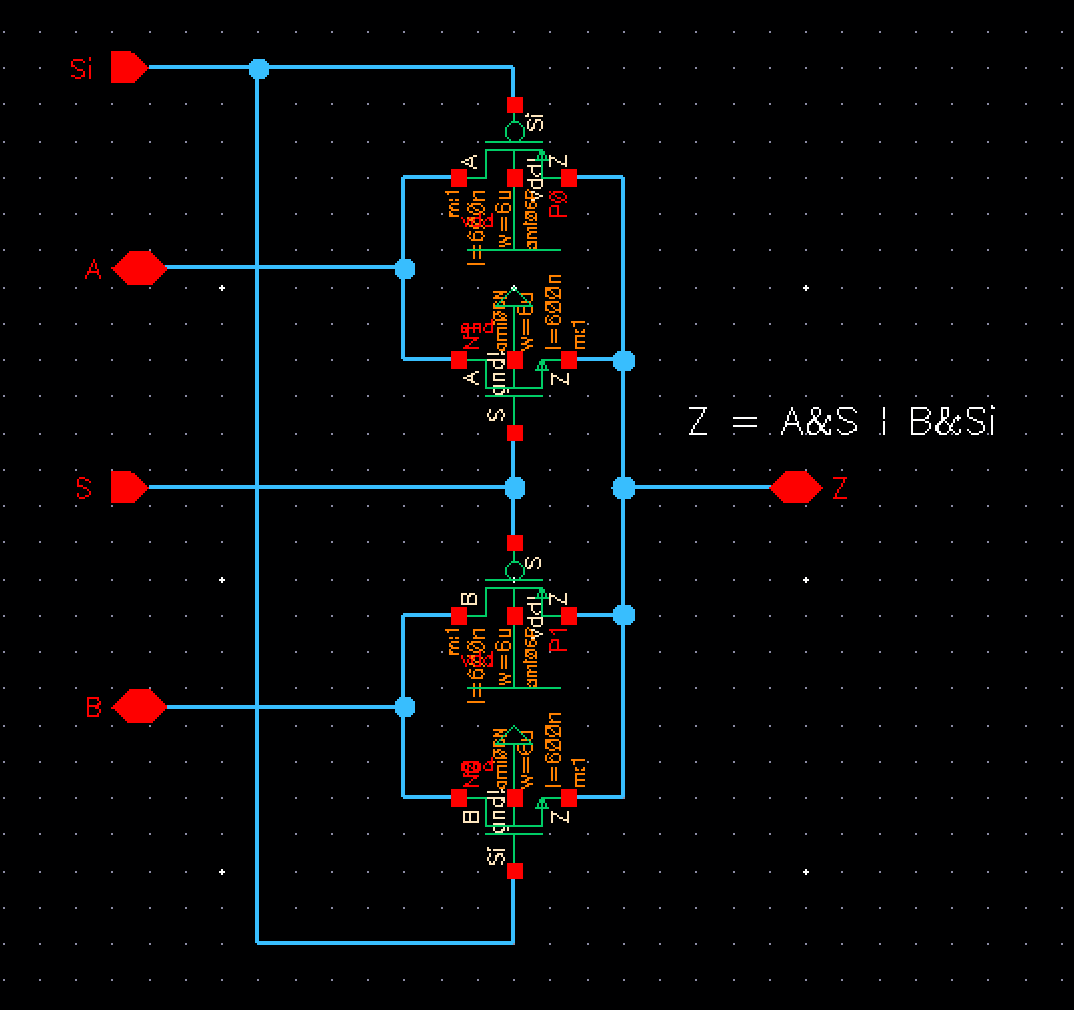
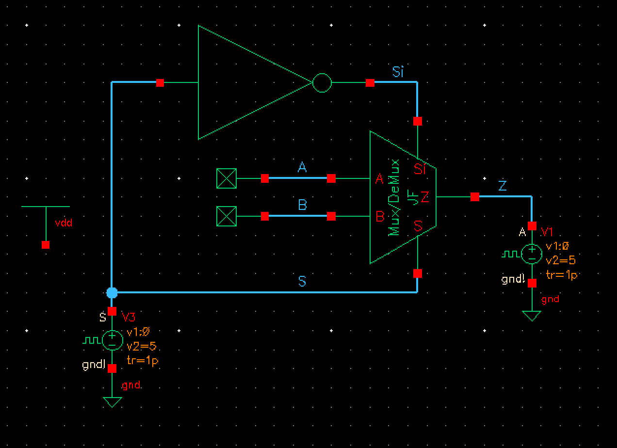
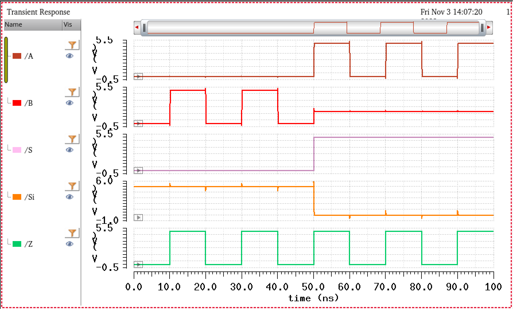
For this 8-bit word design, we will implement the DeMux created above, but this time we will make a new cell view, that only takes in one select line S for the input. Si will be generated inside of the scheamtic as seen below.
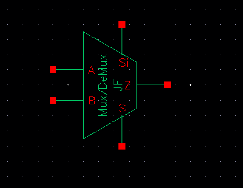
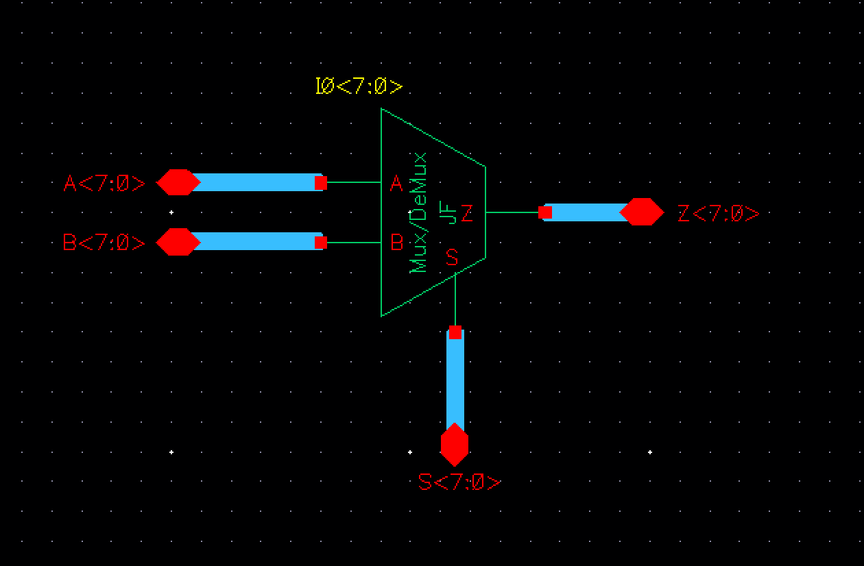
With this schematic setup, we only need one input for S. We can then redraaw this new symbol as below.
Finally we can setup the 8-bit word DeMux as below. Process is the same as previous gates.
The symbol for this is:
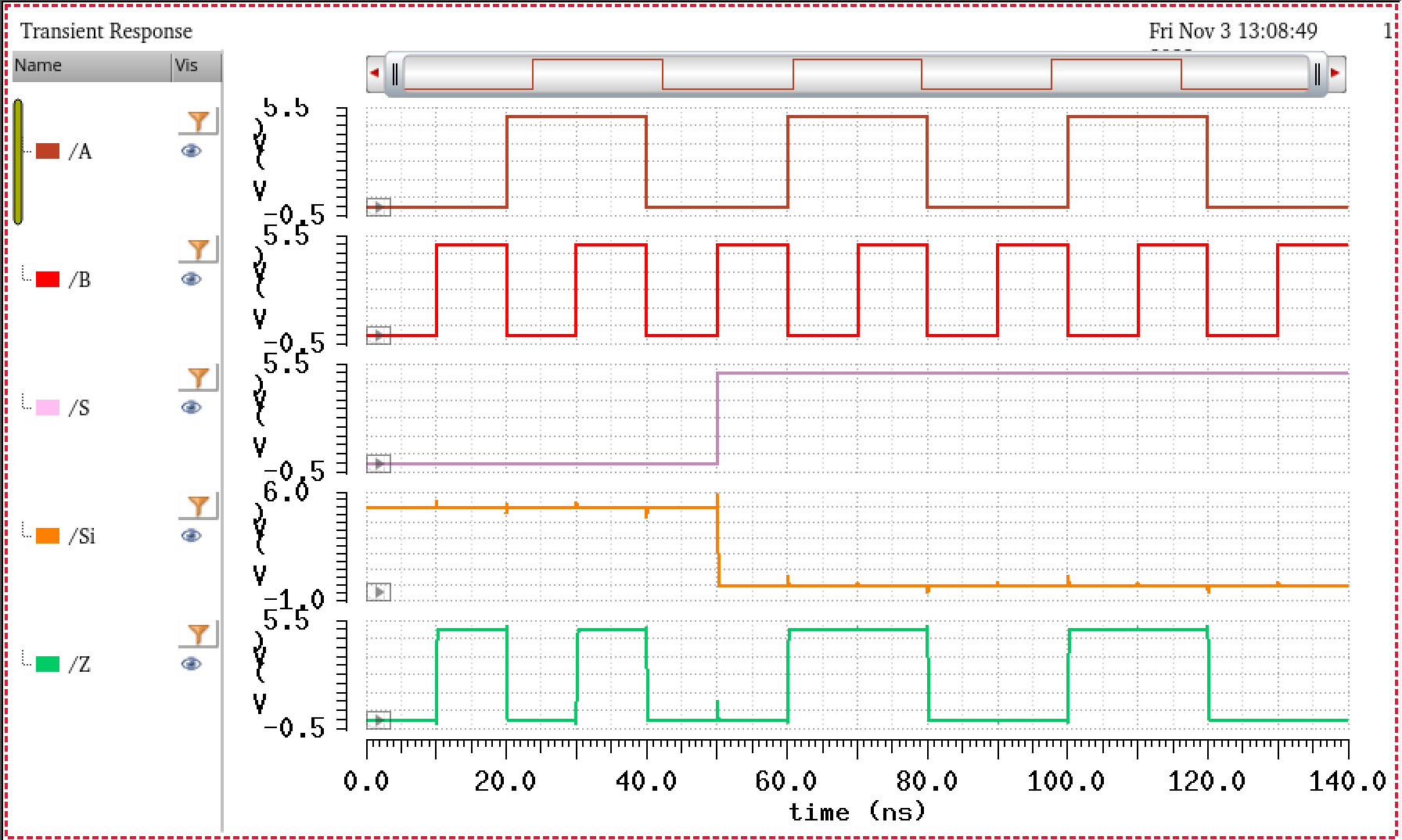
Setting up the simulation schematic we get the following:
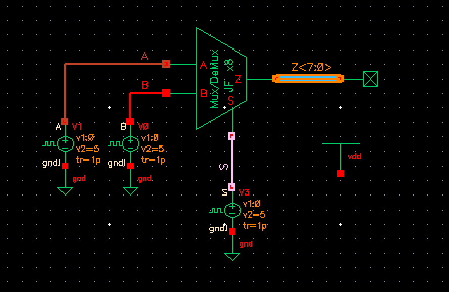
Results are the following:
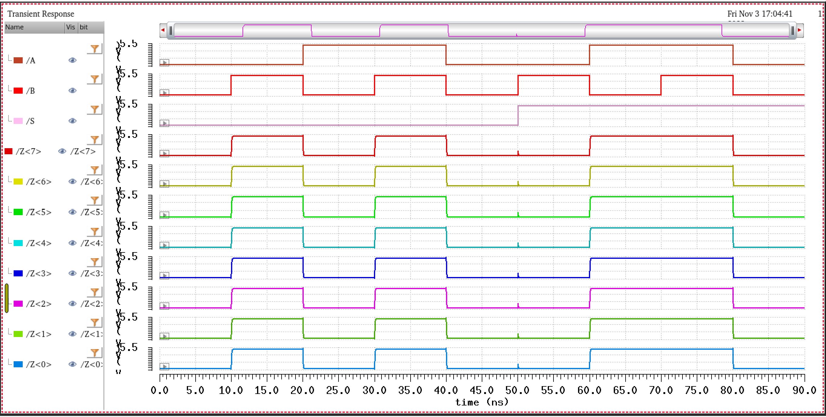
From the results above,we can confirm that each output is exactly the same, and as from before, when S goes high, the output follows A, and when S is low, output follows B.
Full Adder
Now for the last experiment we will implement the full adder schematic
shown below:
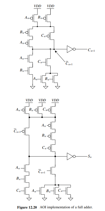
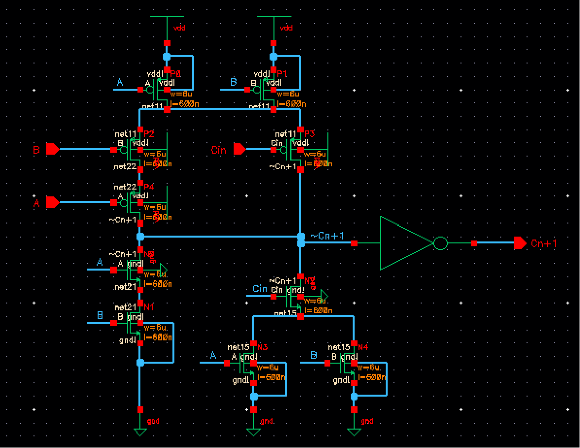
Schematic Overall View:
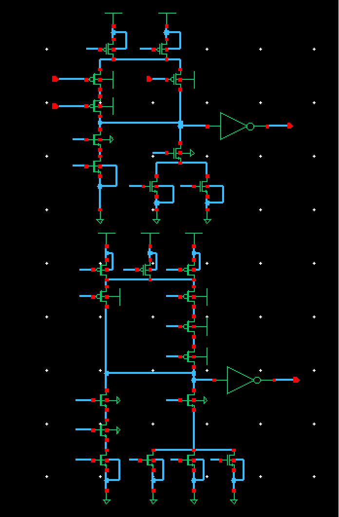
Zooming into each section, heres the upper half view:
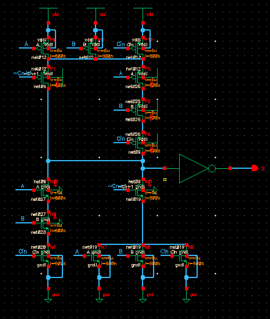
Lower half:
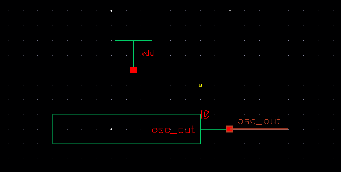
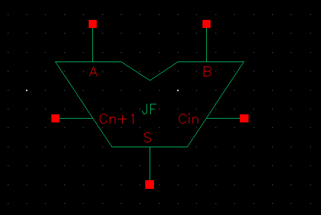
The corresponding symbol is the same as last lab as shown below:
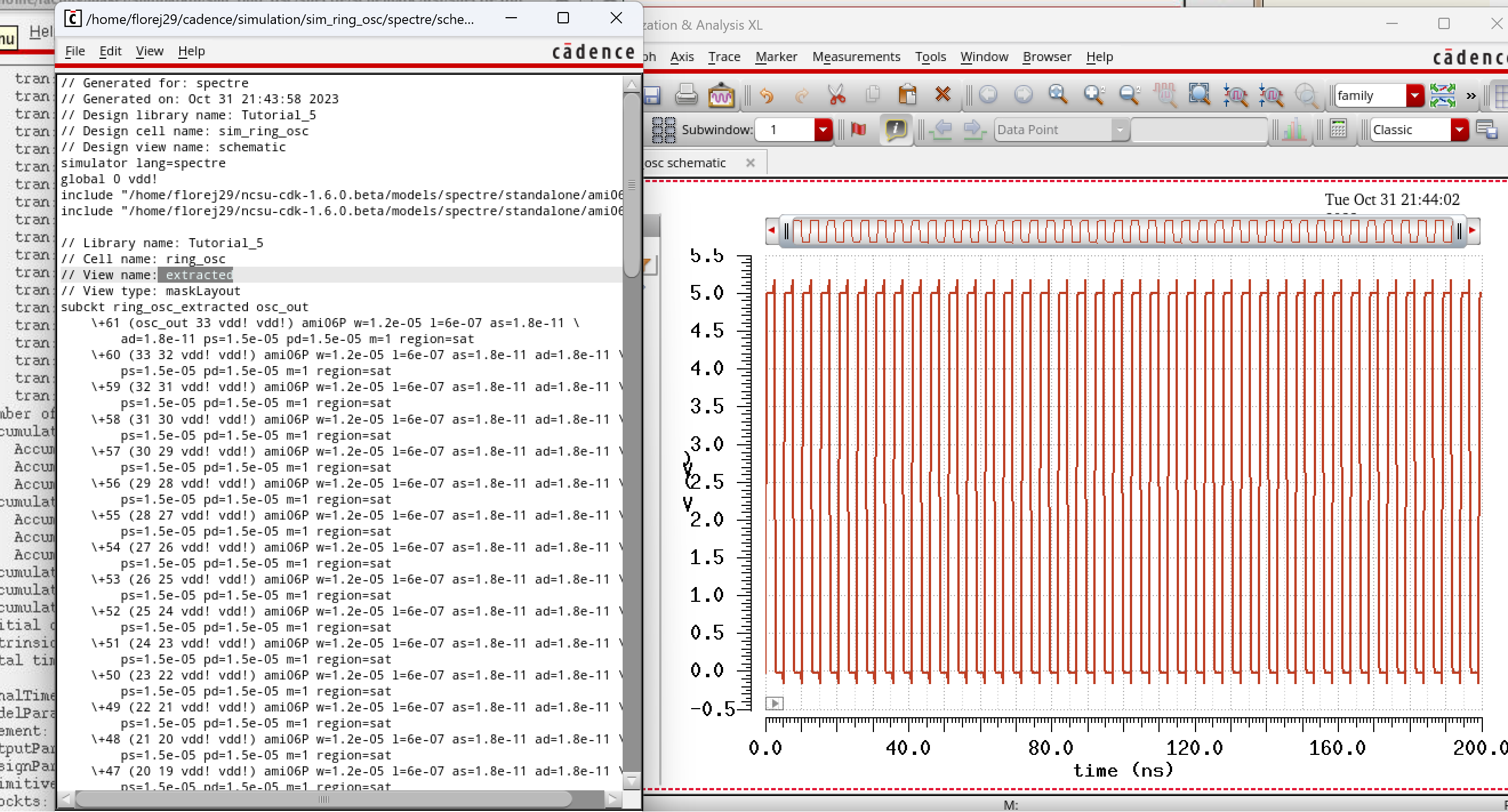
Before proceeding making the 8-bit full adder, let us make sure the design works properly by simulating just this single full adder.
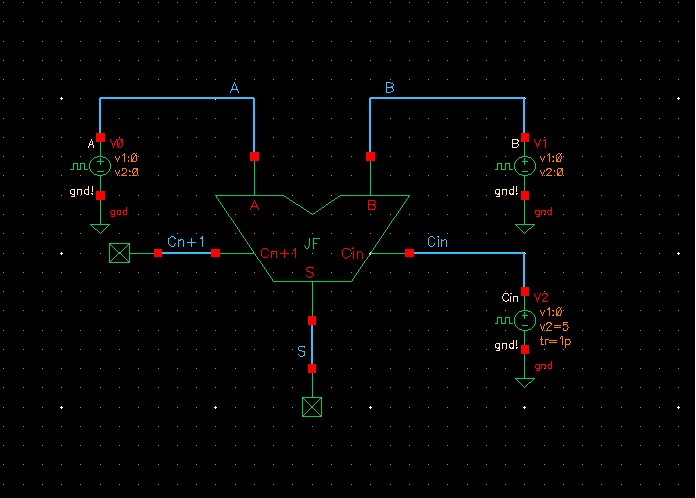
Simulation yields:
| A | B | Cin | S | Cn+1 |
| 0 | 0 | 0 | 0 | 0 |
| 0 | 0 | 1 | 1 | 0 |
| 0 | 1 | 0 | 1 | 0 |
| 0 | 1 | 1 | 0 | 1 |
| 1 | 0 | 0 | 1 | 0 |
| 1 | 0 | 1 | 0 | 1 |
| 1 | 1 | 0 | 0 | 1 |
| 1 | 1 | 1 | 1 | 1 |
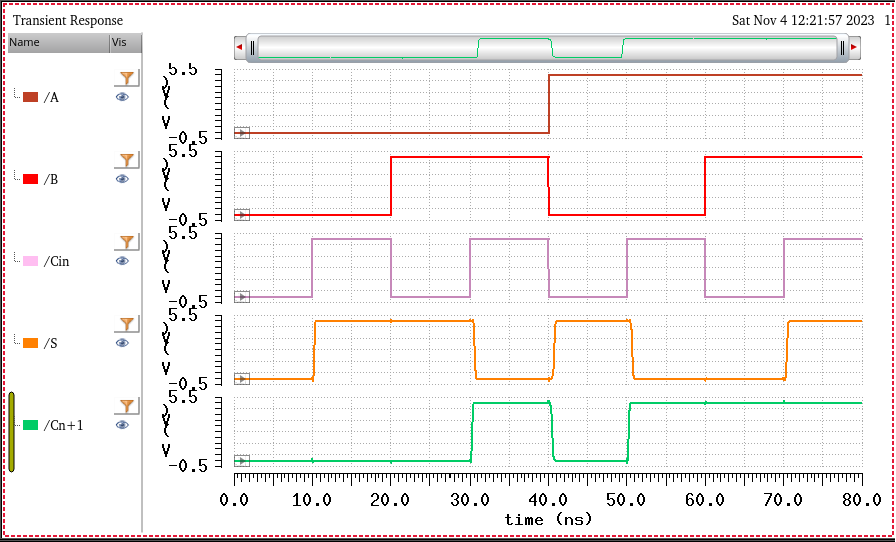
The simulation results in the correect outputs as our truth table. Now we can create the 8-bit word wide full adder.
8-bit Full Adder
The schematic is seen below:
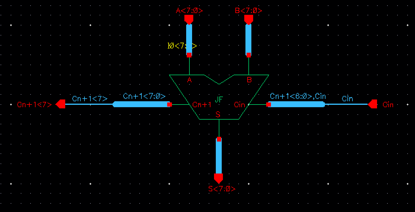
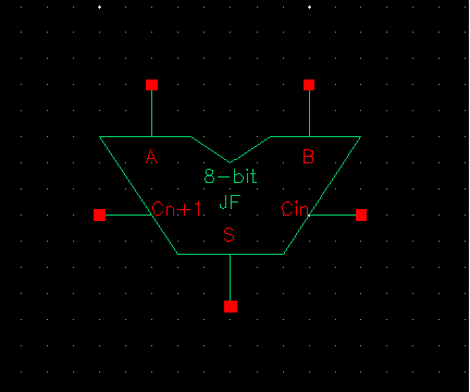
Symbol for the 8-bit Full Adder is then:
For the simulation we will add 2 8-bit binary numbers. Below you will find the input values as well as the simulation following it to confirm the full adder works properly.
*No carry in bit*
A[7:0] = 0100 _0111 = 71 (in decimal)
B[7:0] = 0001_1111 = 31 (in decimal)
S[7:0] = A + B = 0110_0110 = 102 (in decimal)
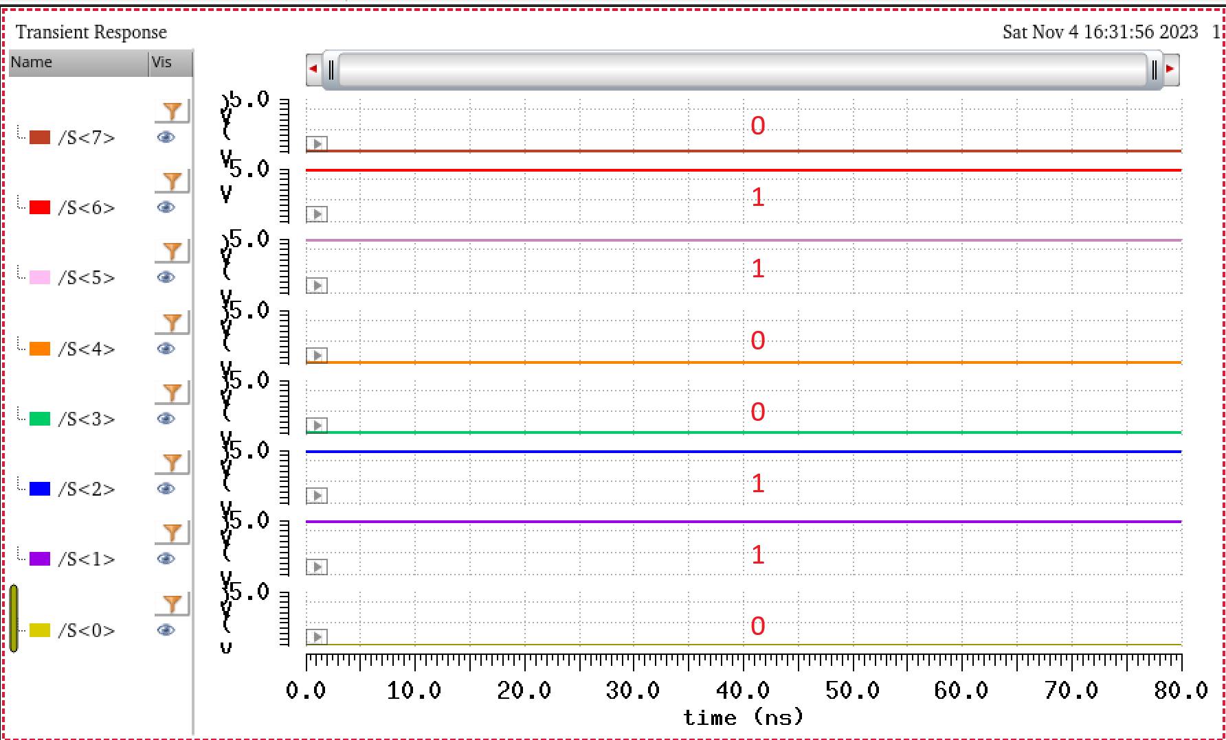
The results yield the S value expected as seen above. Now lets add a carry in bit to make sure that works as well. The bottom bit S<0> should change to 1.
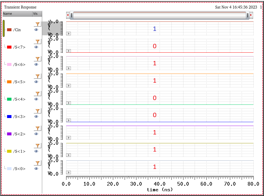
The results are exactly what we expected, therfore we're good to proceed onto the next step :).
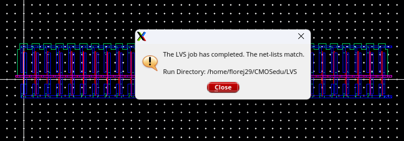
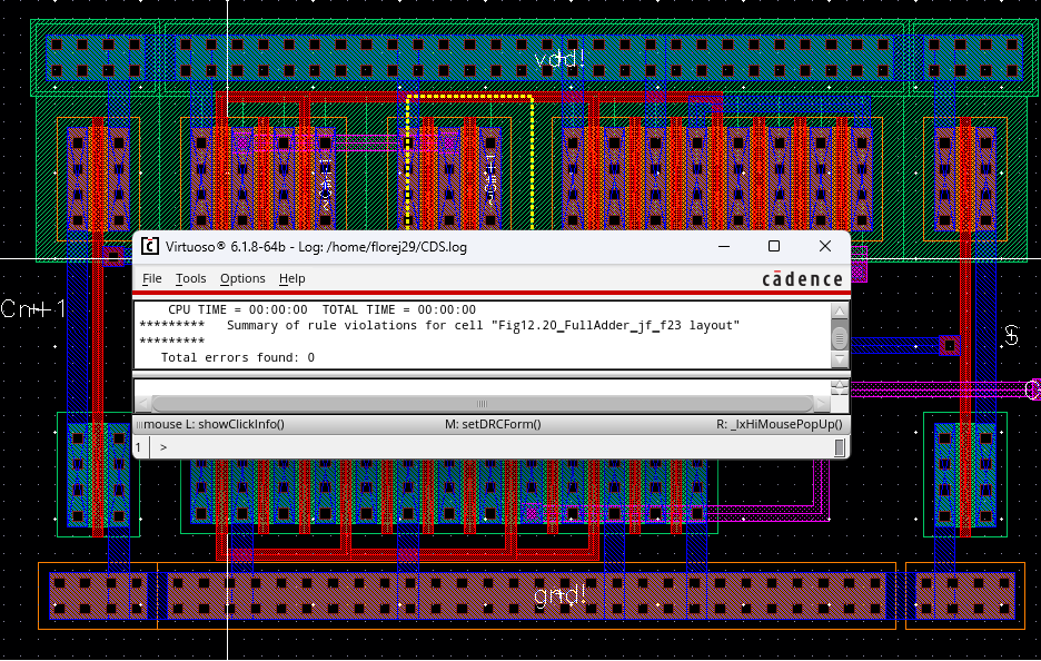
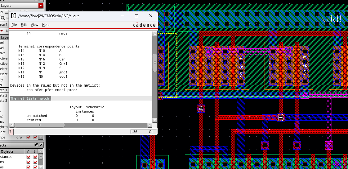
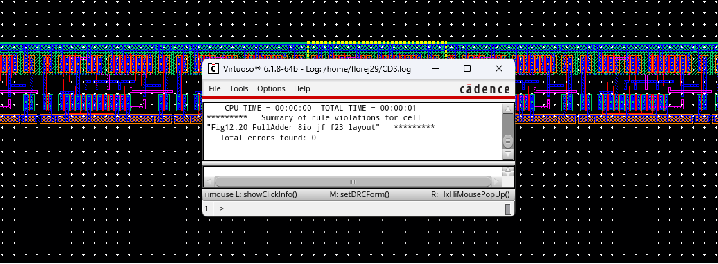
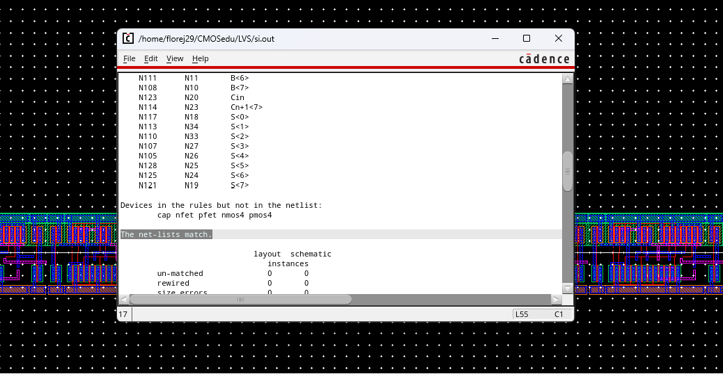
Before continuing with the 8-bit layout, we must successfully complete the layout for the single full adder. Below you can see the layout of a single full adder, as well as the clean DRC and LVS.
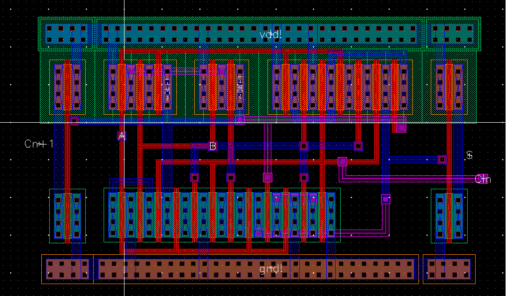
Extracted View:
DRC and LVS Pass:
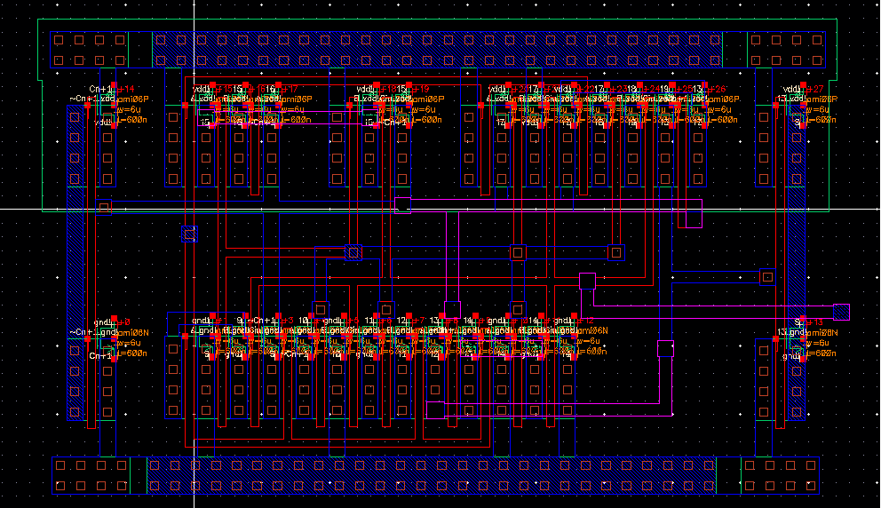
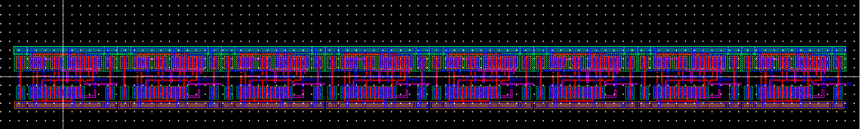
Now that we have a clean full adder layout, we can proceed with the 8-bit full adder layout.
Overview of the entire layout:
Left Side Zoomed in:
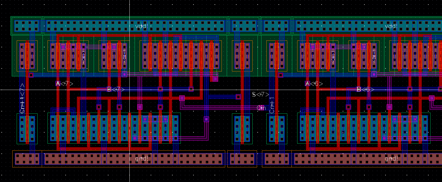
Right side:
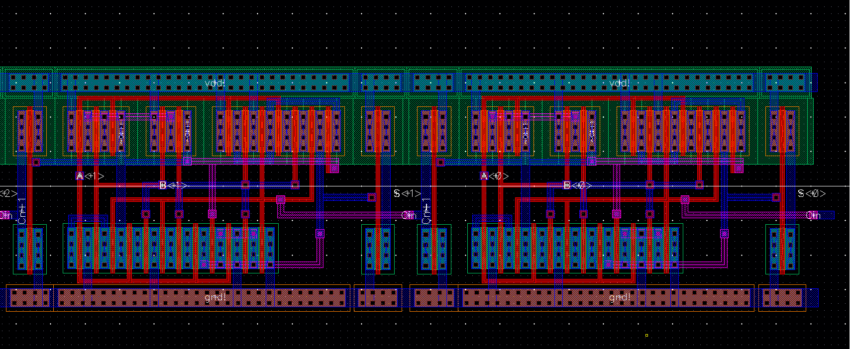
DRC and LVS Pass:
This concludes Lab 7. Below you can find my lab files for lab 7.
>> Lab 7 <<