Lab 6 - EE 421L
Authored
by Jesus Flores-Arellano
Email: florej29@unlv.nevada.edu
October 13, 2023
Lab
description
- During this lab we will design, layout and simulate a CMOS NAND gate, XOR gate, and a full-adder.
Prelab Tasks
- Backup up previous work
- Go over Tutorial 4 before starting lab 6.
- Read through lab 6 document and its enterity before starting to work on it.
Prelab
We
first copy Tutoria_3 library from last lab, and rename it Tutorial_4.
Right after we can also copy the "inverter" cell and rename is
"nand2". This will be our cell for the design of the nand gate with 2
inputs.
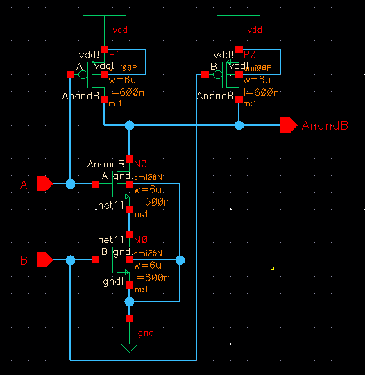
We can then edit the schematic of our new "nand2" cell and change it the nand gate schematic as seen below:
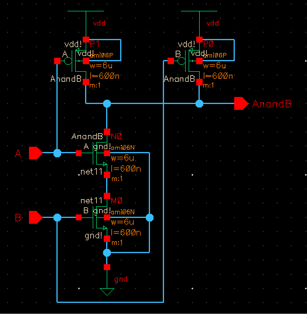
Note
that when we first check and save after doing this change, we will get
warning markers, since the symbol view of the old schematic is not
matching up with our new schematic. We can simply delete the old symbol
view, and check and save the new schematic again. This should fix the
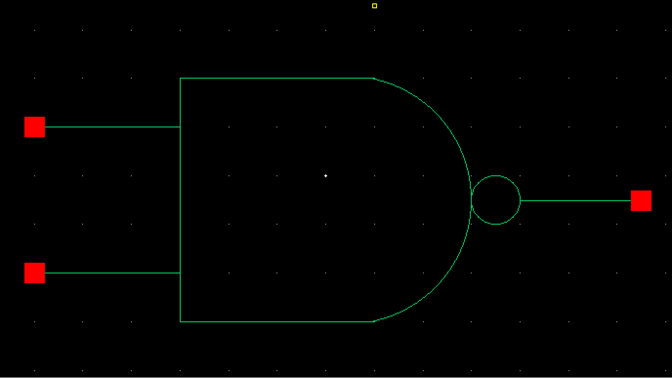
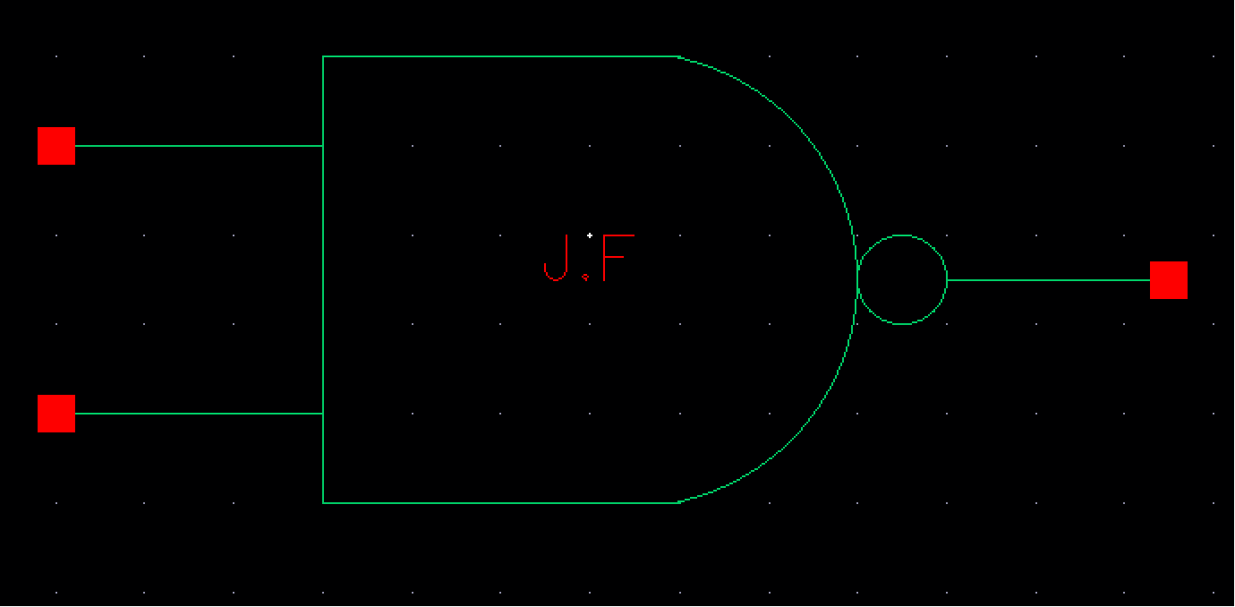
warnings, and now we can creaet our new symbol view for NAND gate as
seen below.
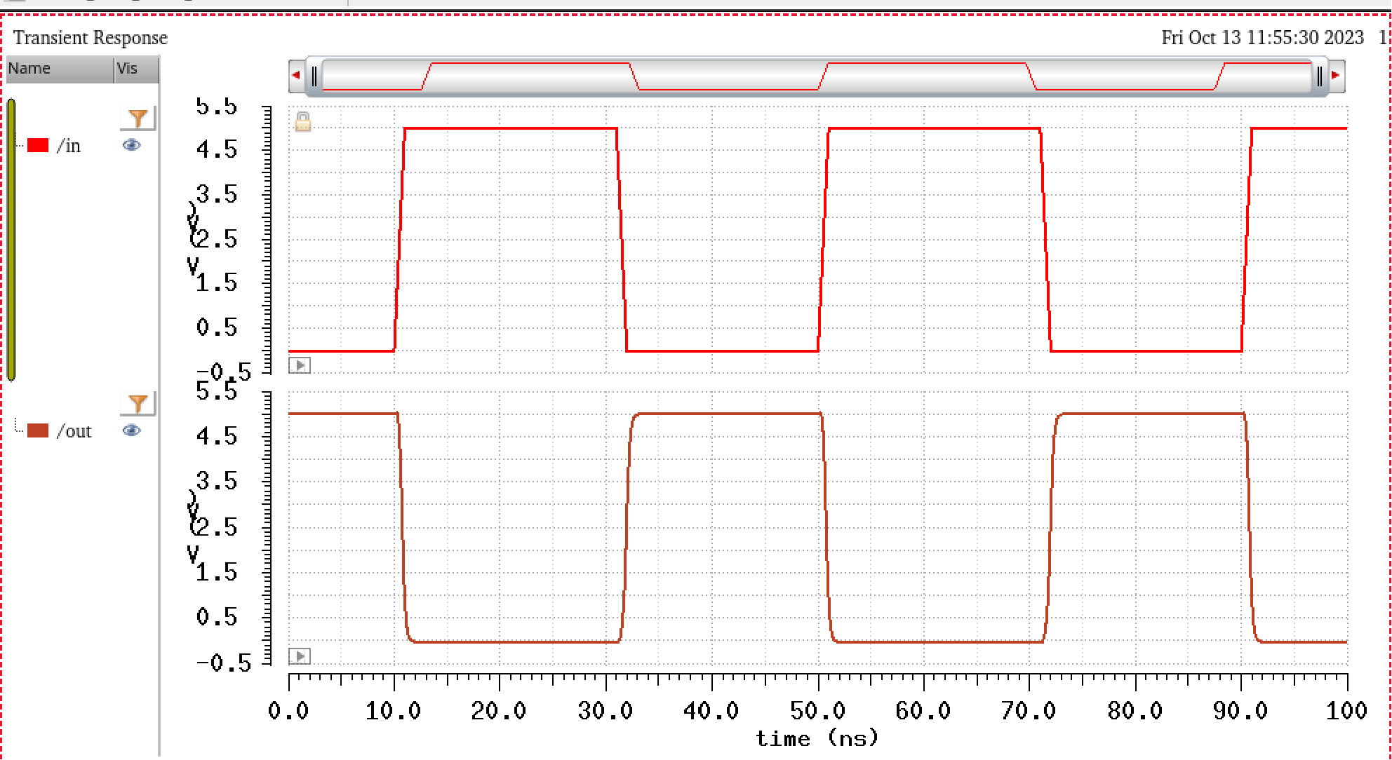
We can then move onto simualating the operation of this NAND gate.
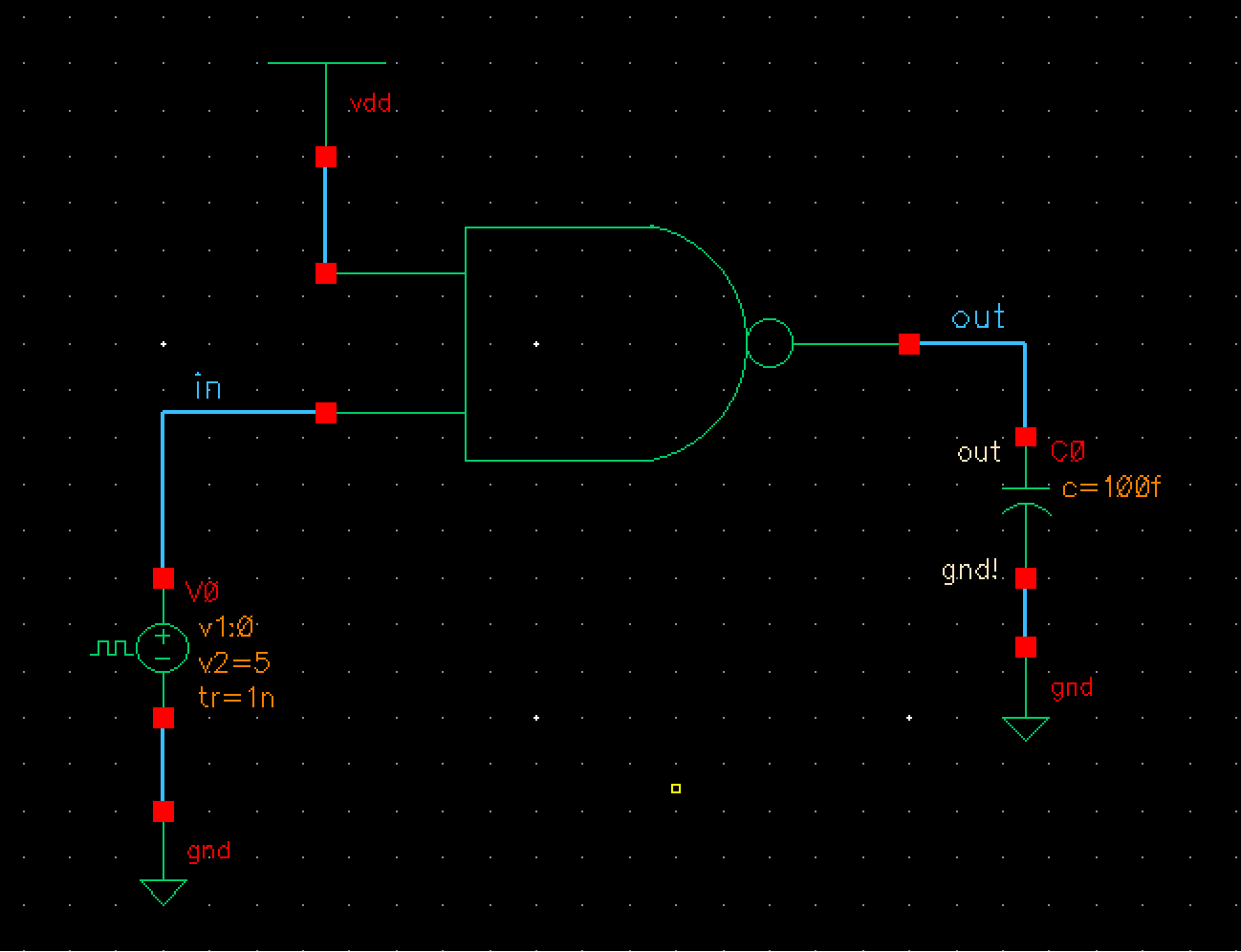
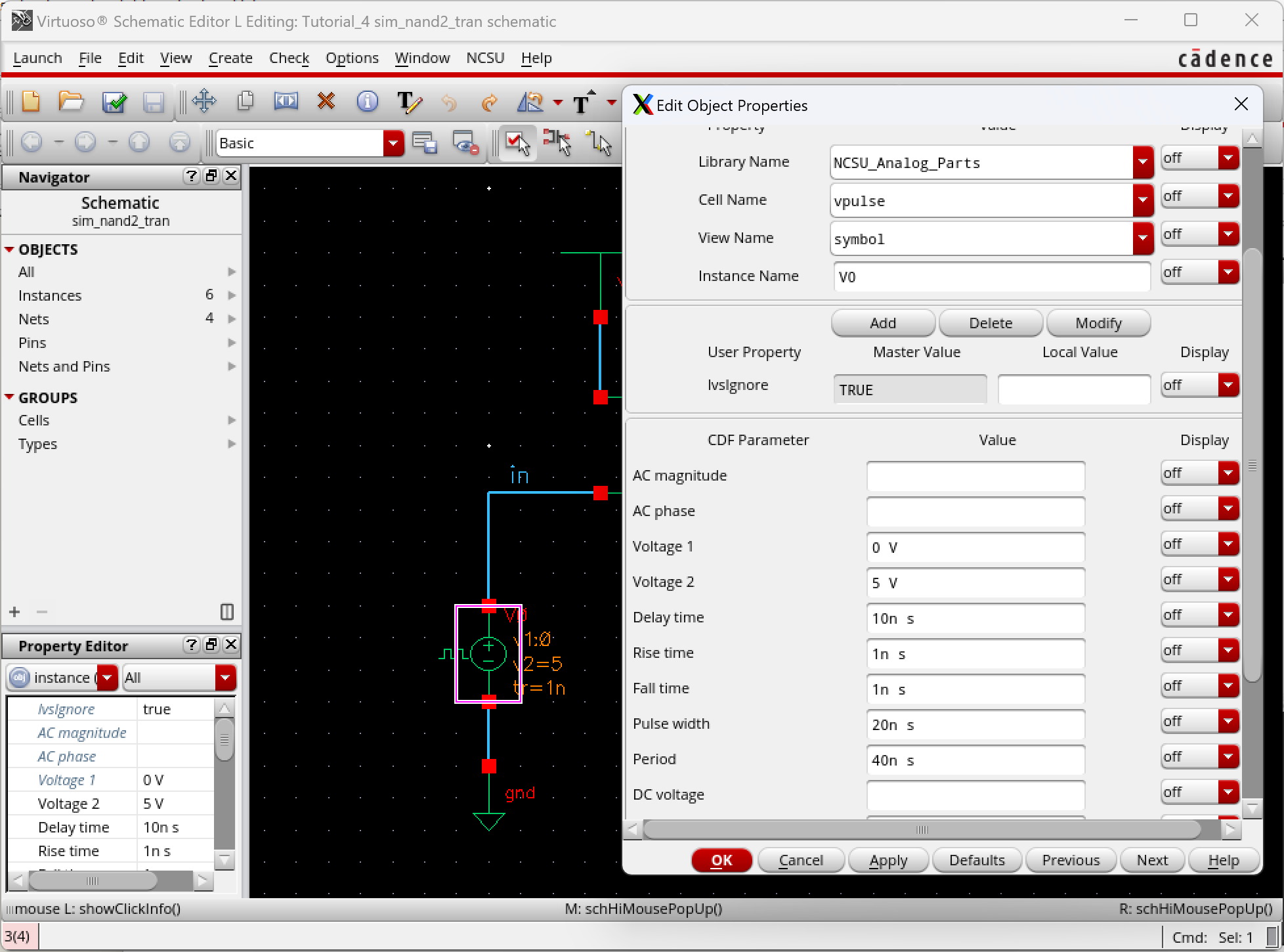
Setting up the schematic, and showing the voltage pulse settings for future reference,:
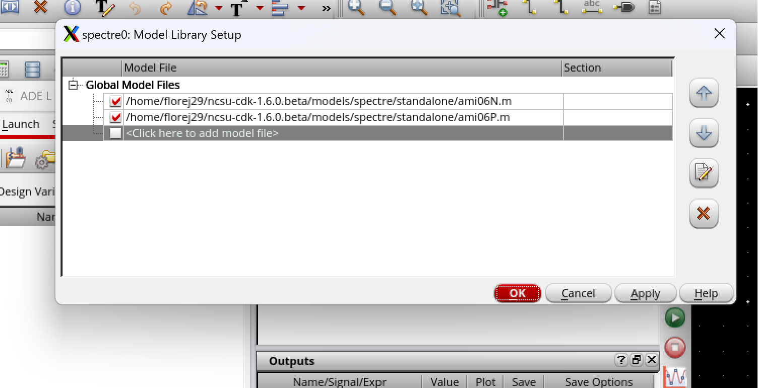
We then launch ADE L, and add the model librarires for the pmos and nmos as seen below.
We
then give vdd! a value either through the Stimuli or add a voltage
source phsyically connected to vdd! as seen in tutorial 3. In my case I
will use Stimuli. We navigate to Setup -> Stimuli, and we set
stimuli type to Global Source.
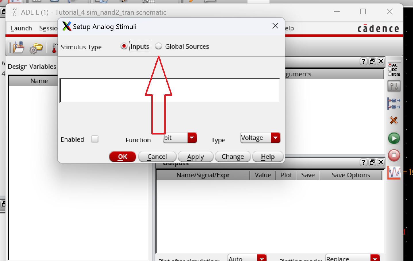
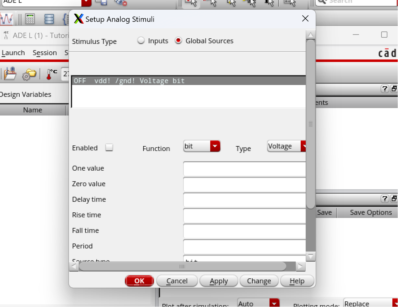
We
must change the function from "bit" to "dc" so that we can input the 5V
settings we wont for vdd! Note that the settings currently have enabled
turned off as seen below.
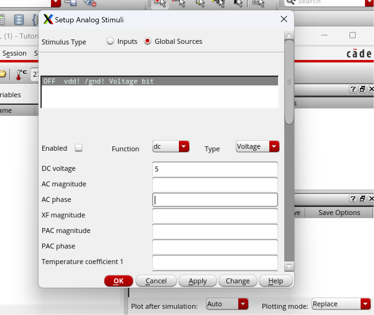
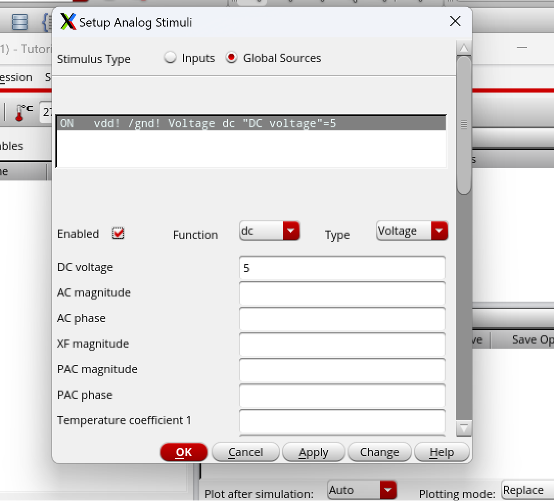
We must check the enable and hit Apply to see the settings change to "ON", meaning vdd! has a value now.
Now
we can just proceed to slecting the transient analysis with a stop time
of 100ns and the outputs being plotted will be "in" and "out".
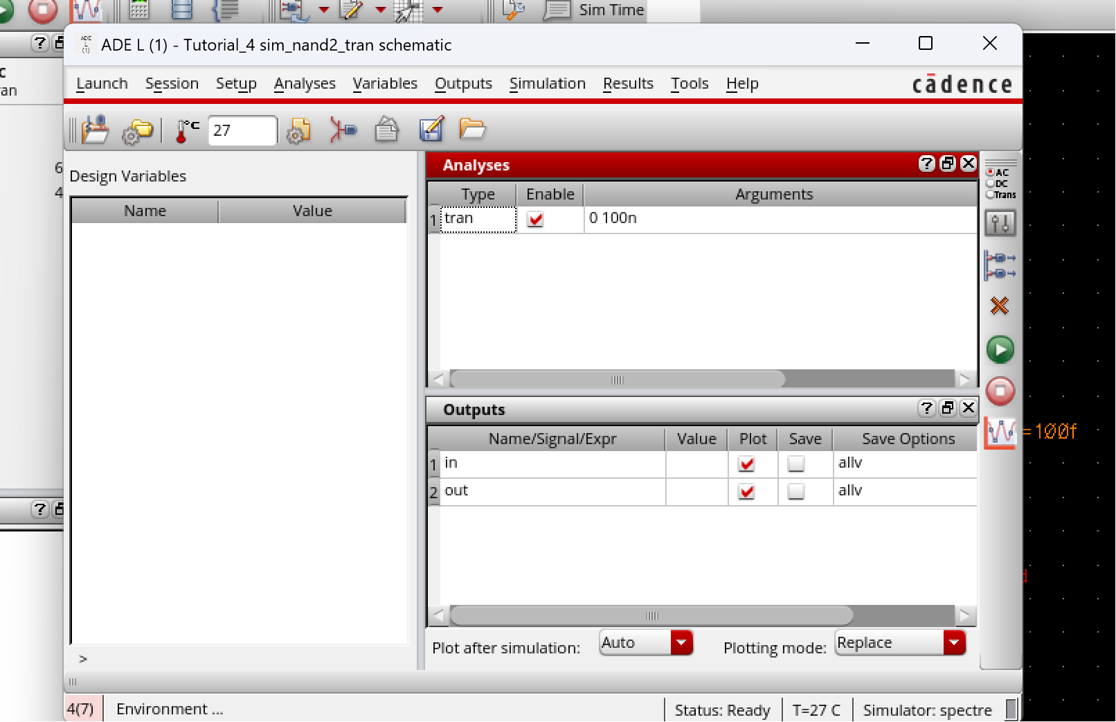
We then get the following:
Next
we proceed to doing the layout for this schematic. We can open the
layout of our new nand2 cell, and delete all the pins and metals that
were existing from the preivous inverter cell. We then duplicate the
PMOS and overflap it to look like the following. Note that the left
side of the duplicated PMOS is perfeetly overlapping the right
side of the original PMOS, meaning they will be sharing the drain.
Then,
we duplicate the NMOS and overlap it like we did with the PMOS above.
In addition, we can edit the ntap and ptap to 5 columns instead of 2,
and we move them as shown below:
Next,
we extend each poly and move the m1_poly to whats seen in the image
below. We will also add vdd!, gnd!, and B pins during this step, making
sure the B pin is created as an input pin.
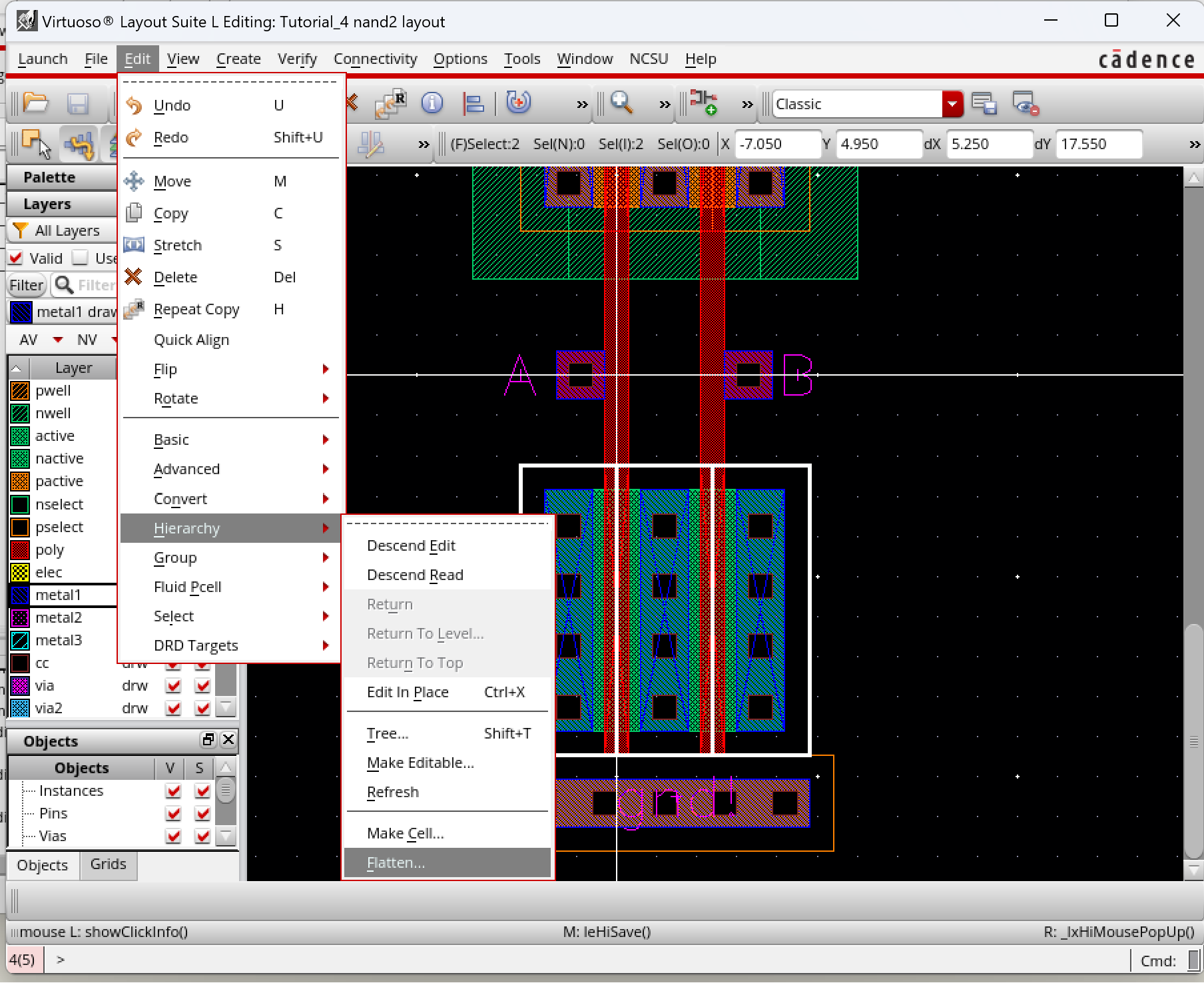
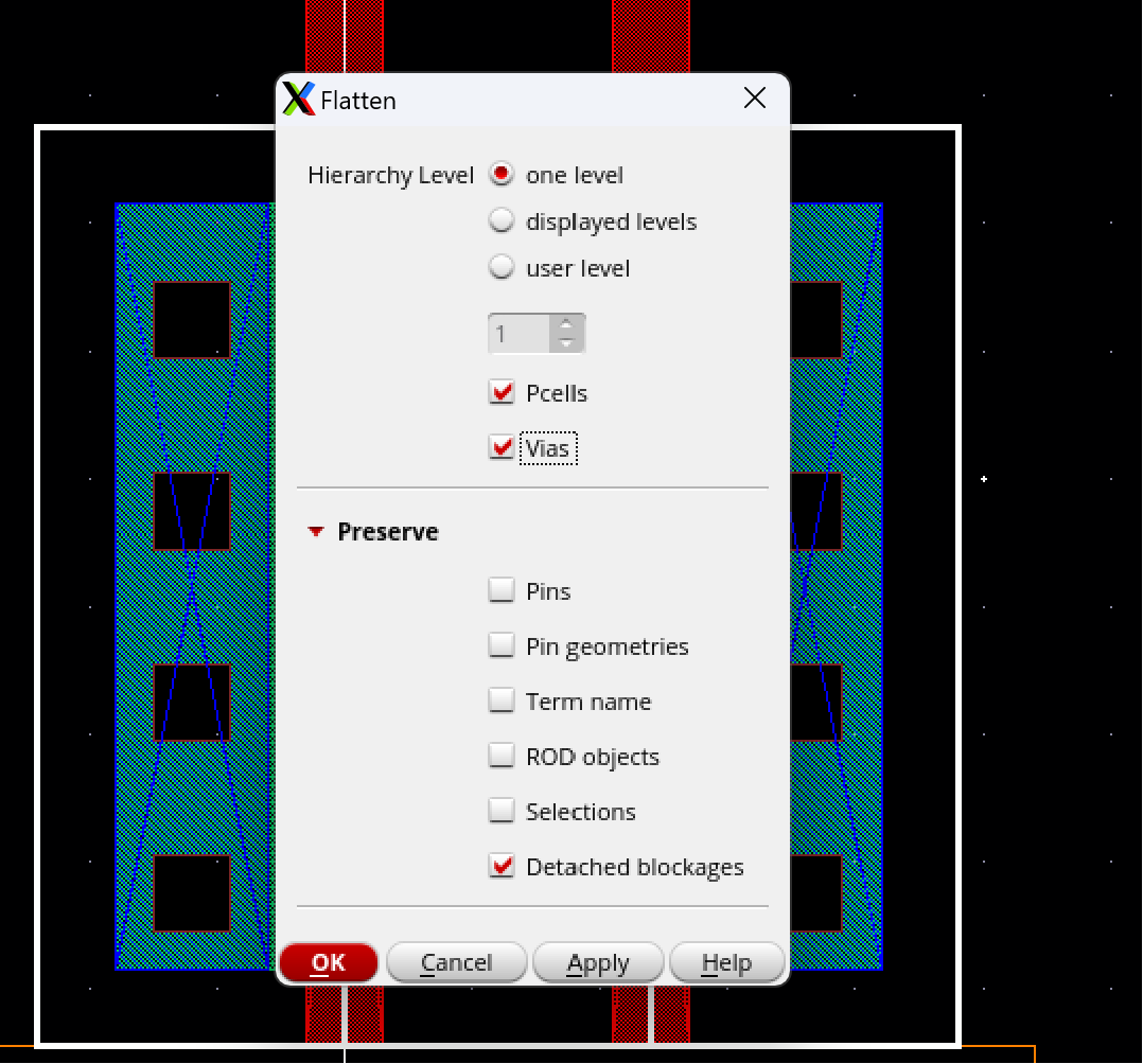
In
this next step, we dont need the middle pin so we will flatten the two
NMOS so that they are placed as if we drew them (i.e as
rectangles).
Select
both NMOS and navigate to Edit -> Herarchy -> Flatten and
de-select Preserve Pins Geometries, and make sure that Pcells are
checked:
After
we flatten, we can now delete the middle contacts and metals so that
only the active layer is visible as seen in the following images.
We
will then add the metal1 connections for the NAND gate. Also, add the
pin for AnandB which will be the output pin of the NAND gate.
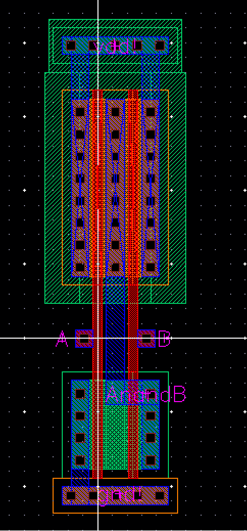
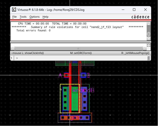
At this point our layout is basically complete, heres the DRC pass for this created layout:
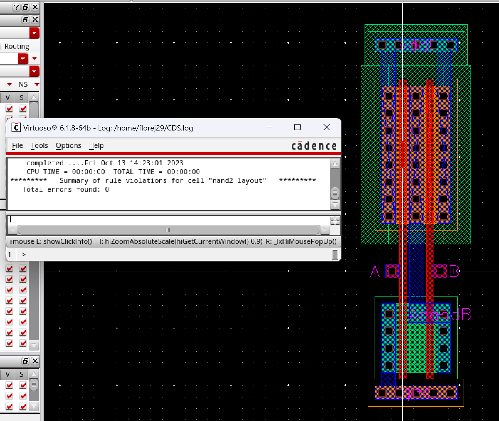
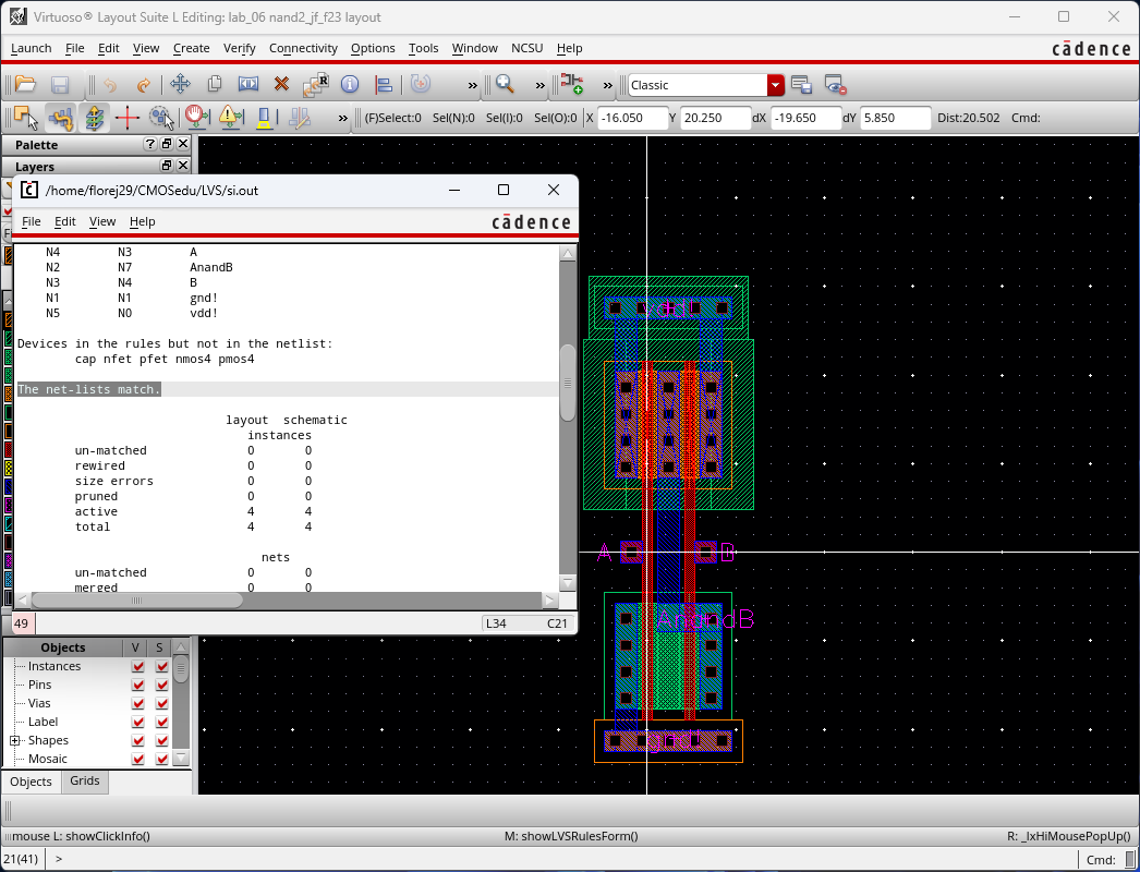
Running the LVS right after extracting:
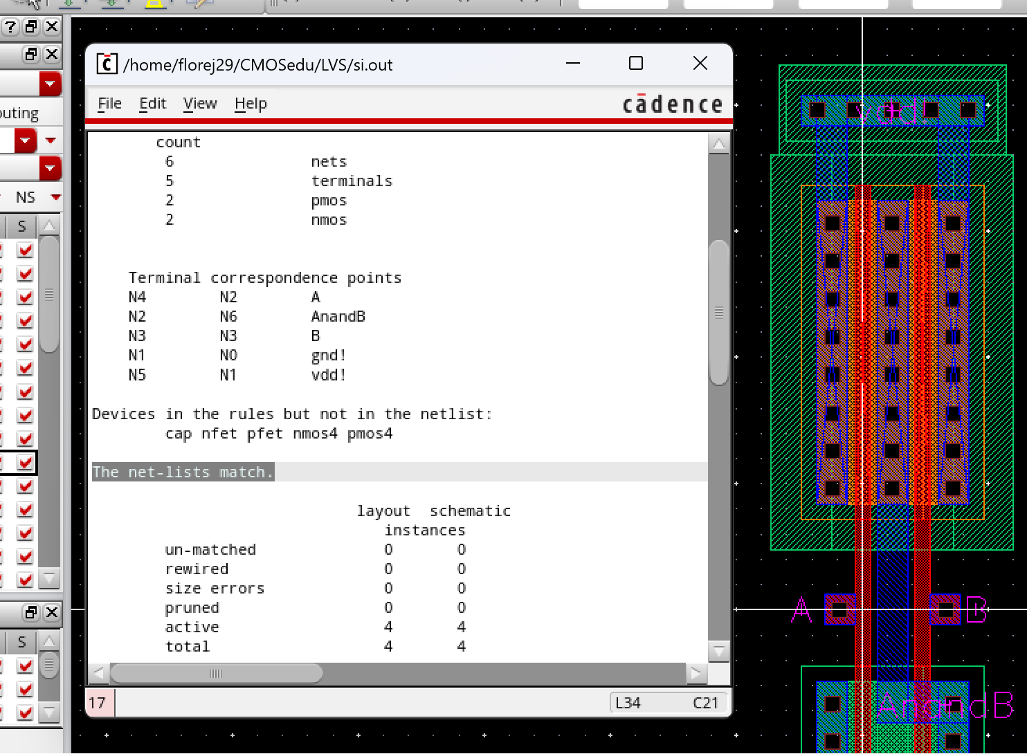
But
now we have to show that thye dont match due to the size of the PMOS in
the layout is not the same size as in the schematic. So in the Layout
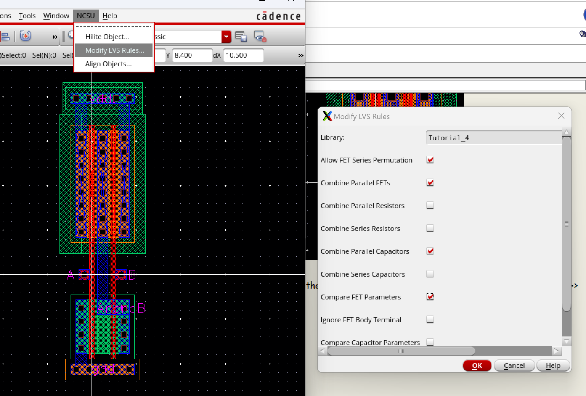
window, navigate to NCSU -> Modifu LVS Rules and check Compare FET
Parameters.
Lab Objectives
- Draft
the schematics of a 2-input NAND gate (Fig. 12.1), and a 2-input XOR
gate (Fig. 12.18) using 6u/0.6u MOSFETs (both NMOS and PMOS)
- Create layout and symbol views for these gates showing that the cells DRC and LVS without errors
- ensure
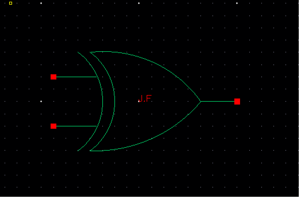
that your symbol views are the commonly used symbols (not boxes!) for
these gates with your initials in the middle of the symbol
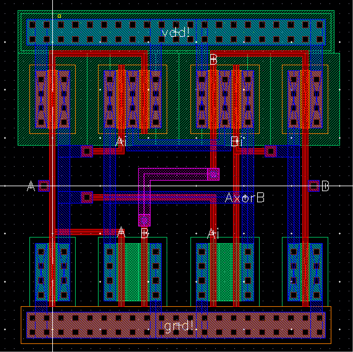
- ensure all layouts in this lab use standard cell frames that snap together end-to-end for routing vdd! and gnd!
- use a standard cell height taller than you need for these gates so that it can be used for more complicated layouts in the future
- ensure gate inputs, outputs, vdd!, and gnd! are all routed on metal1
- Use cell names that include your initials and the current year/semester, e.g. NAND_jb_f29 (if it were fall 2029)
- Using Spectre simulate the logical operation of the gates for all 4 possible inputs (00, 01, 10, and 11)
- comment on how timing of the input pulses can cause glitches in the output of a gate
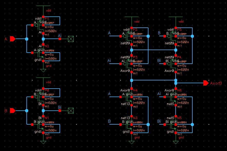
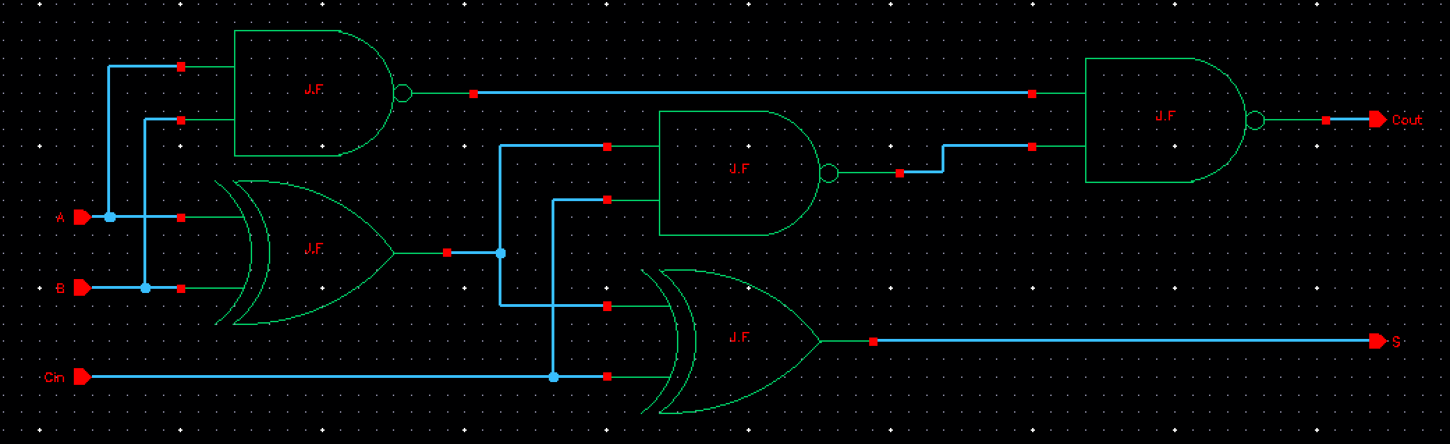
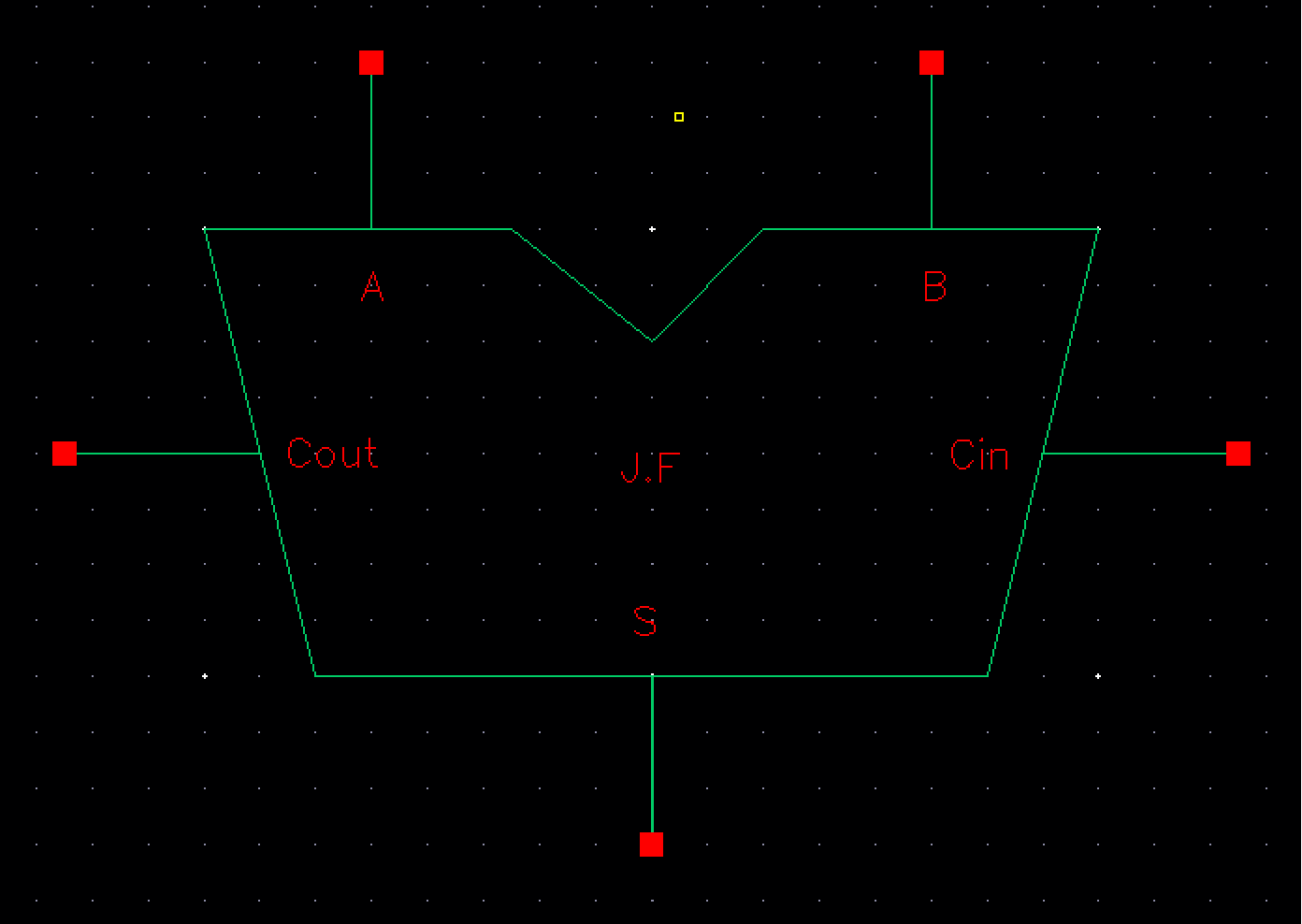
- Using these gates, draft the schematic of the full adder seen below
- Create a symbol for this full-adder
- Simulate, using Spectre, the operation of the full-adder using this symbol
- Layout the full-adder by placing the 5 gates end-to-end so that vdd! and gnd! are routed
- full-adder inputs and outputs can be on metal2 but not metal3
- DRC and LVS your full adder design
Lab
NAND Gate
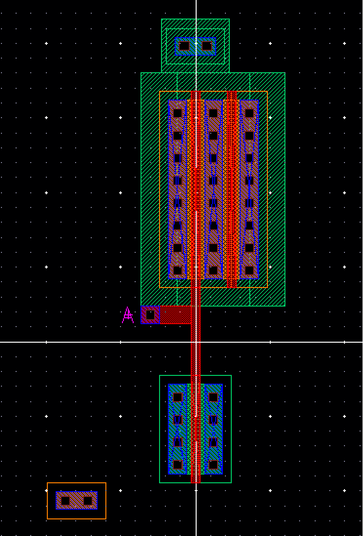
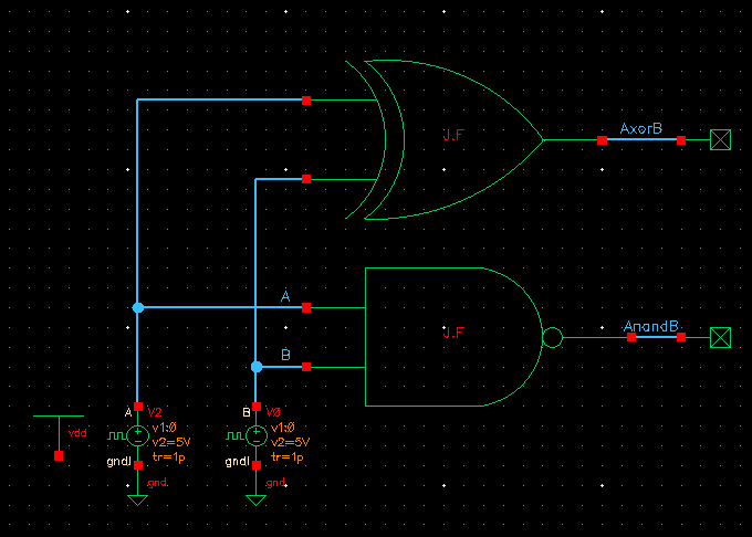
Below you will find the schematic, symbol and layout of the 2-input NAND gate.
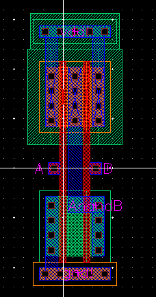
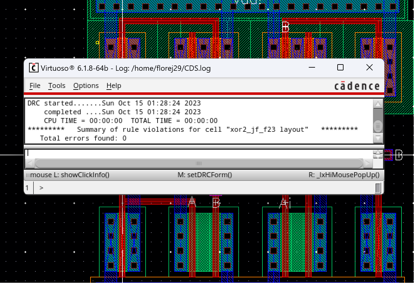
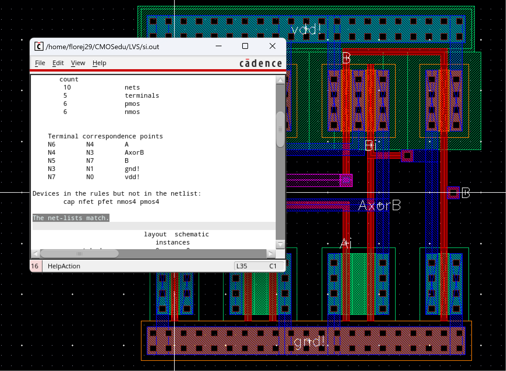
Layout DRC and LVS of NAND gate:
XOR Gate
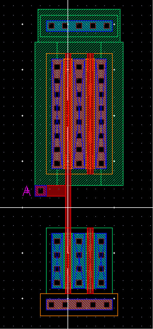
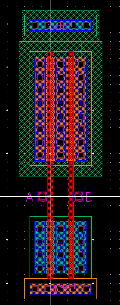
Below you will find the schematic, symbol and layout of the 2-input XOR gate.
Layout DRC and LVS of XOR gate:
Simulation of Both NAND and XOR Gates
Below
you will find the simulations for both the NAND and XOR gate
operations. Note that both gates were used at the same time to
demonstrate their operation in one simulation.
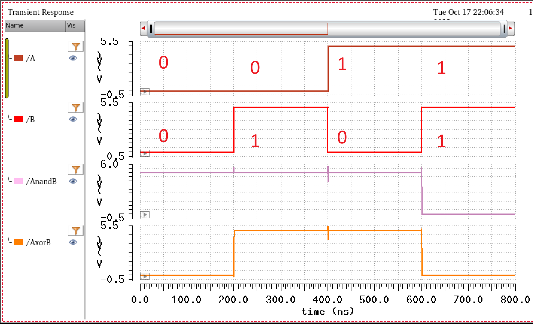
These
glitches that are seen above are cuased by the sudden change in our
input signals as seen in the simulation. This brief moment causes are
MOSFETS to neither on or off, and therefore causing these sudden
spikes. If we were to ideally have the rise and fall time to be 0,
these spikes would never apear.
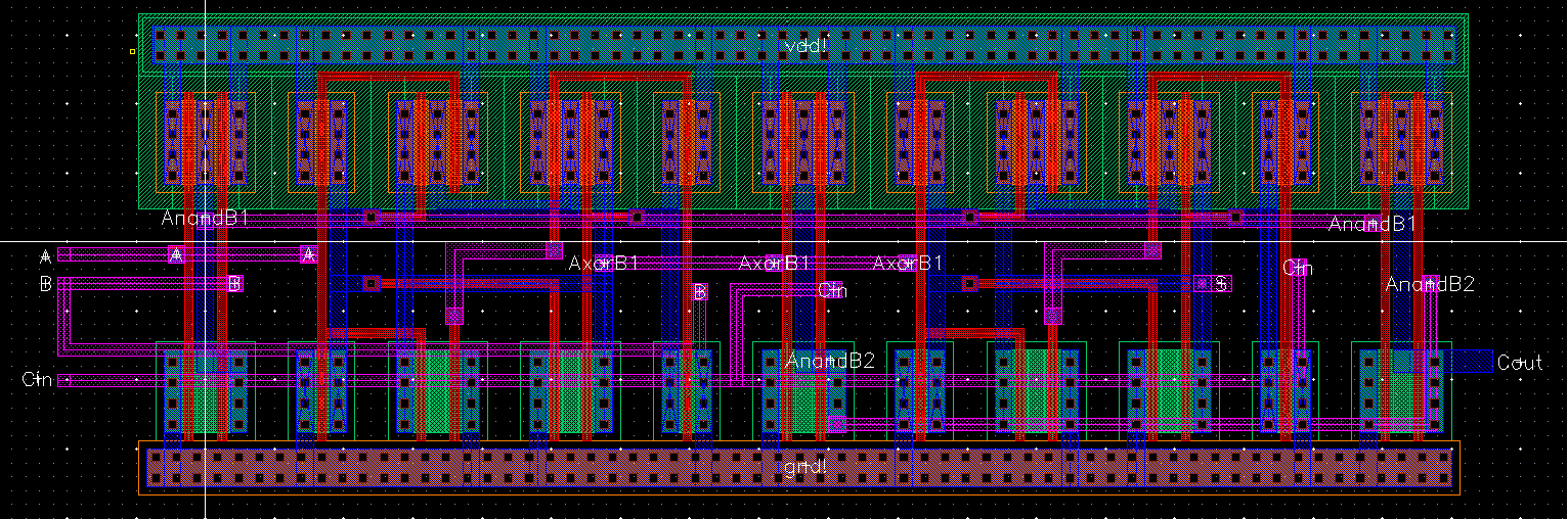
Full Adder
Schematic, Symbol, and Layout of the full adder:
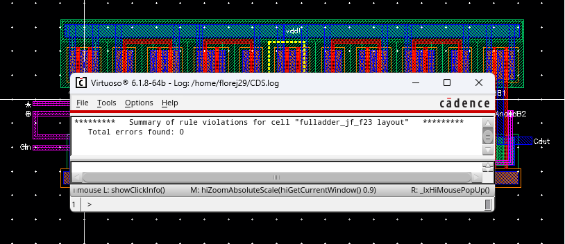
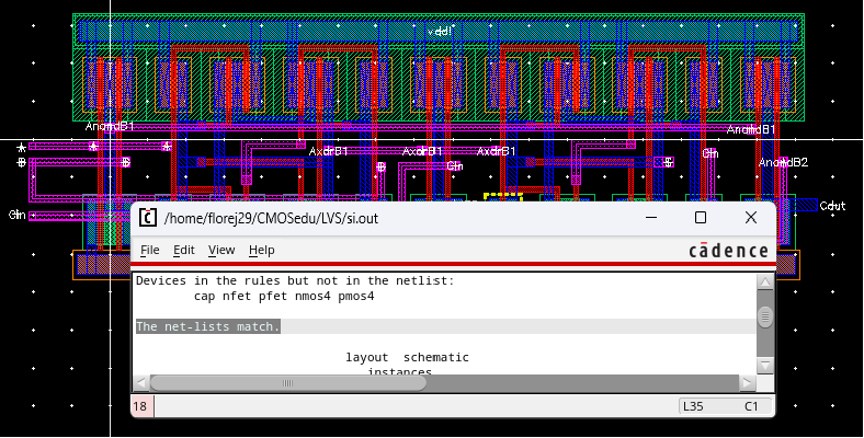
DRC and LVS of Full Adder:
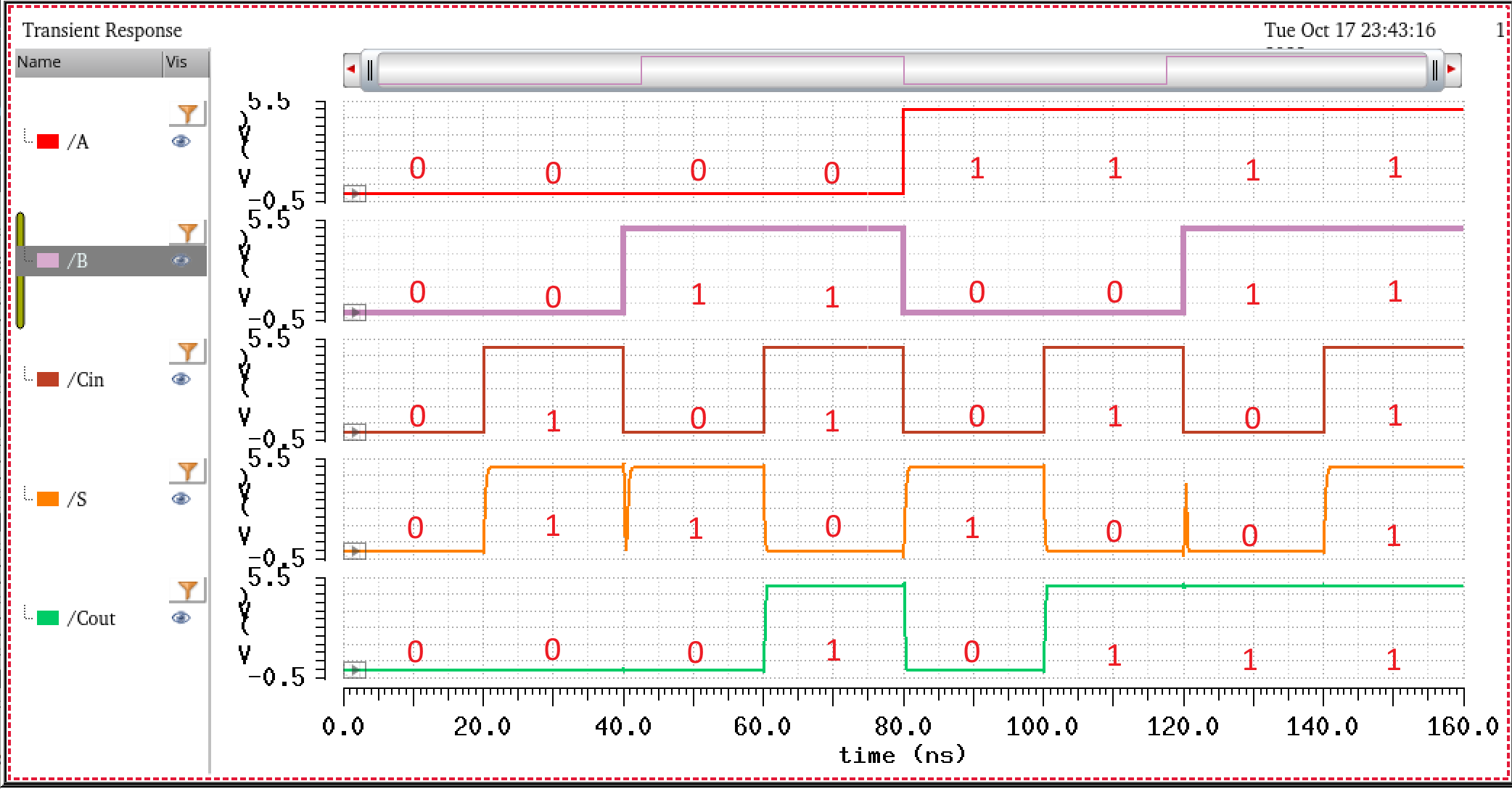
Simulation of Full Adder
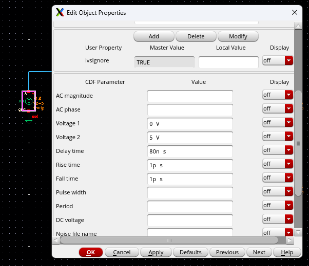
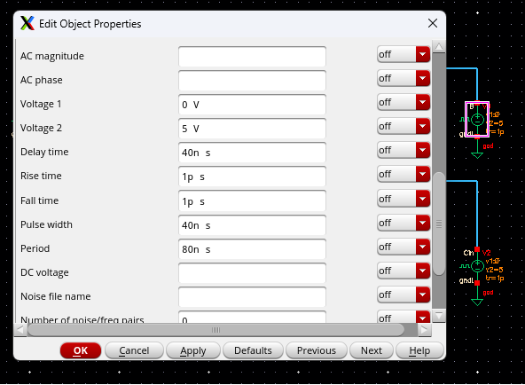
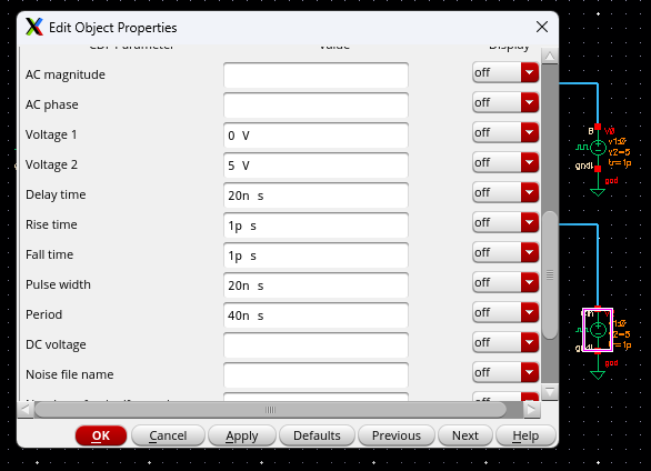
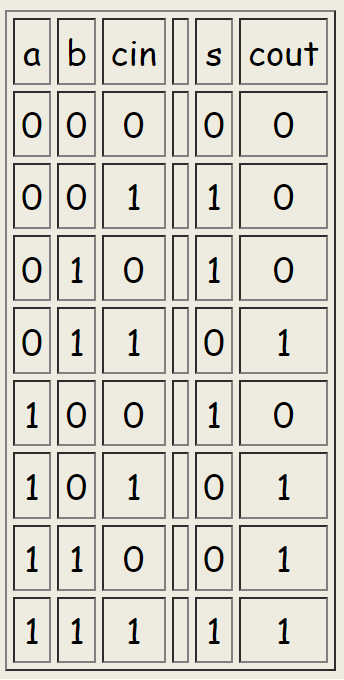
Here's
the simulation of the full adder. Note that each input has different
periods in order to obtain the desired inputs at a desired time, to get
our truth table values in order. In other words for input A, I gave a
80ns delay, and left it on for the remaining time period. Input B
has a 40ns delay, with a period of 80ns. Finally input Cin, has 20ns
delay, with a 40ns period. This yields the results matching the truth
table.
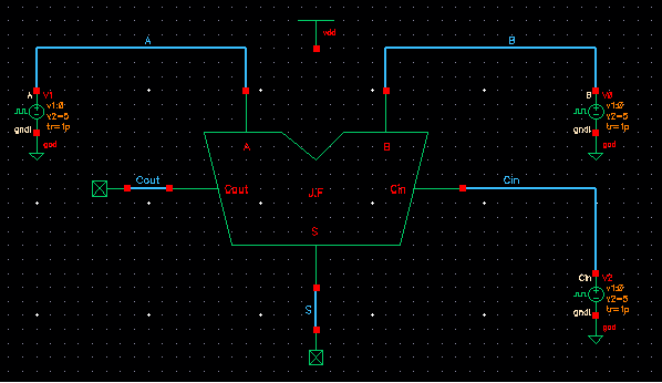
Pulse Source Settings used for A, B, and Cin, respectively:
This concludes the end of Lab 6. Below you can find this labs zip file with the all the files used in this lab.
>> Lab 7 <<
Return to florej29 Lab Reports
Return to Fall 2023 EE421L Student Lab Reports
Return to Fall 2023 Digital Integrated Circuit Design Laboratory Home Page