Lab 5 -
EE 421L
Authored
by Jesus Flores-Arellano
Email:
florej29@unlv.nevada.edu
October
10, 2023
Lab
description
-Design, layout, and
simulation of a CMOS inverter
Prelab
Tasks
-
Go through Tutorial 3
Prelab
To
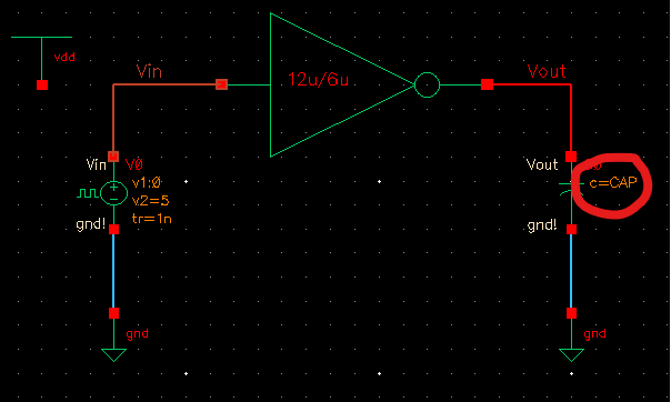
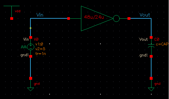
start off this prelab, we made the schamatic of an inverter using a
6u/6n (W/L) NMOS and (12u/6n) PMOS connected as seen
in the
shematic below:
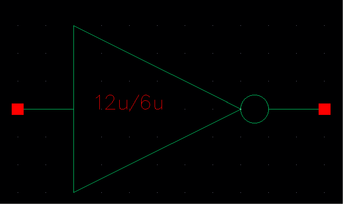
We
then also make the symbol view:
Following
the schematic and symbol view of the inverter, we proceed to the
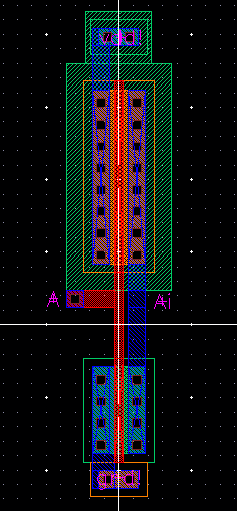
layout. We instantiate an NMOS and PMOS with the same specifications as
above, a m1_poly to connect our polys layers, ntap for the PMOS Vdd
connection, and ptap for the NMOS ground connection. We then connect
them with metal1 layer, and assign the pin assignment accordingly,
while not forgetting that the left pin is an input pin, and right pin
is the output pin, ntap and ptap pin is assigned as input/output. This
step is importnat for the LVS process. We then get the following:
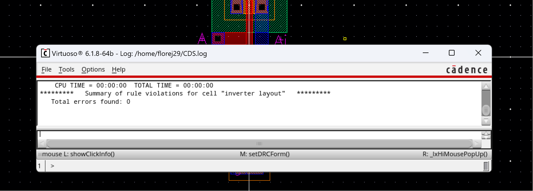
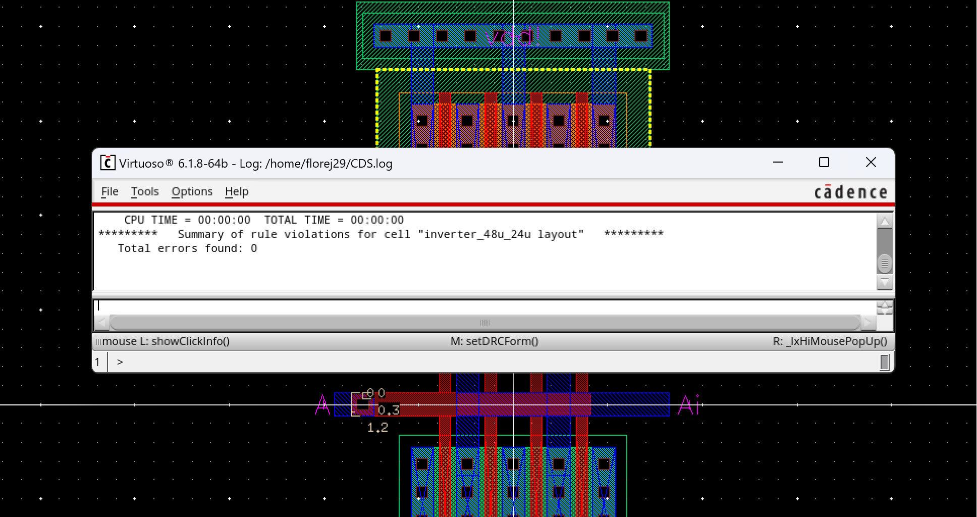
We then DRC our layout
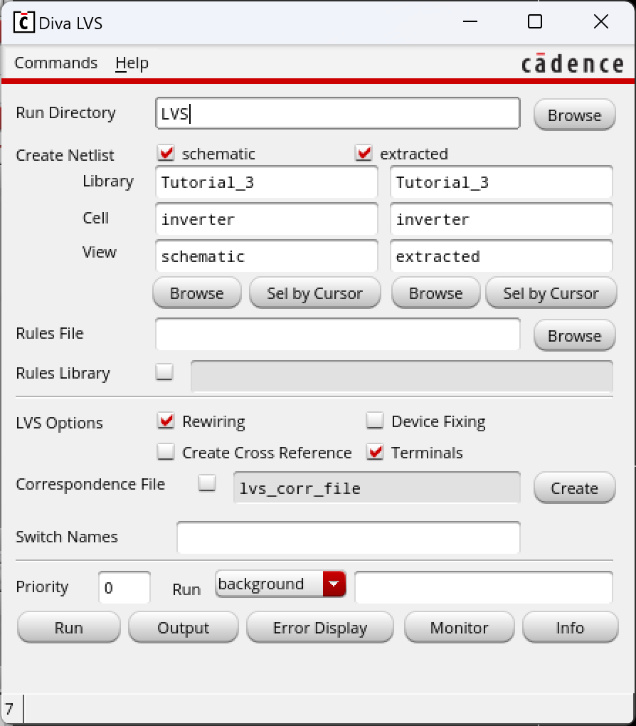
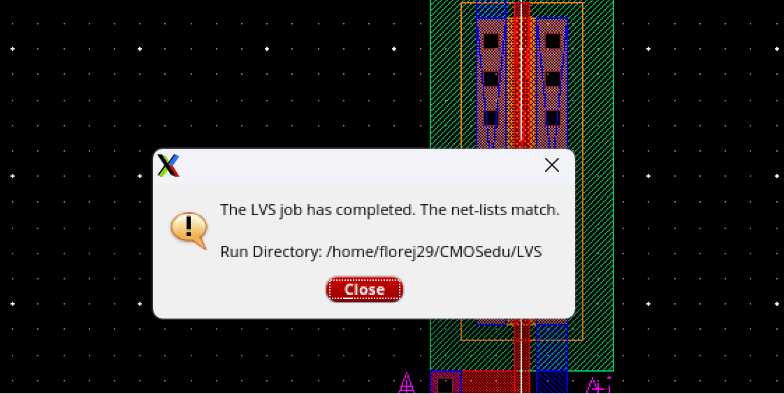
Now that we have a clean DRC, we can LVS our layout and schematic,
results are seen below:
End of prelab, Tutorial 3.
Lab Objectives
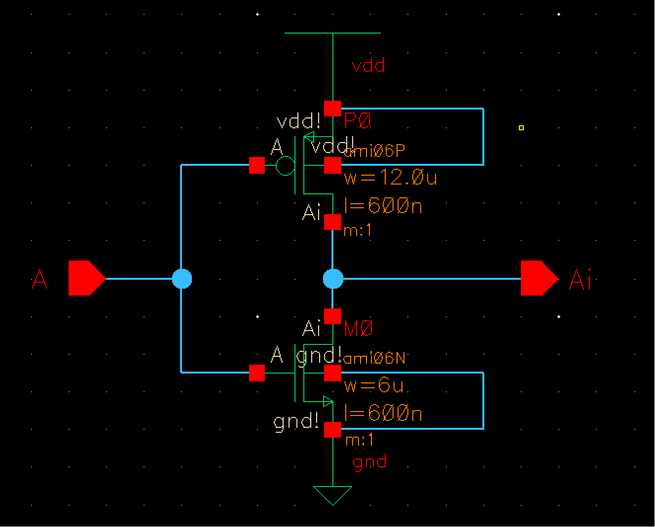
- Draft
schematics, layouts, and symbols for two inverters having sizes
of:
- 12u/6u
(= width of the PMOS / width of the NMOS with both devices having
minimum lengths of 0.6u)
- 48u/24u
where the devices use a multiplier, M = 4 (set along with the width and
length of the MOSFET, image), as seen below
- Using
SPICE simulate the operation of both of your inverters showing each
driving a 100 fF, 1 pF, 10 pF, and 100 pF capacitive load
- Comment,
in your report, on the results
- Use UltraSim (Cadence's fast SPICE simulator for larger
circuits at the cost of accuracy) and repeat the above
simulations
- Use Setup -> Simulator/Directory/Host and select
UltraSim as seen below
- You'll also have to point to the MOSFET models again as
seen below
- Note that UltraSim only performs transient simulations
(not AC,
Noise, DC, operating point, etc.)
- Not knowing this last item will lead to wasted time if
trying to use UltraSim exclusively for simulations
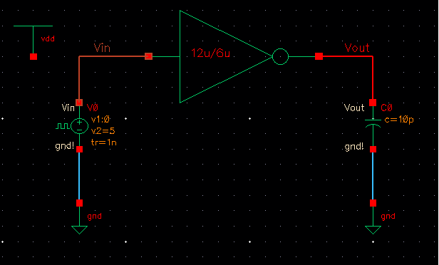
Lab
12u/6u
Inverter
Schematics
of 12u width of the PMOS & 6u width of the NMOS with both
devices
having minimum lengths of 0.6u, are can be seen below:
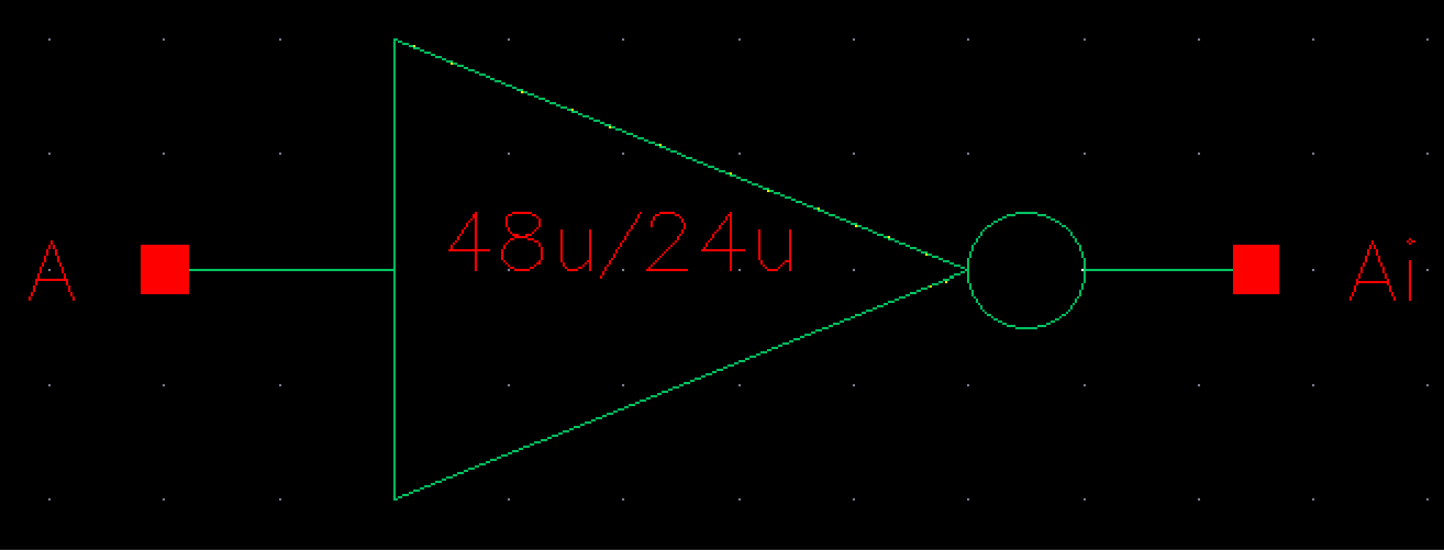
The symbol for schematic
seen above :
Layout
view:
DRC
and LVS:
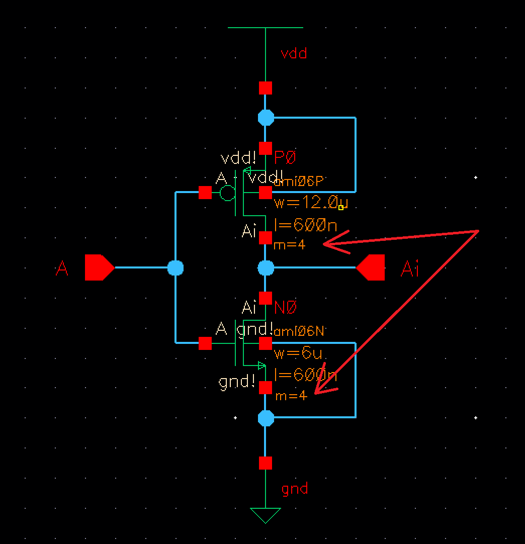
48u/24u
Inverter
Similarly,
the following process was the same , but with a multiplier of 4 ( m =
4) for the NMOS and PMOS, which gives us a 48u/6n, 24u/6n, PMOS and
NMOS, respectively.
You
will find the schematic, and Symbol view in the images below.
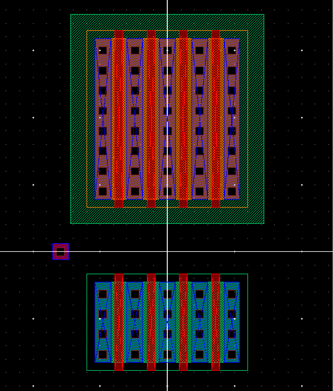
For
the layout we can start by instantiating a 12u/6n PMOS and 6u/6n NMOS
and both with multipliers of 4 (i.e m = 4) as seeen below. This will
obviously give us the desired value of our 48u/24u Inverter.
After,
we layout the metal1, poly, and pin connections as per our schematic.
We should end up with the following below:
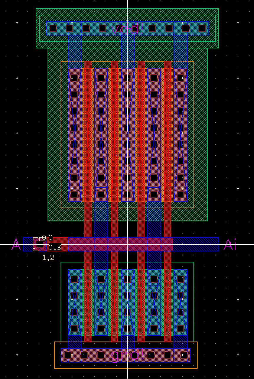
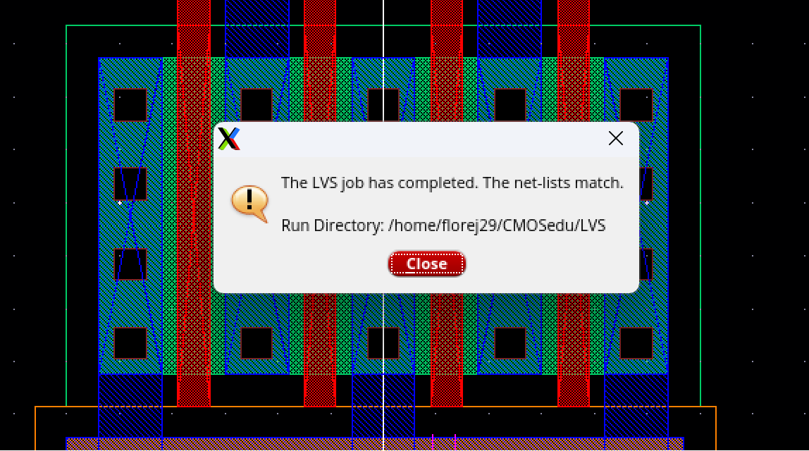
DRC
pass for the finished layout:
Once
we pass the DRC, we can LVS now:
Now
that we have both Inverters done (i.e 12u/6u and 48u/23u ) we can move
onto the simulations.
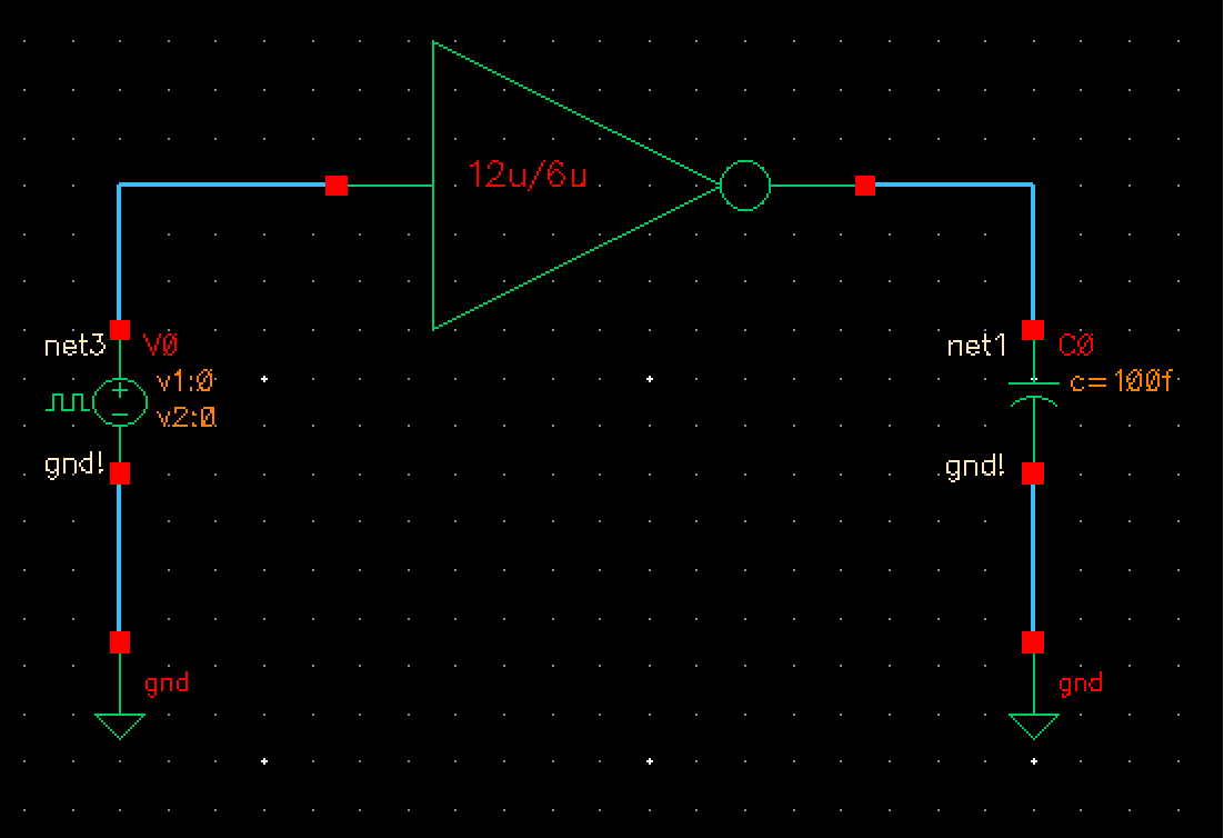
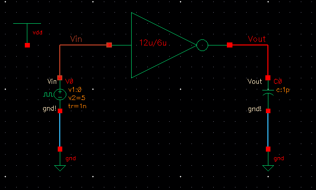
Simulations
For
these next simulations, the inverters will be driving a 100fF, 1pF,
10pF, and 100pF capacitive load.
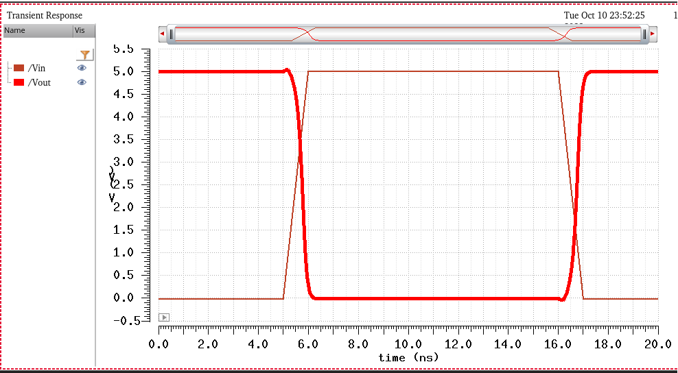
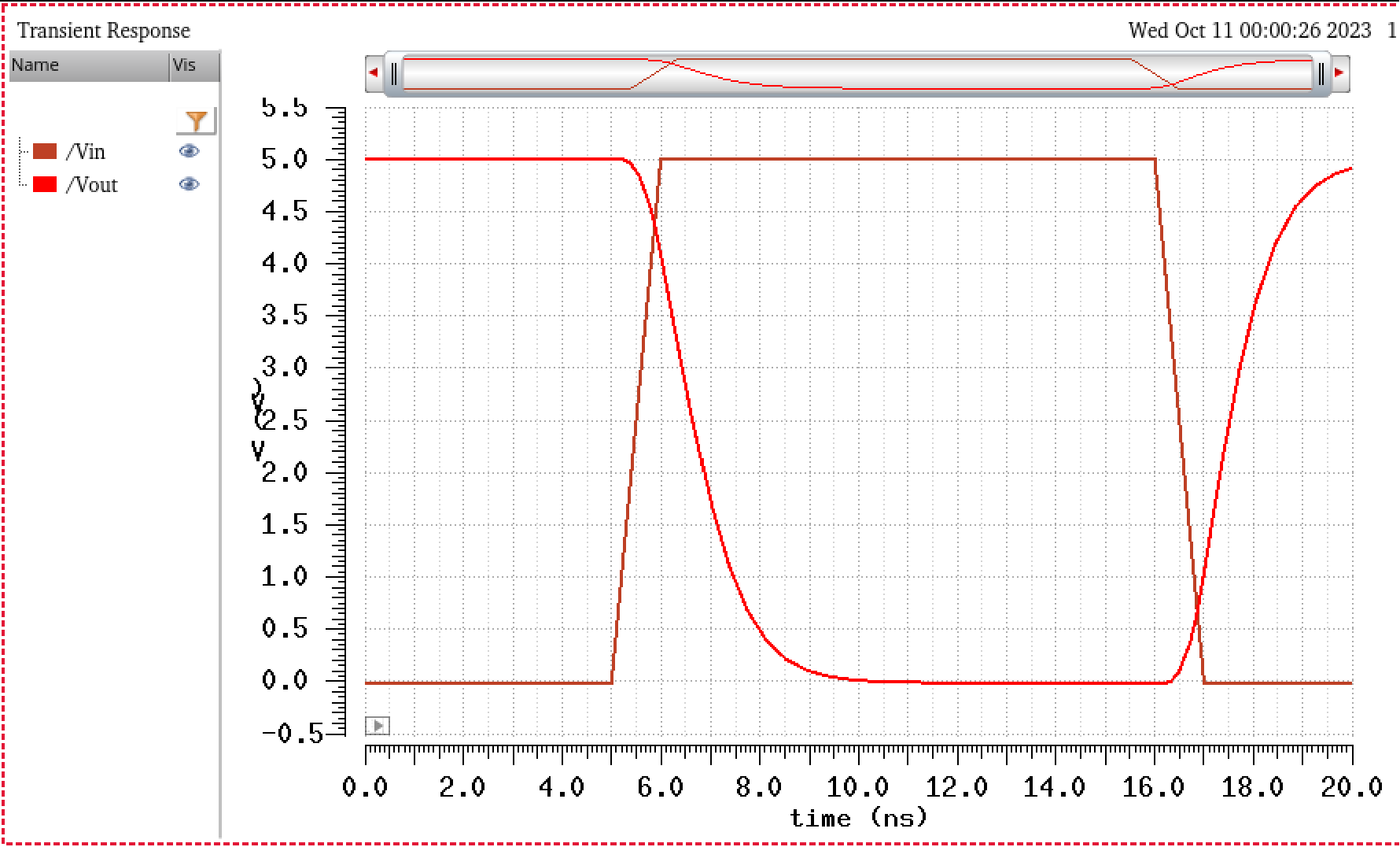
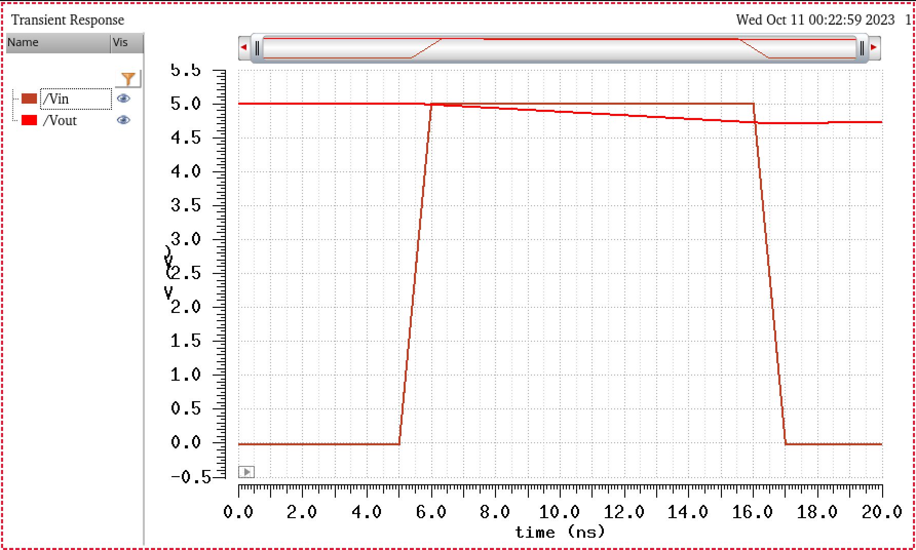
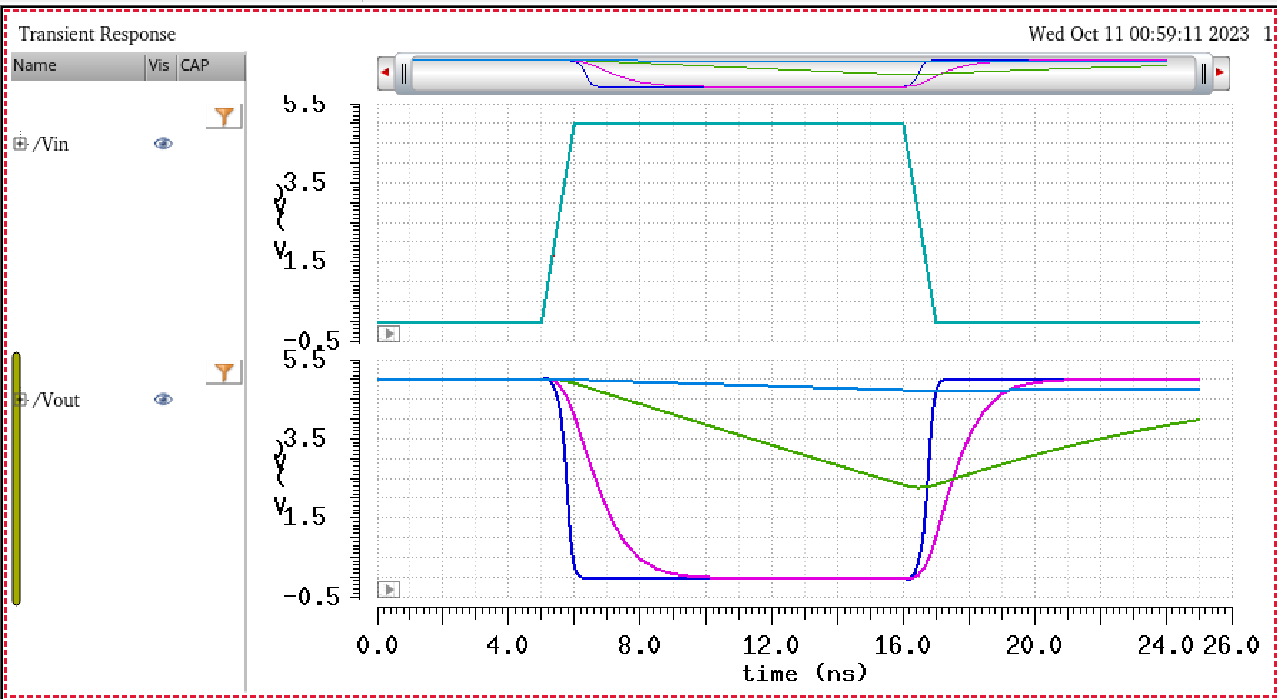
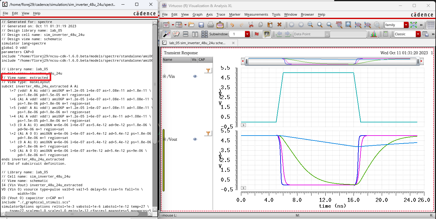
For
the following simulation below , we can observe there to be slightly
sharp edges that are in the Vout waveform. We will keep in this mind
for when we change the capcaitive load.
In
the following simulation we can analyze that the wavceform
for
Vout is smoother at one end of the graph while the other end is
slightly sharper.
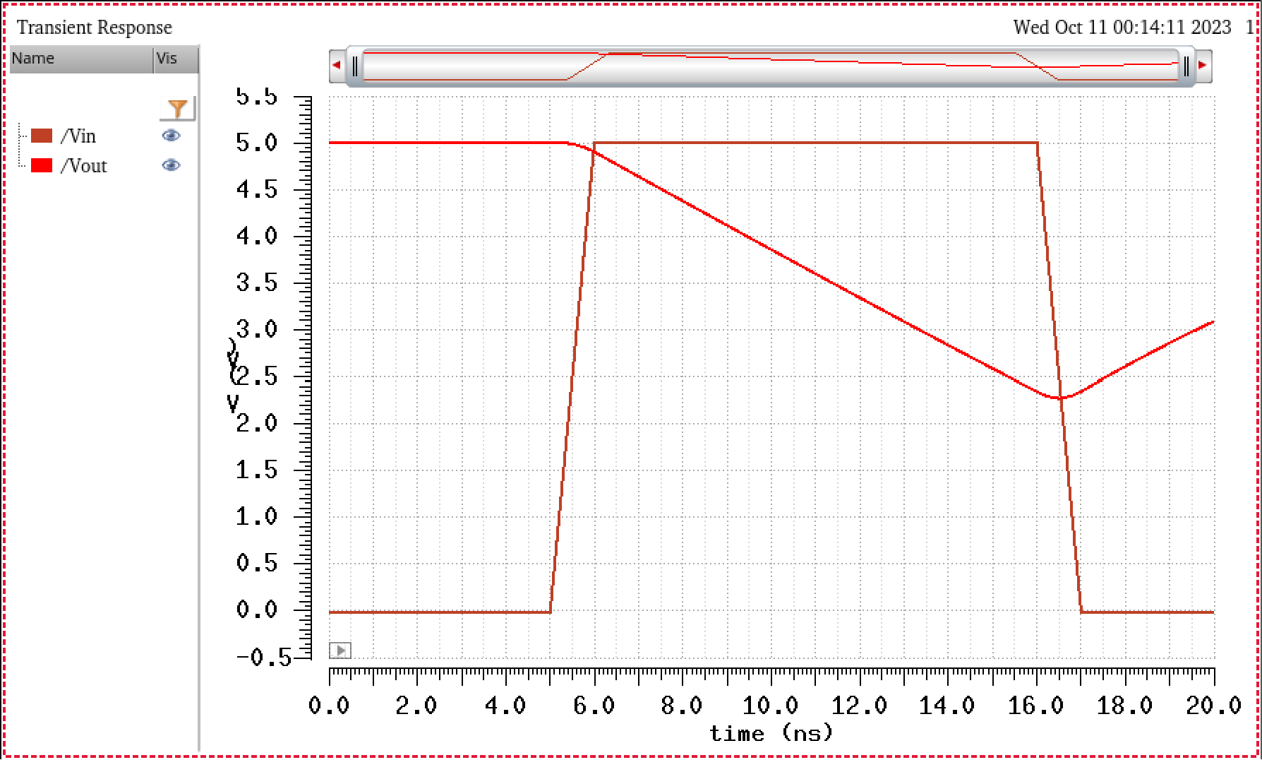
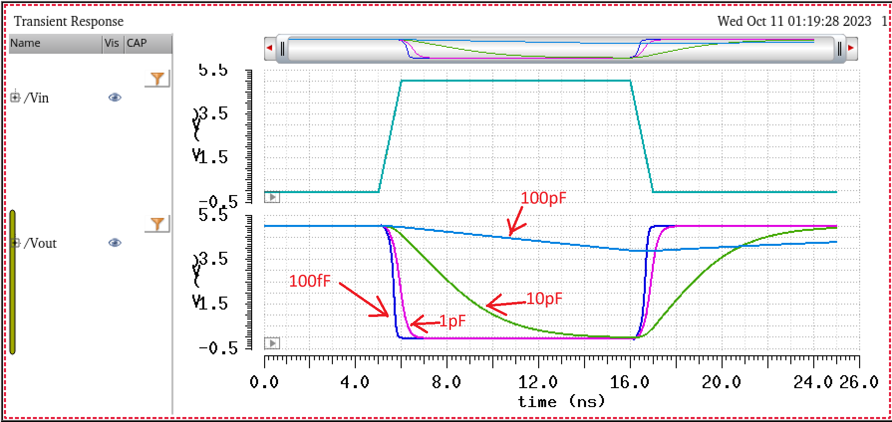
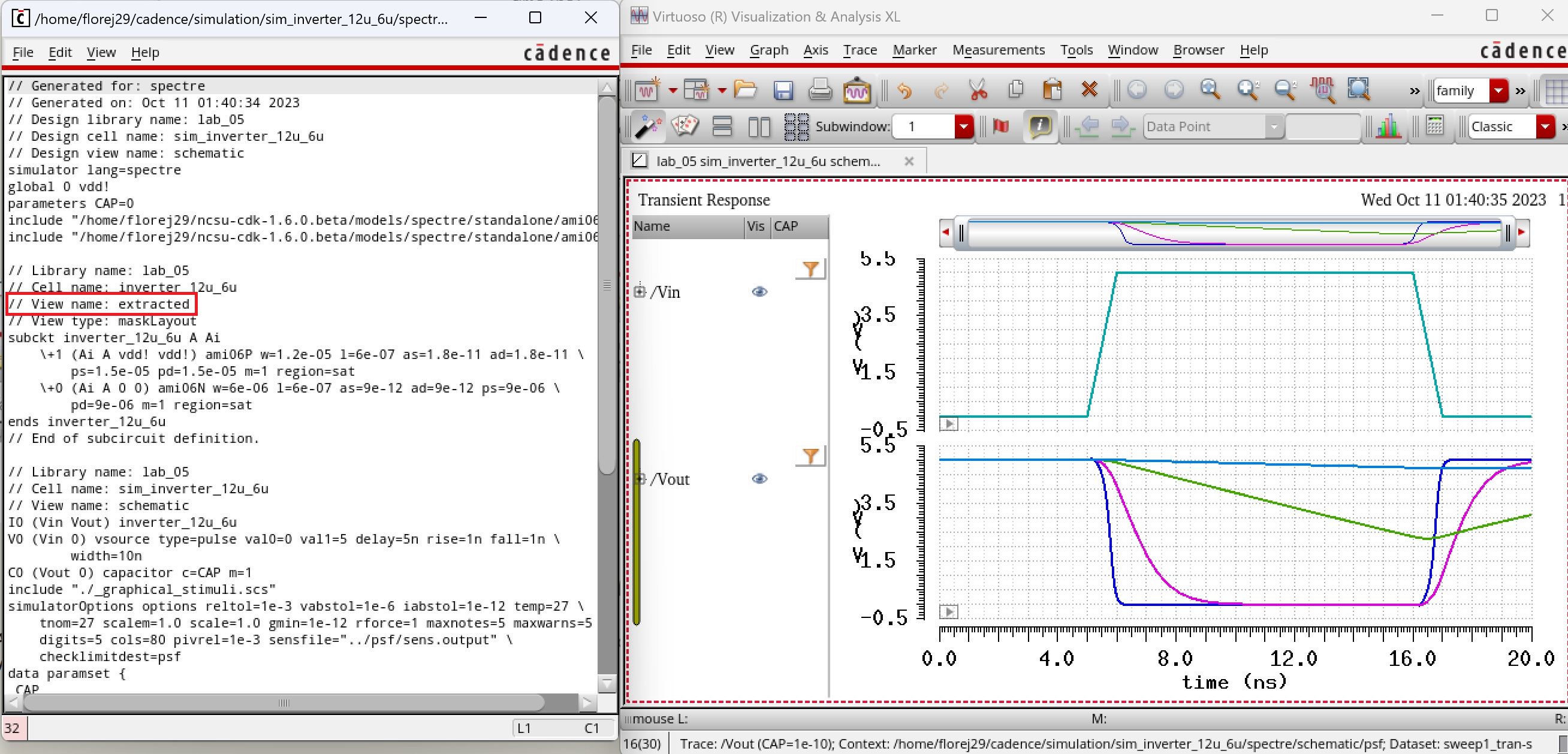
During this next
simulation, we will see that that Vout is taking a longer time to reach
the desired value of the inverter.
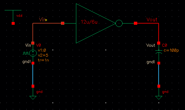
Here
we can see that the pattern continues as the previous results. At this
point the output just follows the input of the inverter, rather than
giving the inverse value.
In
sumamry, I will provide all simulations in a single graph to compare
all capacitive load situations (i.e 100fF, 1pF, 10pF, 100pF). A small
little walk through for my reference will be provided below.
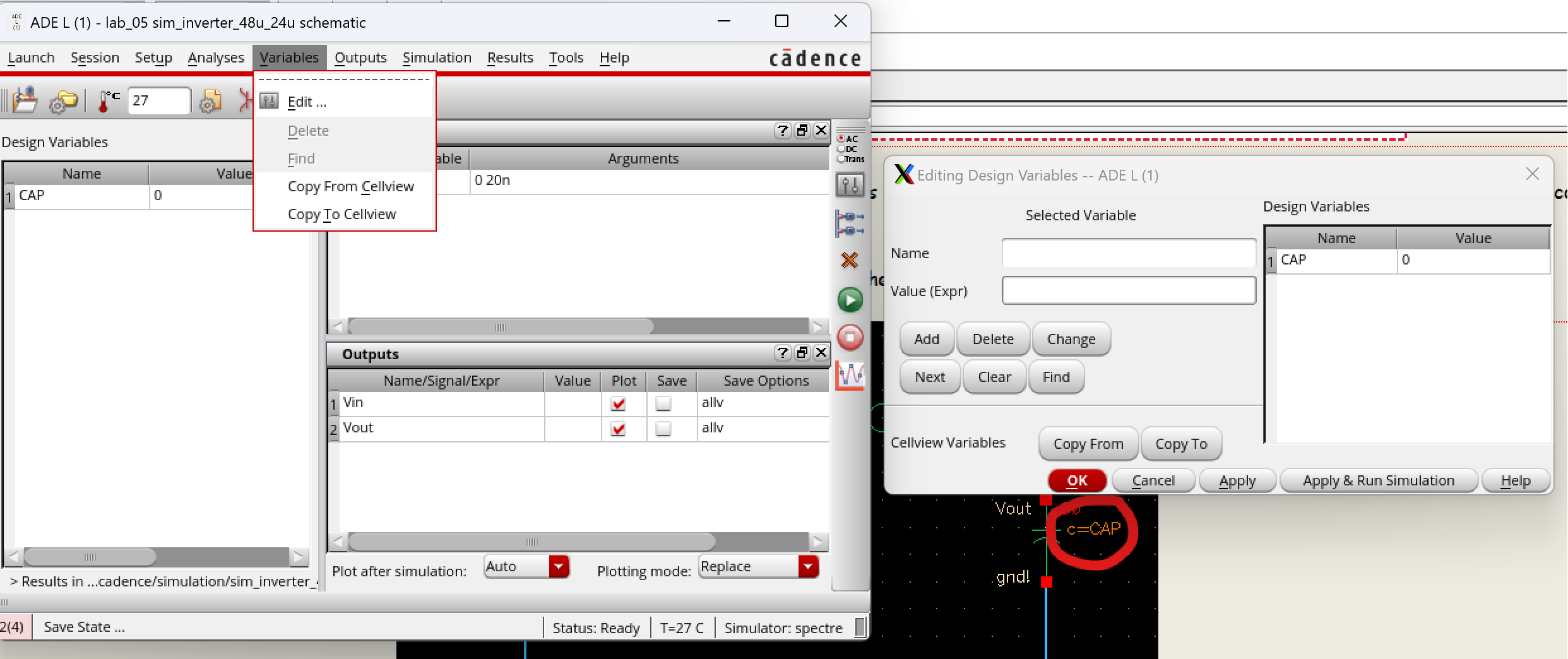
Let us define the capacitors' value as a variable, since this will be
the value we want to change in the transient simulation.
We
then define this variable the ADE L window. Go to Variables ->
Edit,
and then add the name of the variable, in this case "CAP", we can set
the value expression to 0. Click Ok.
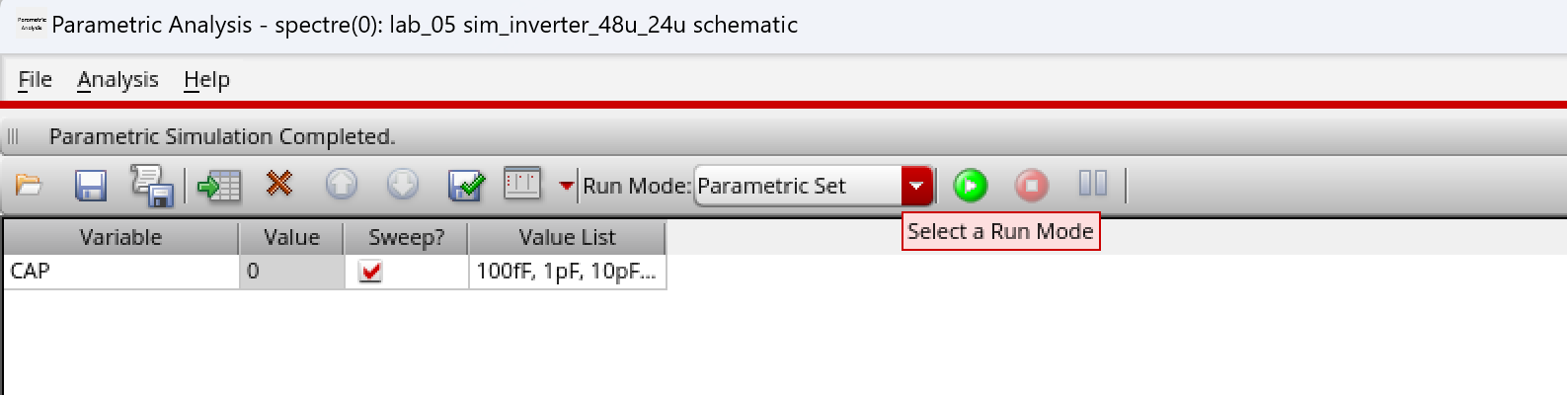
Assuming
we have everything else setup for simulation, we can then go to Tools
-> Parametric Analysis, Change Run Mode to Parametric Set, Add
the
variable "Cap" and add the list of values that we want as seen below:
We can then run the simulation with the green play button
next to Parametric Set.
48u/24u
Inverter Simulation
I will
do the same procedure to simulate the 48u/24u inverter to save time and
less pictures.
All combination for the capacitive loads will be given in the
simulation below:
As
we can see, with the inverter with a higher multiplier, or more
MOSFETs, allows the capacitor to more effeciently charge and
discharge.
Extracted
Simulation of 48/24u , 12u/6u, Inverters respectively.
This wraps up Lab 5. You can find my lab 5 files in the zipped folder
below.
>> Lab 5
<<
Return
to florej29 Lab Reports
Return
to Fall 2023 EE421L Student Lab Reports
Return
to Fall 2023 Digital Integrated Circuit Design Laboratory Home Page