Lab 4 -
EE 421L
Authored
by Jesus Flores-Arellano
Email:
florej29@unlv.nevada.edu
September
27, 2023
Lab
description
-
During this lab we will layout and simulate the operation of an NMOS
and PMOS transistor, using a C5 process. We will also finish up
tutorial 2 for the pre-lab.
Prelab
Tasks
-
Finish up Tutorial 2 and upload images layouts and simulations.
Prelab
For
this prelab we finished up Tutorial 2.
We
first created a schematic cell, drew out a circuit and simulated it to
view a ID vs VGS graph using an NMOS transistor as seen below in the
following images.
Schematic Circuit with our created NMOS symbol:
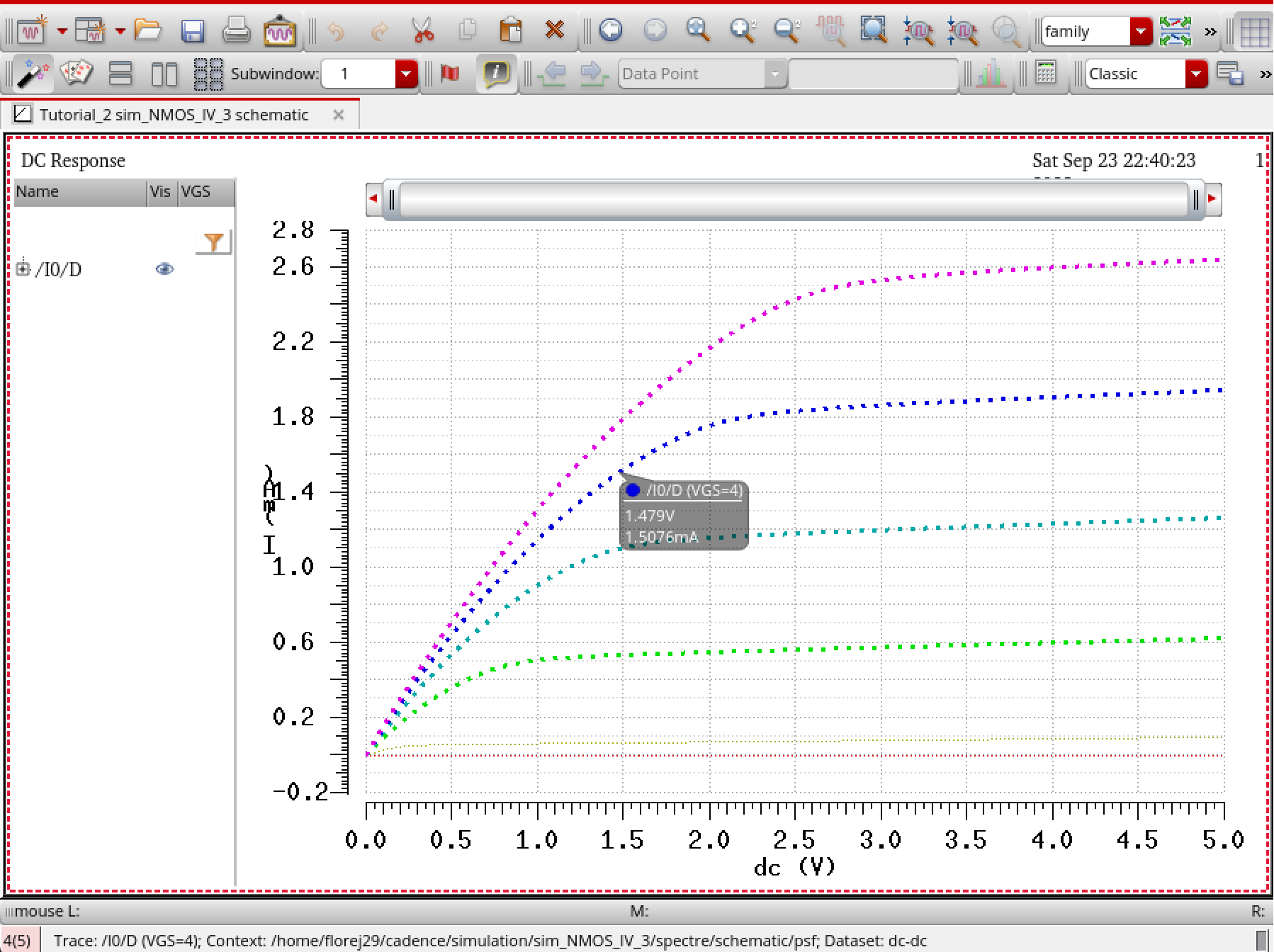
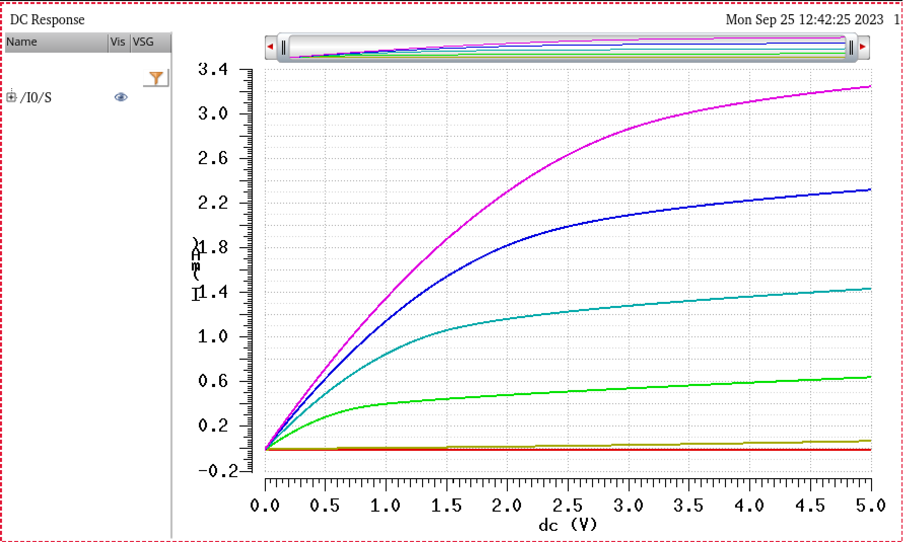
Simulation graphs of NMOS (ID vs VGS) with varying VGS :
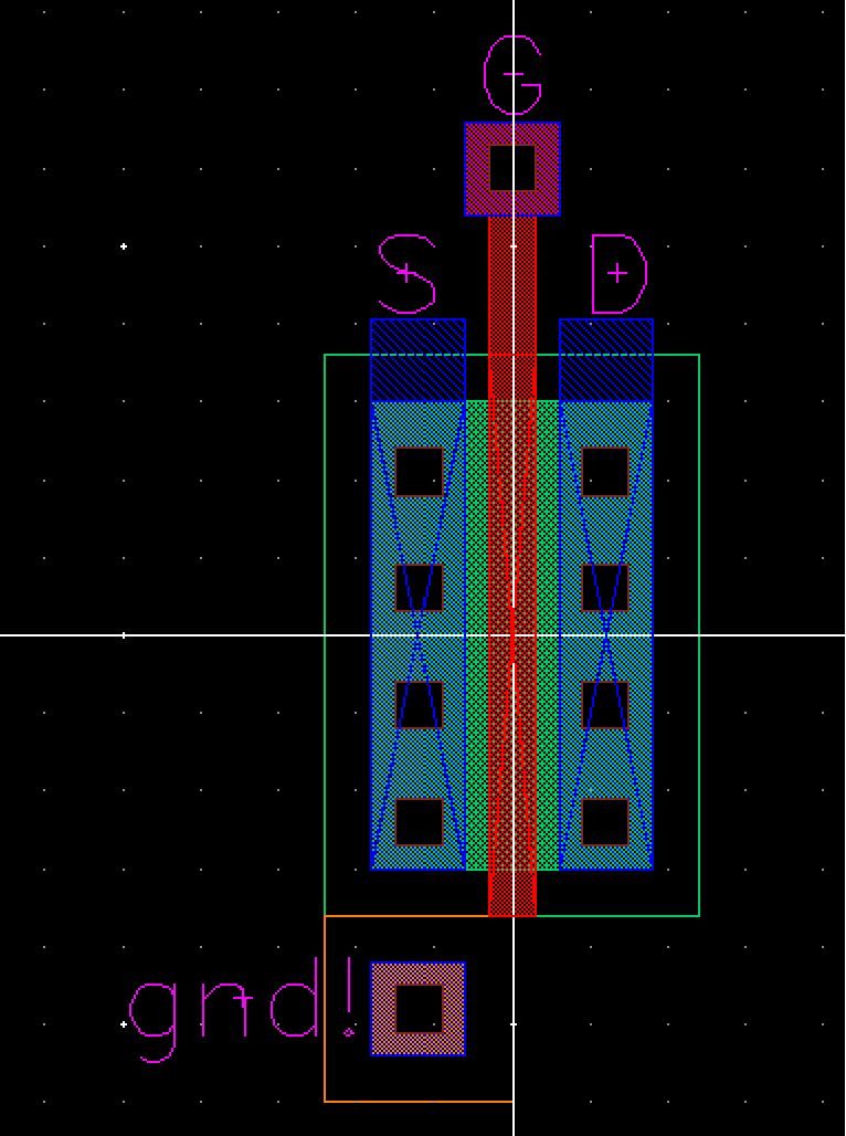
Layout of created NMOS:
Once finished with the NMOS walk through of the tutorial, we simoly
repeated all the same steps for the PMOS transistor now.
Schematic circuit with our created PMOS Symbol:
Simulation graphs (ID vs VSG) with varying VSG:
Layout view of creaetd PMOS:
Once both NMOS and PMOS layouts are created, the Tutorial is condluded.
Lab Objectives
- Generate
4 schematics and simulations (see the examples in the Ch6_IC61 library,
but note that for the PMOS body should be at vdd! instead of gnd!):
- A
schematic for simulating ID
v. VDS of an NMOS device for VGS varying from 0 to 5 V in 1 V steps
while VDS varies from 0 to 5 V in 1 mV steps. Use a 6u/600n
width-to-length ratio.
- A
schematic for simulating ID v. VGS of an NMOS device for VDS = 100 mV
where VGS varies from 0 to 2 V in 1 mV steps. Again use a 6u/600n
width-to-length ratio.
- A
schematic for simulating ID v. VSD (note VSD not VDS) of a PMOS device
for VSG (not VGS) varying from 0 to 5 V in 1 V steps while VSD varies
from 0 to 5 V in 1 mV steps. Use a 12u/600n
width-to-length ratio.
- A
schematic for simulating ID v. VSG of a PMOS device for VSD = 100 mV
where VSG varies from 0 to 2 V in 1 mV steps. Again, use a 12u/600n
width-to-length ratio.
- Lay
out a 6u/0.6u NMOS device and connect all 4 MOSFET terminals to probe
pads (which can be considerably smaller than bond pads [see MOSIS
design rules] and directly adjacent to the MOSFET
(so the layout is relative small).
- Show your
layout passes DRCs.
- Make a
corresponding schematic so you can LVS your layout.
- Lay out a
12u/0.6u PMOS device and connect all 4 MOSFET terminals to probe
pads.
- Show your
layout passes DRCs.
- Make a
corresponding schematic so you can LVS your layout.
Lab
Generating
4 Schematics and Simulations
For
the first part of the lab, we will need create 2 MOSFET schematics. We
will need to create a NMOS and PMOS transistor schematic, and simulate
each with the specified parameters listed in the lab description
above.
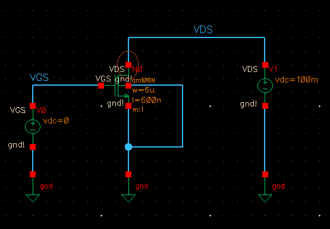
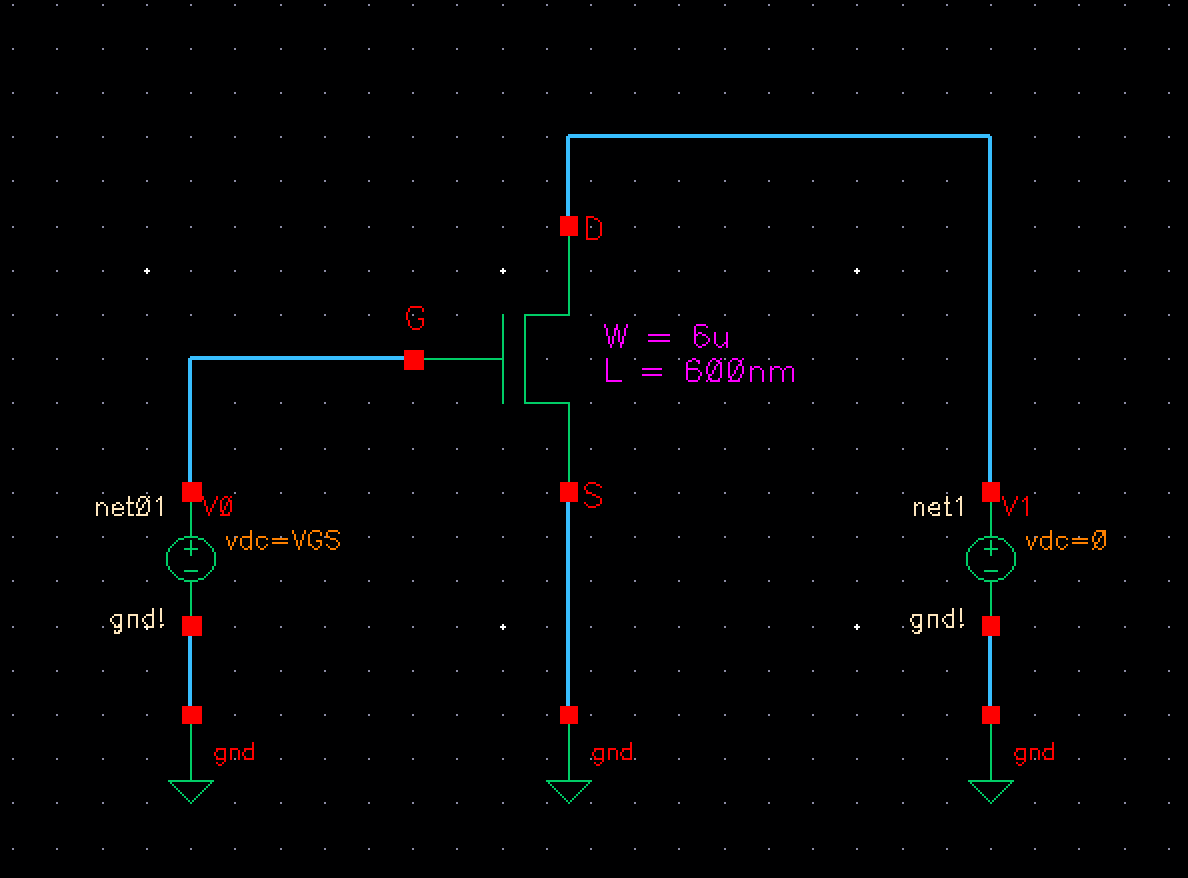
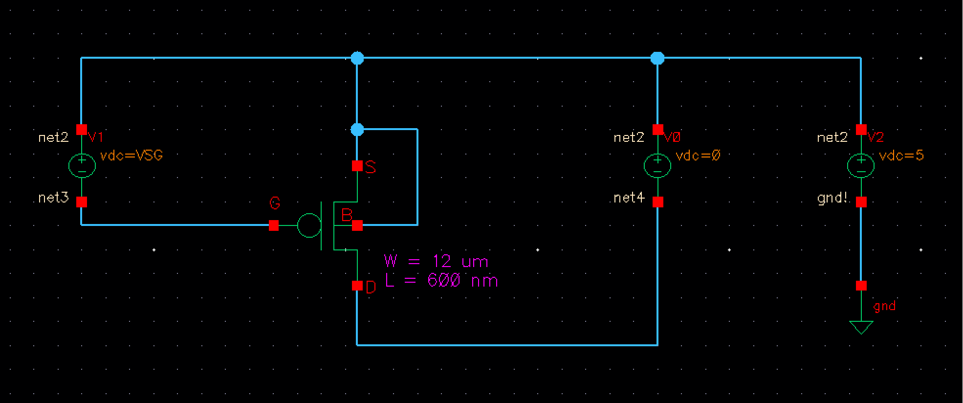
Let
us start off with the NMOS schematic and simulations. Below you will
see the circuit schematic created. I instantiated a nmos with 4
terminals to get use to selecting this in the future when laying out
our transistors as specified by Dr. Baker. Note that the bulk is tied
to ground.
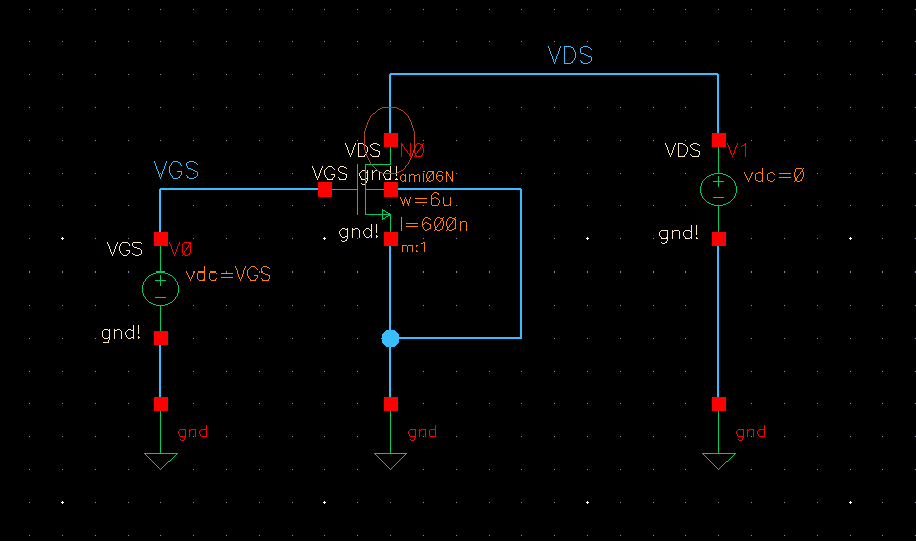
In
the image above you will notice that I have set the DC value of VGS as
"VGS". This will serve as our variable that we will need when
simulating the ID v. VDS with varying VGS voltage as the parameters
specified. For my convenience I will list the steps taken to set up the
graph.
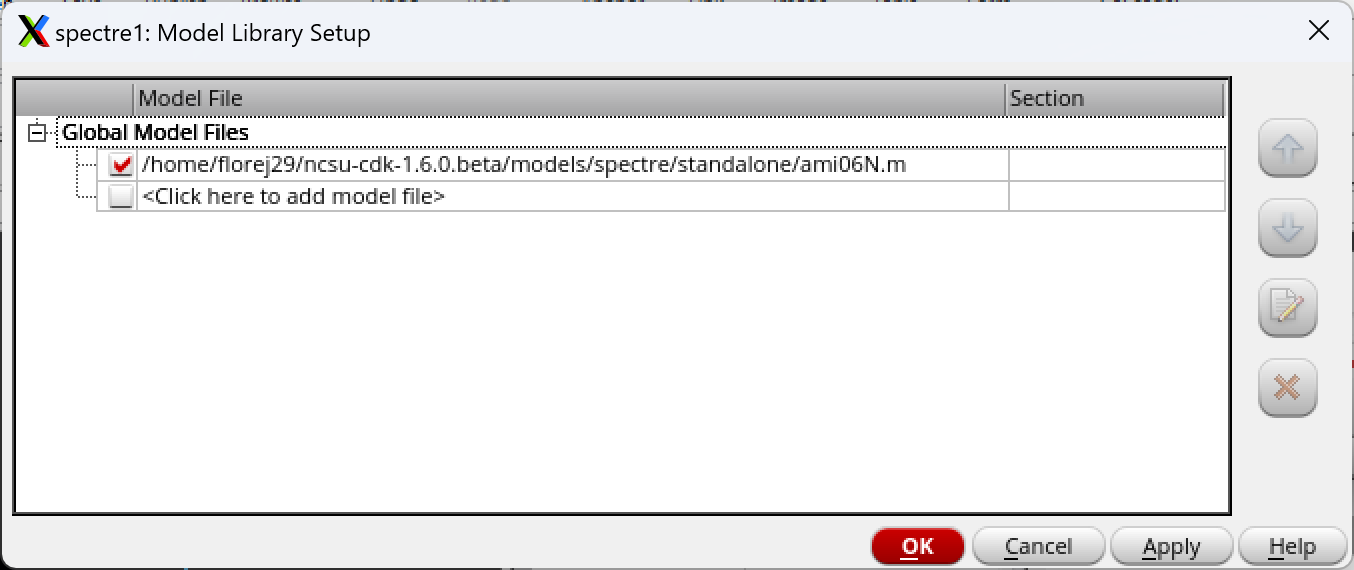
Now
that we have our net values named, we can launch ADE L. The very first
thing to do is verify that our simulator is in spectre. We then can
navigate to Setup -> Model Libraries, and browse to
directory->
/$HOME /ncsu-cdk-1.6.0.beta/models/spectre/standalone <- and
Select
ami06N.m (NMOS model). When we get to simulating the PMOS, we will
select the ami06P.m for the PMOS model.
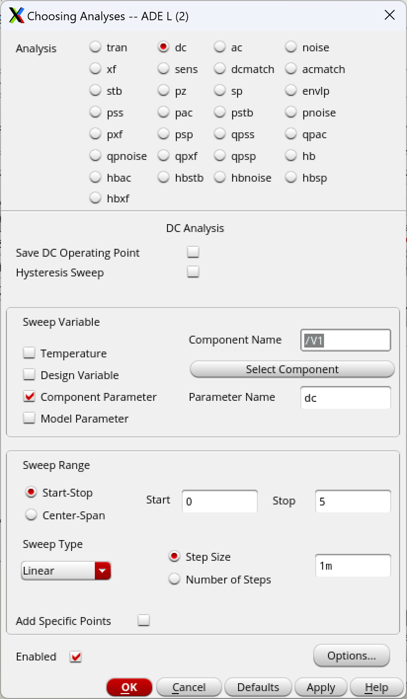
We
can then setup our dc sweep settings to the specified parameters on VDS
as seen below:
Now
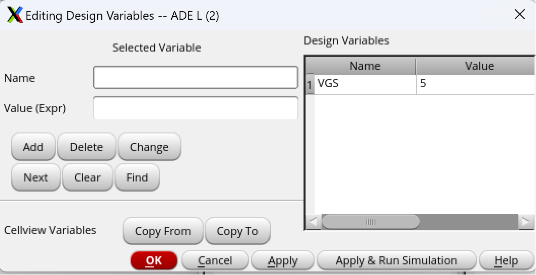
we must setup our variable VGS. In our ADE window, we navigate to
Variables -> Edit, and then add VGS:
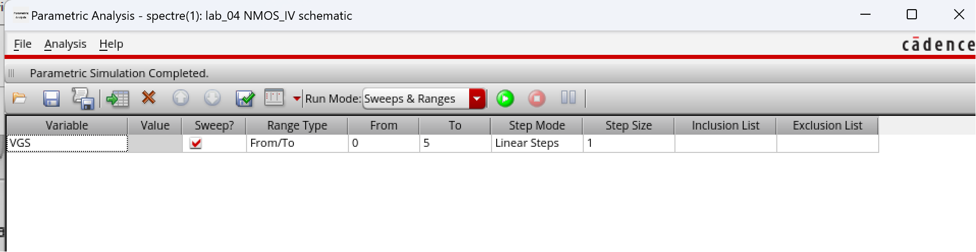
Finally,
in our ADE window again, we can navigate to Tools -> Parametric
Analysis, and setup the parameters to what was specified:
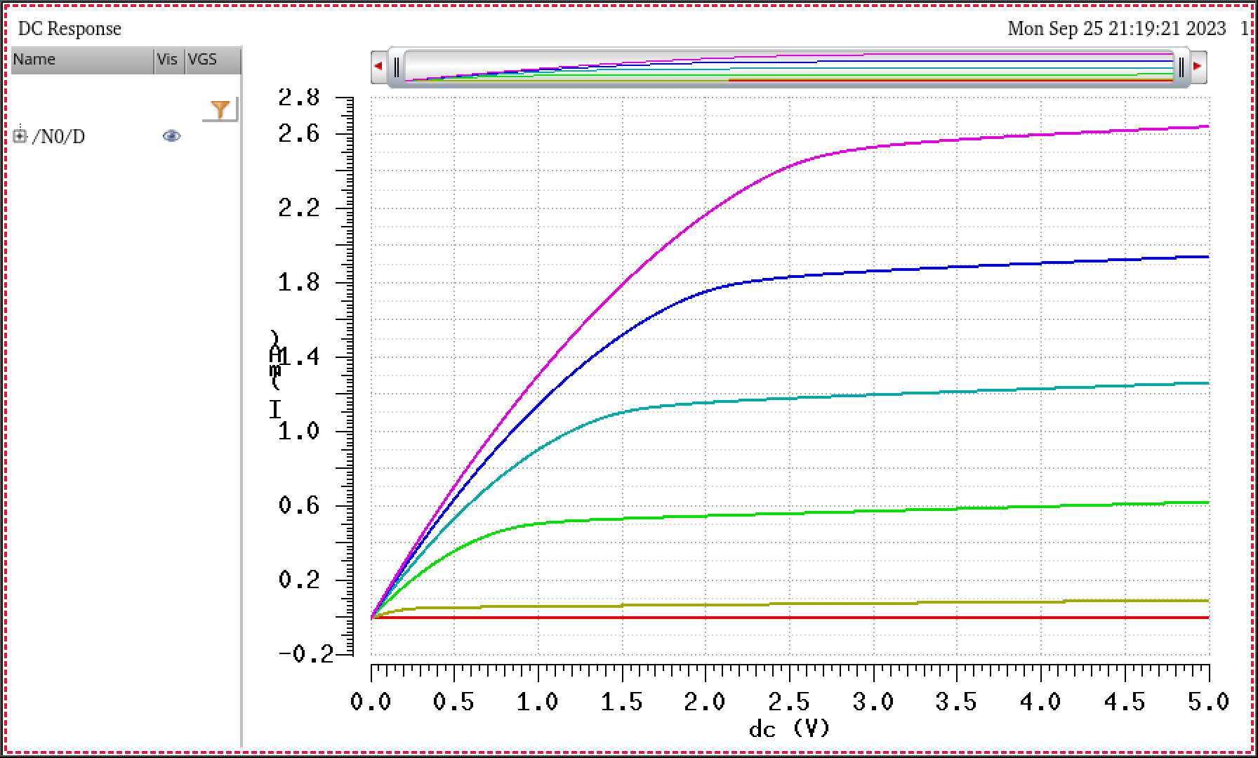
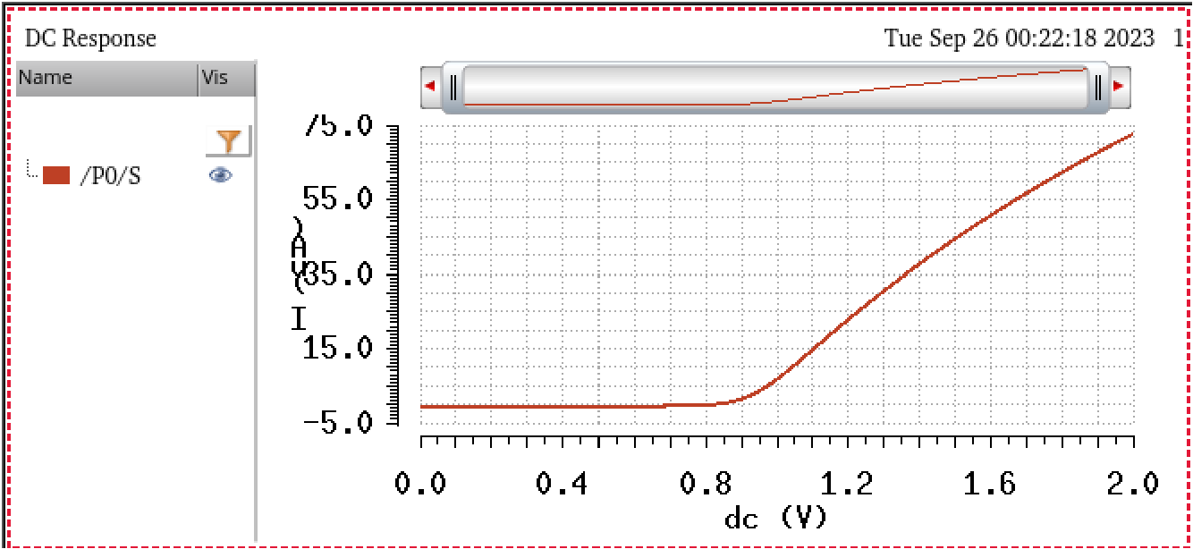
Our final result simulations yields the following:
ID v.
VDS with varying VGS
This
process can then be repeated for the rest of the simulations. I will
list out the required material for the sake of grading below.
Summary
of All Simulations
- A
schematic for simulating ID
v. VDS of an NMOS device for VGS varying from 0 to 5 V in 1 V steps
while VDS varies from 0 to 5 V in 1 mV steps. Use a 6u/600n
width-to-length ratio.
- A
schematic for simulating ID v. VGS of an NMOS device for VDS = 100 mV
where VGS varies from 0 to 2 V in 1 mV steps. Again use a 6u/600n
width-to-length ratio. Notice that we are keeping the width-to-length
ration the same, but we are keeping VDS at a constant value, while VGS
varies.
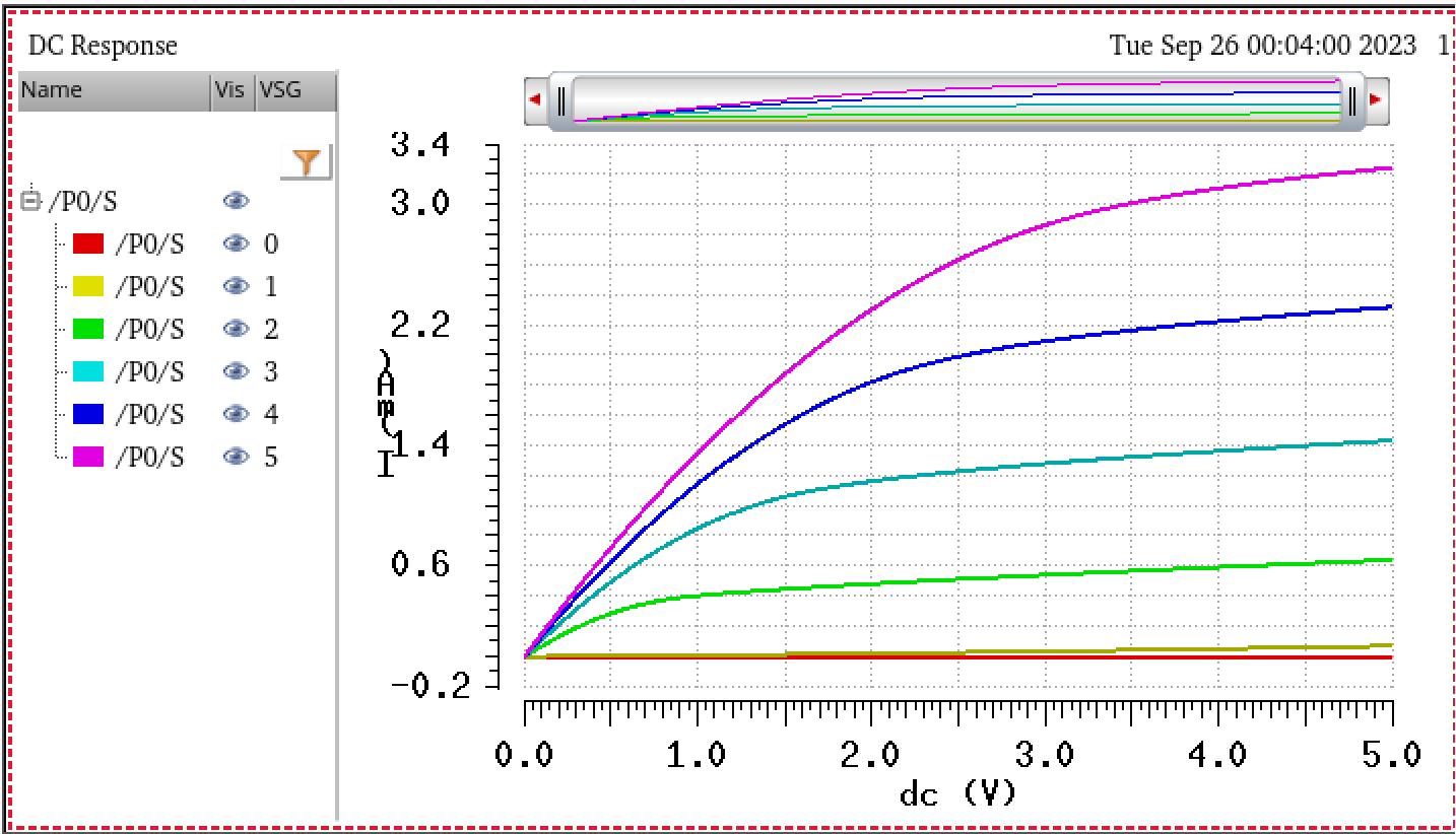
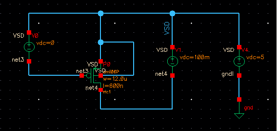
- A
schematic for simulating ID v. VSD (note VSD not VDS) of a PMOS device
for VSG (not VGS) varying from 0 to 5 V in 1 V steps while VSD varies
from 0 to 5 V in 1 mV steps. Use a 12u/600n
width-to-length
ratio. Note that in this simulation, the PMOS now has a different
width-to-length ratio, and our body is connected to vdd.
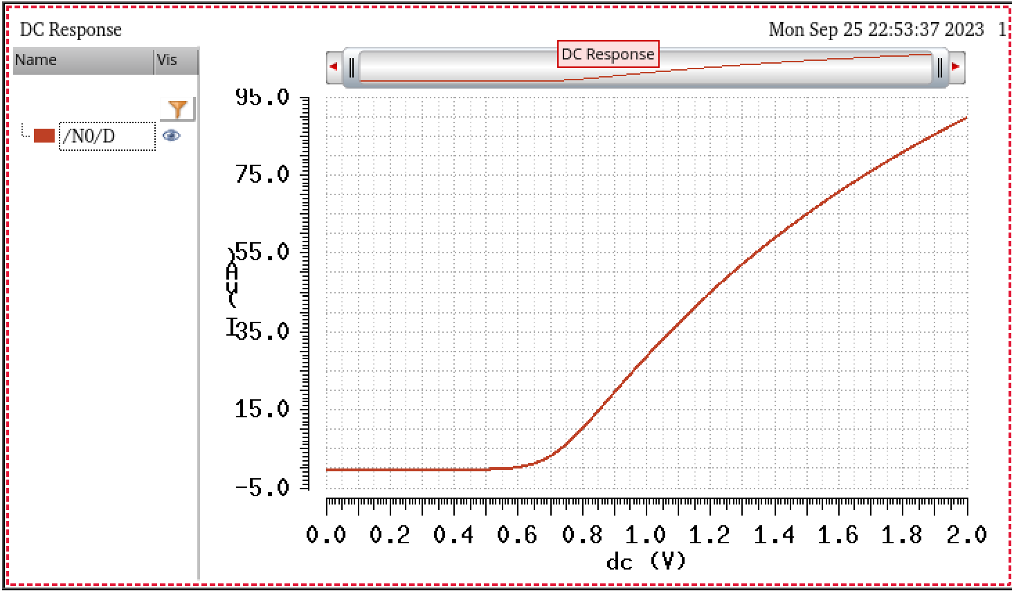
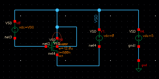
- A
schematic for simulating ID v. VSG of a PMOS device for VSD = 100 mV
where VSG varies from 0 to 2 V in 1 mV steps. Again, use a 12u/600n
width-to-length ratio. Similarly, like we did with the NMOS during this
step, we will do the same with this PMOS. No changes in the PMOS,
besides keeping VSD constant, and varying VSG.
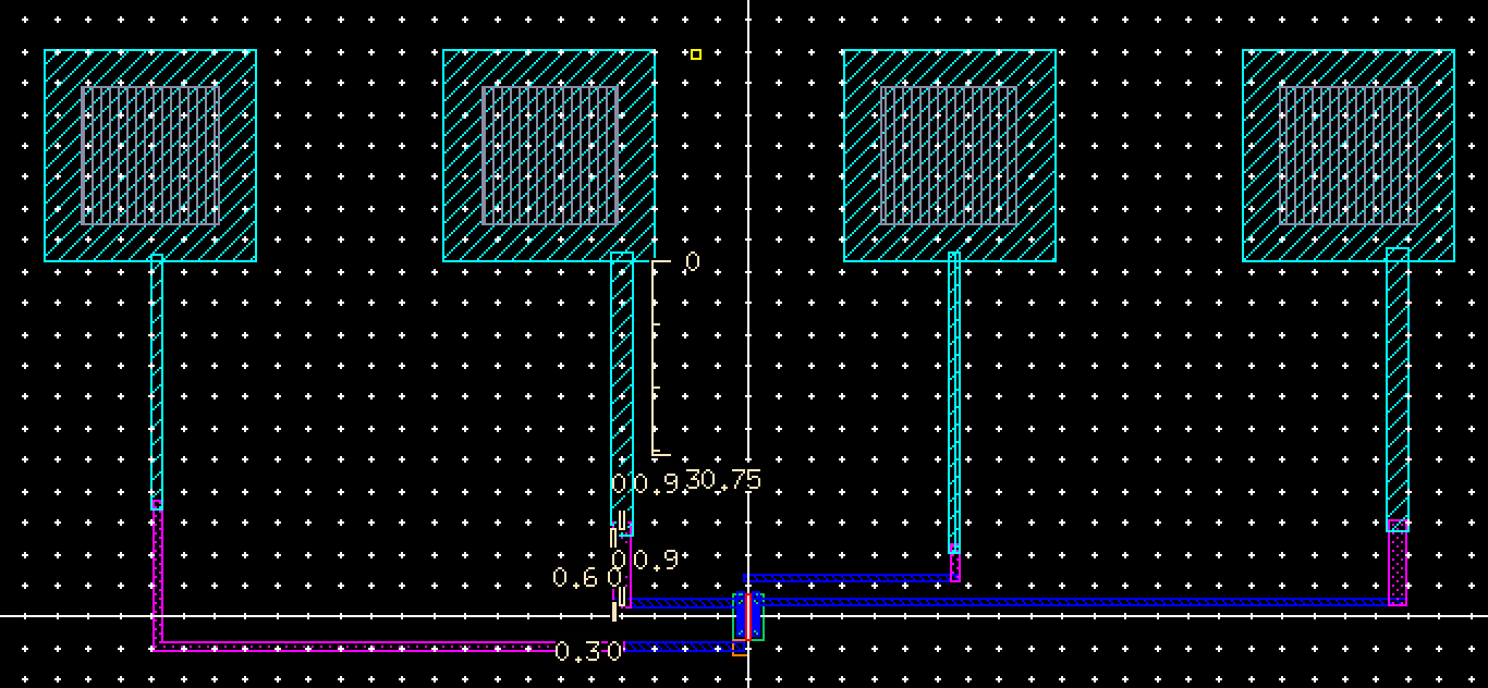
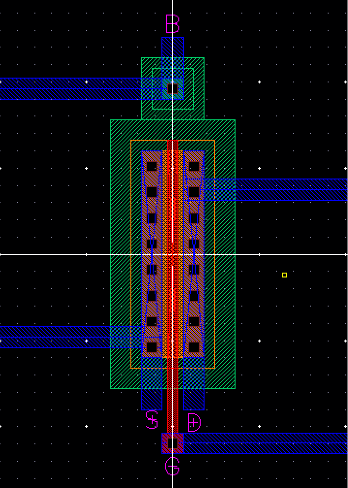
Layout
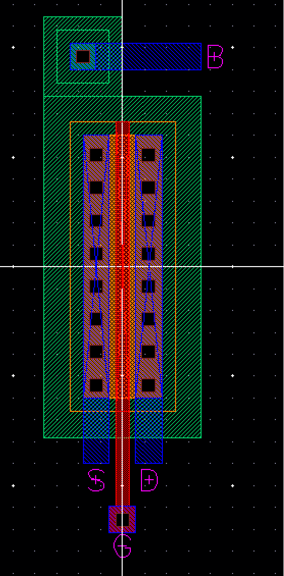
of NMOS
- Lay
out a 6u/0.6u NMOS device and connect all 4 MOSFET terminals to probe
pads (which can be considerably smaller than bond pads [see MOSIS
design rules] and directly adjacent to the MOSFET
(so the layout is relative small).
- Show your
layout passes DRCs.
- Make a
corresponding schematic so you can LVS your layout.
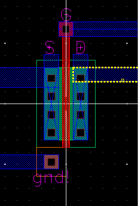
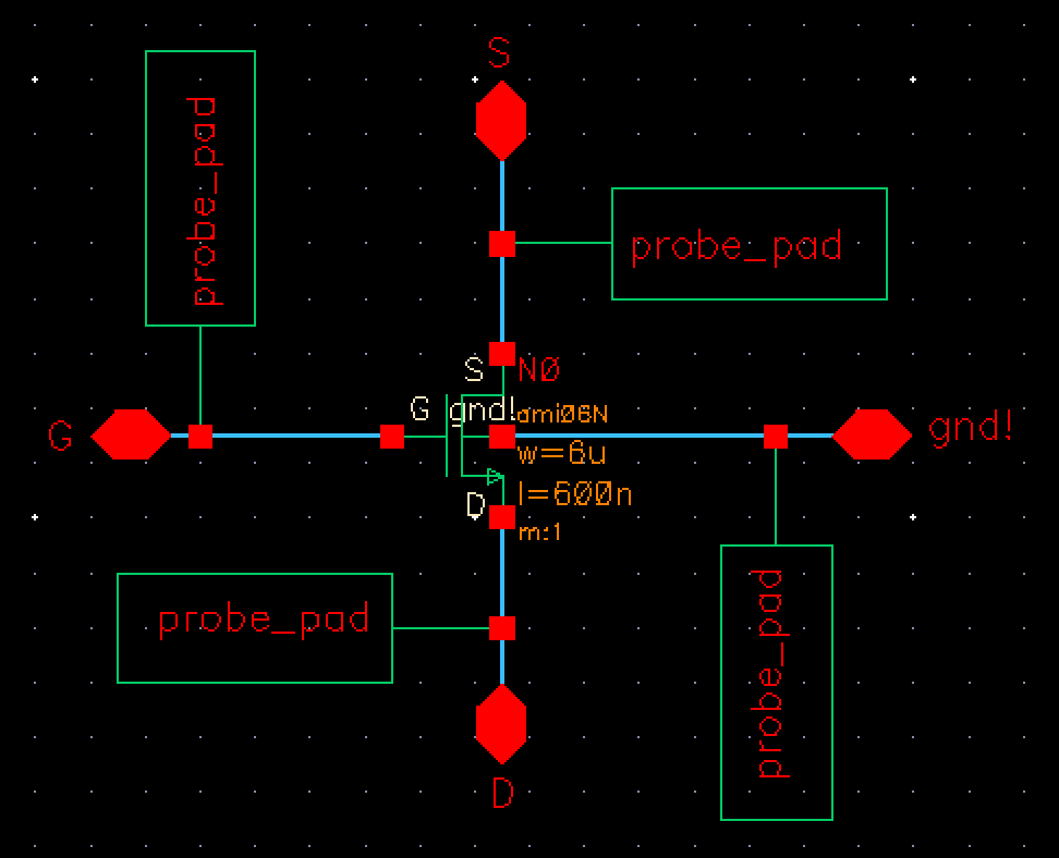
Schematic:
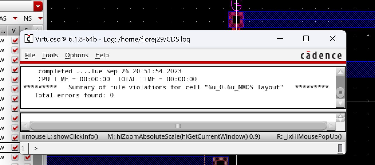
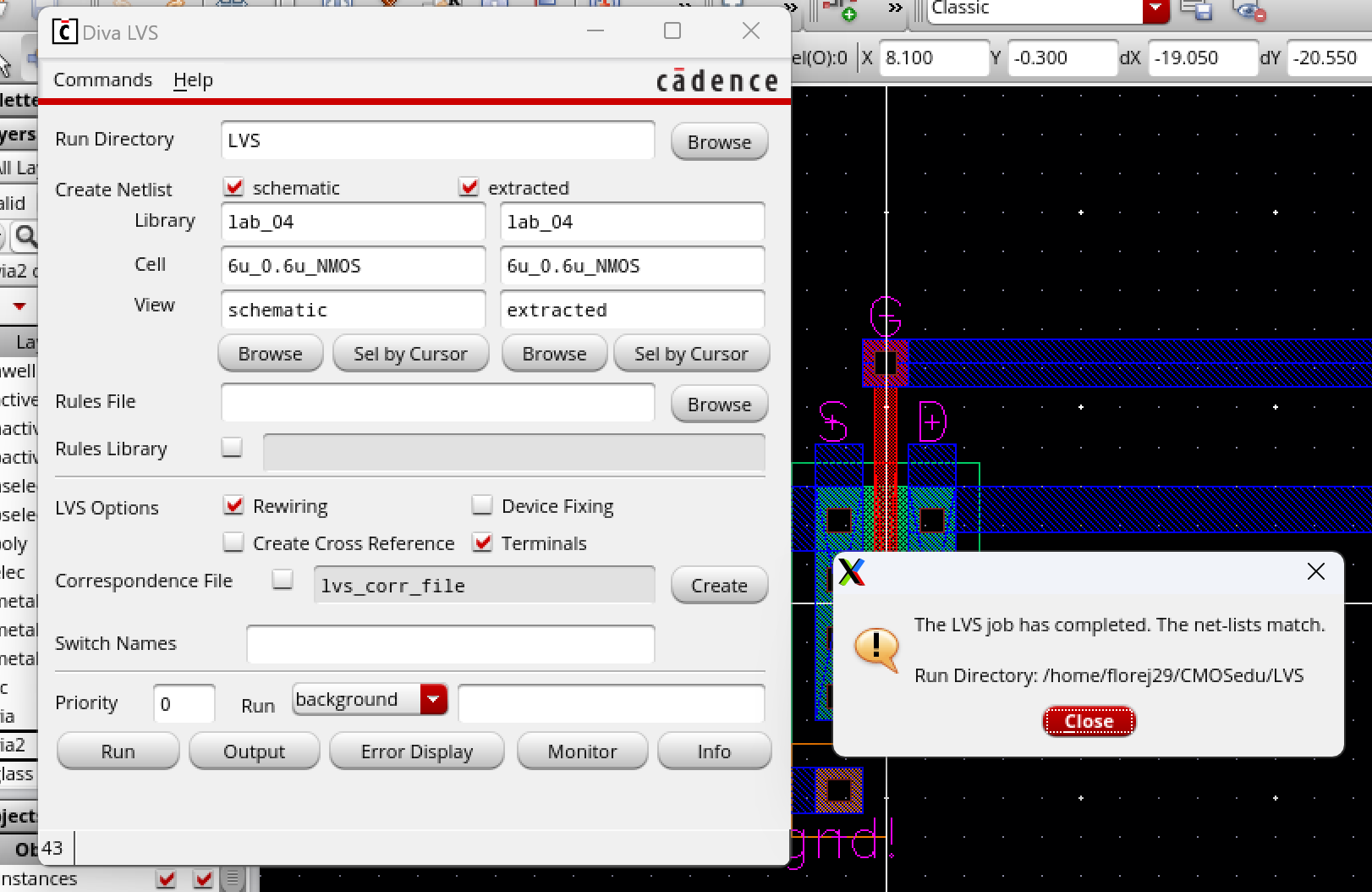
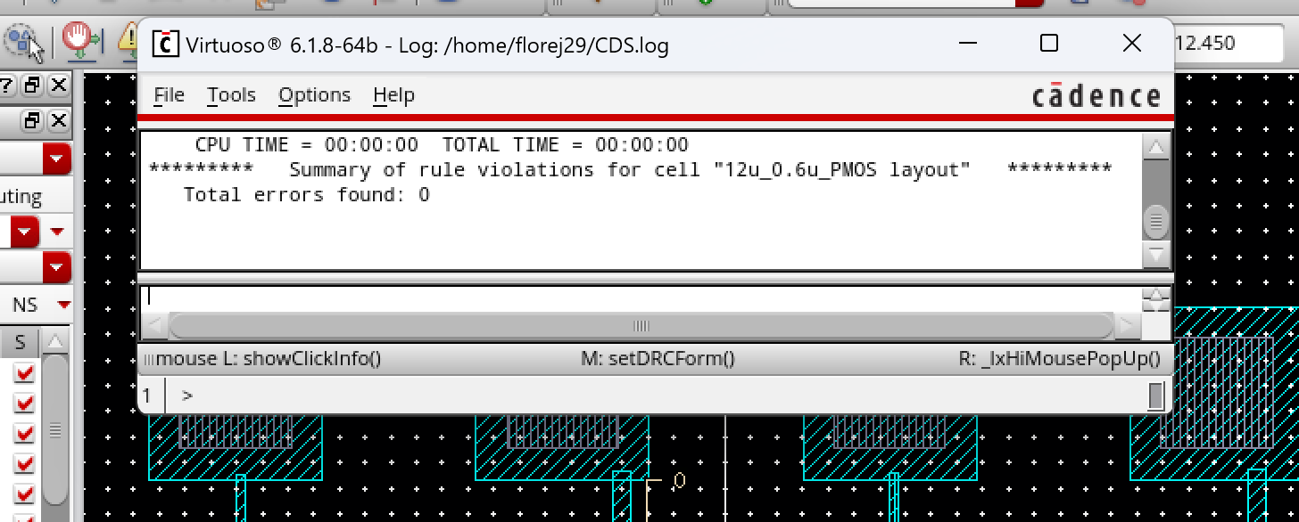
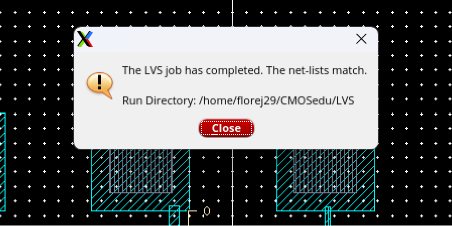
DRC
and LVS Pass below:
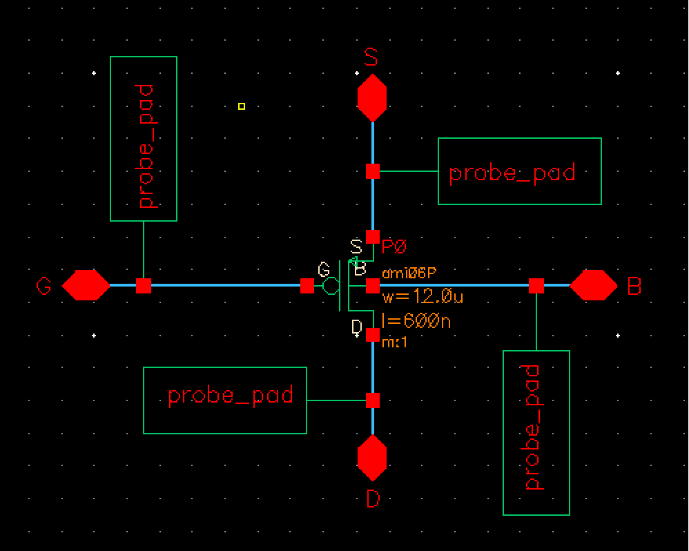
Layout of PMOS
- Lay out a
12u/0.6u PMOS device and connect all 4 MOSFET terminals to probe
pads.
- Show your
layout passes DRCs.
- Make a
corresponding schematic so you can LVS your layout.
Schematic:
DRC and LVS Pass:
As
you can see in the summary above for all simulations, all tests have
passed with no errors. This concludes Lab 4. You can find my
lab
files below for everything used in my simulations.
>> lab04.zip
<<
Return
to florej29 Lab Reports
Return
to Fall 2023 EE421L Student Lab Reports
Return
to Fall 2023 Digital Integrated Circuit Design Laboratory Home Page