Lab 3 - EE 421L
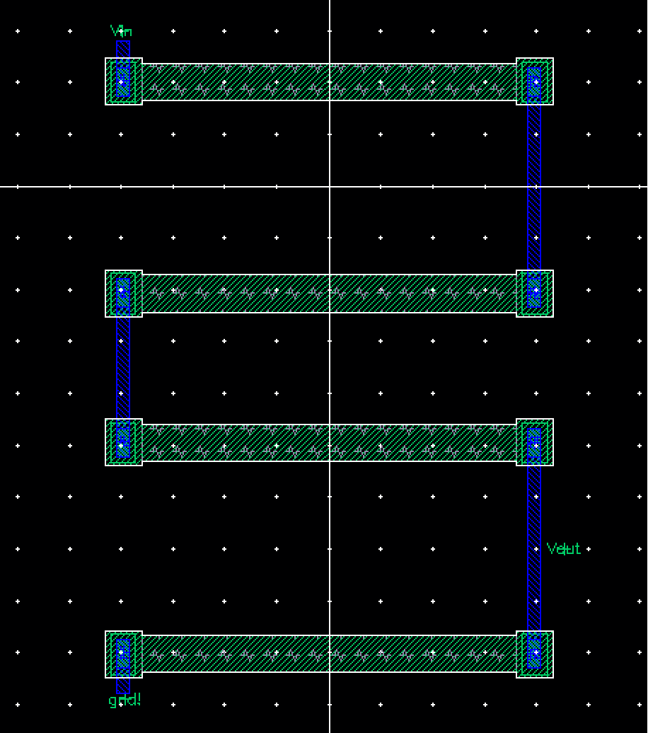
Below is the layout:
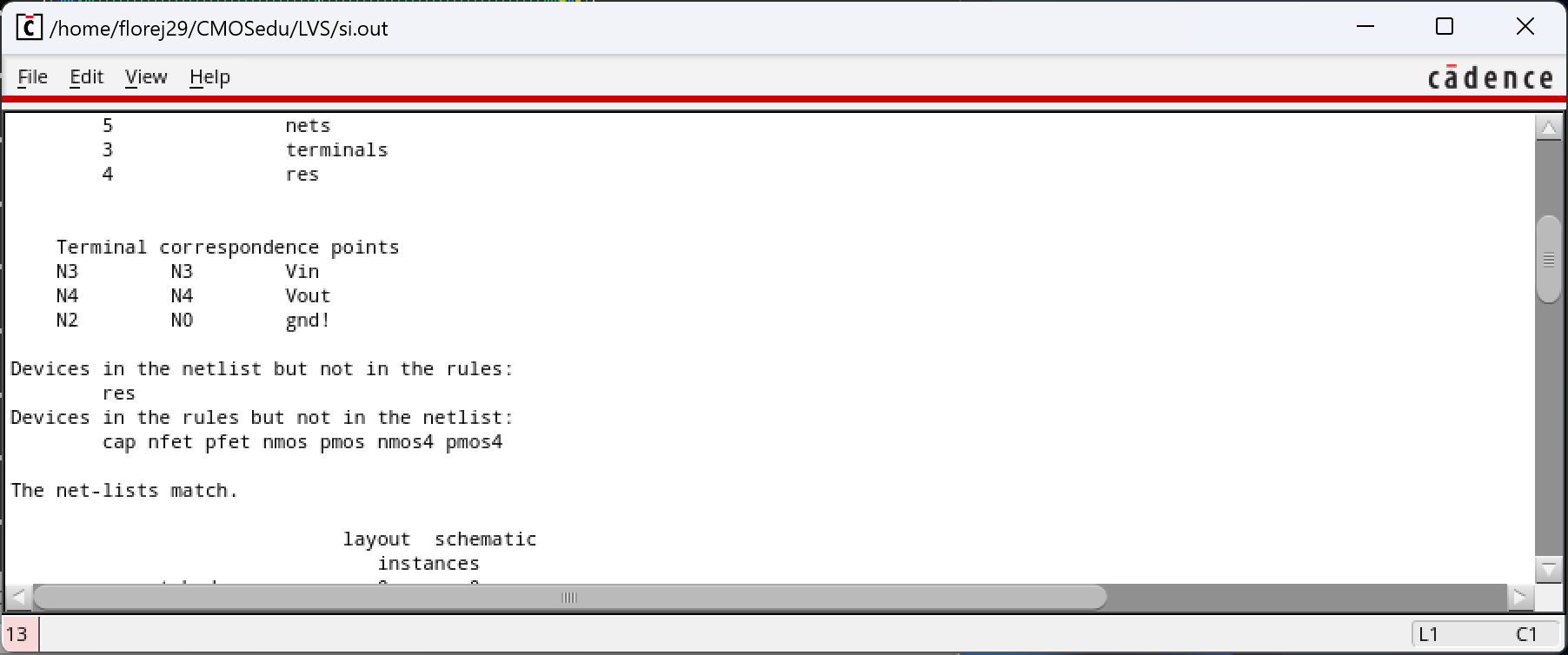
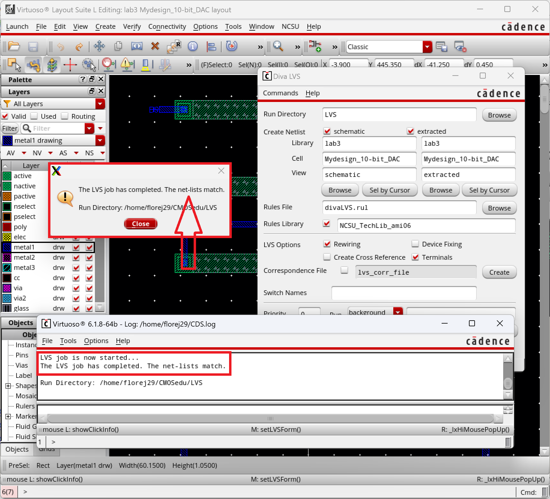
Here is the LVS showing the netlists match:
Lab Objectives
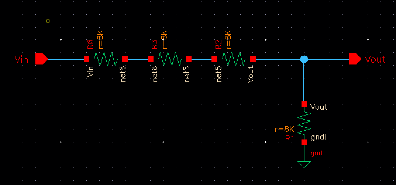
- We will the n-well to make a 10k resistor and use it to design our 10-bit DAC
- LVS our layout design with our schametic DAC made in lab2
Lab
For a C5 process, the sheet resistance is roughly 800 ohms, and we will use the minimum width of the n-well forr our resistar (i.e 3.6um). Recall the total resistance we want is 10k ohms.
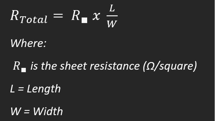
Solving for the length of our n-well yields the following.:
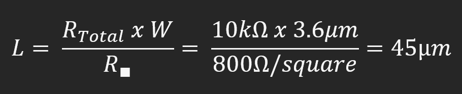
With that said, our n-well dimmensions are W = 3.6um, L = 45um. Keep in mind that our our dimmensions should be divisible by 0.15um, since our X and Y snap grid spacing is set to 0.15um. In this case, both lengths are divisible by 0.15, so no need for change.
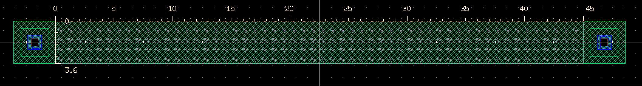
As seen above, our dimmensions are L = 45um and W = 3.6um. Note that I used the ruler command to show the lengths seen in the image above. To do this, you simply use the keyboard shortcut, k,. To get accurate measurements, while on the ruler tool, you can zoom in to a corner by pressing key, z, and selecting your area, click on the oorner, and zoom back out. Do the same for the other side to selec the second point of measurement.
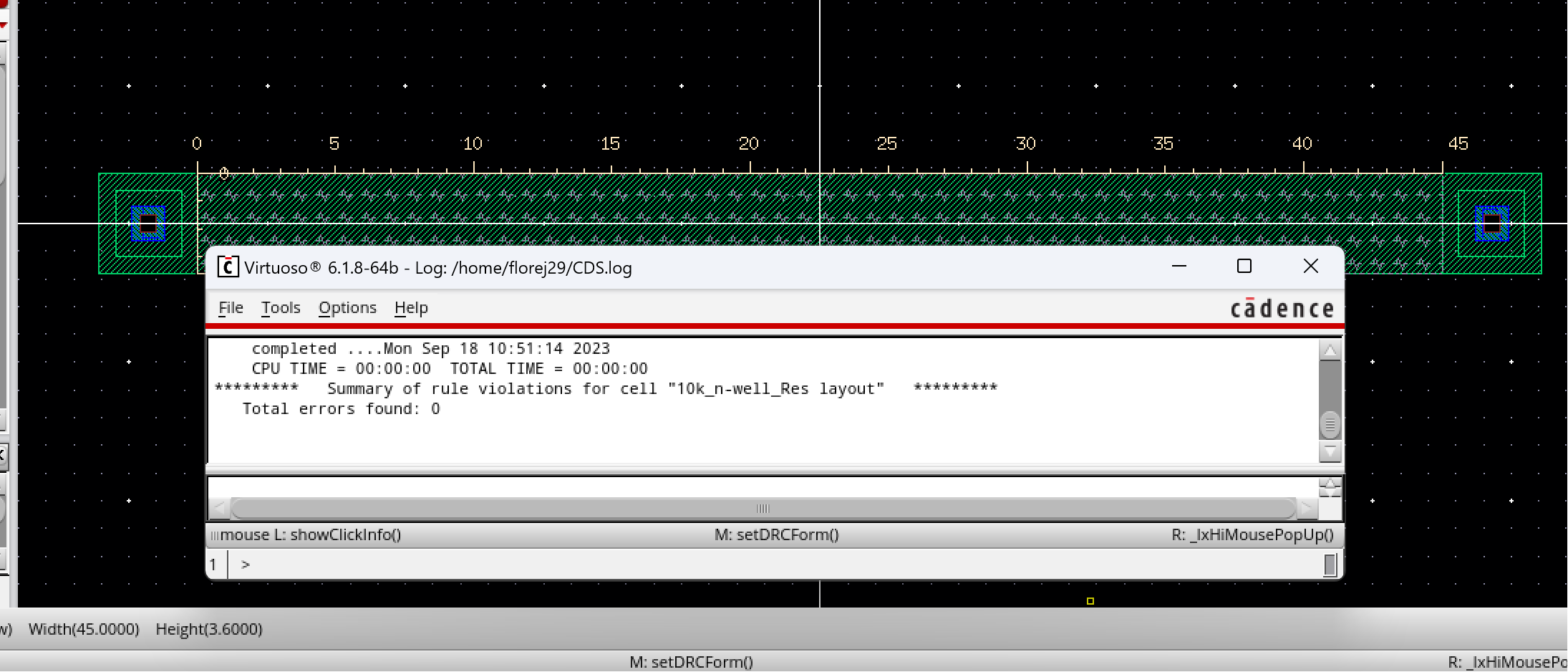
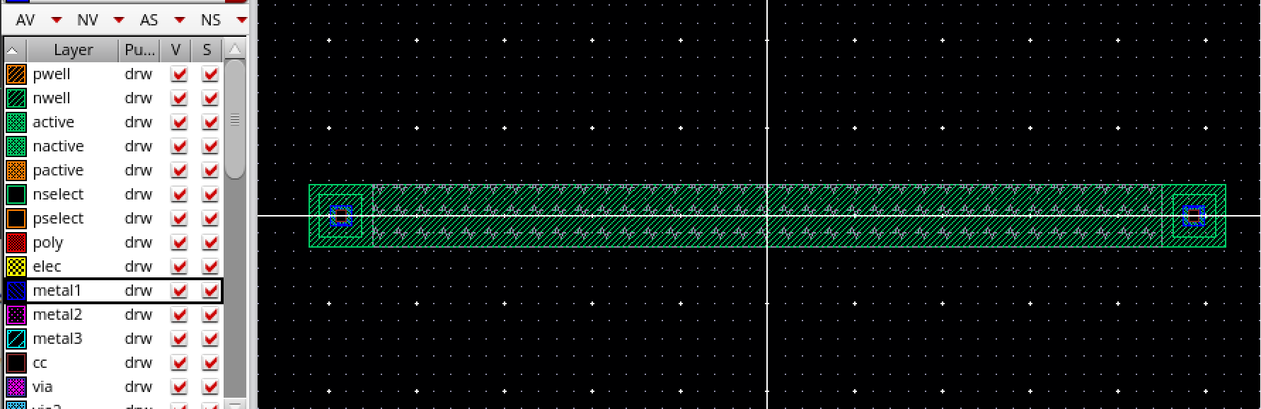
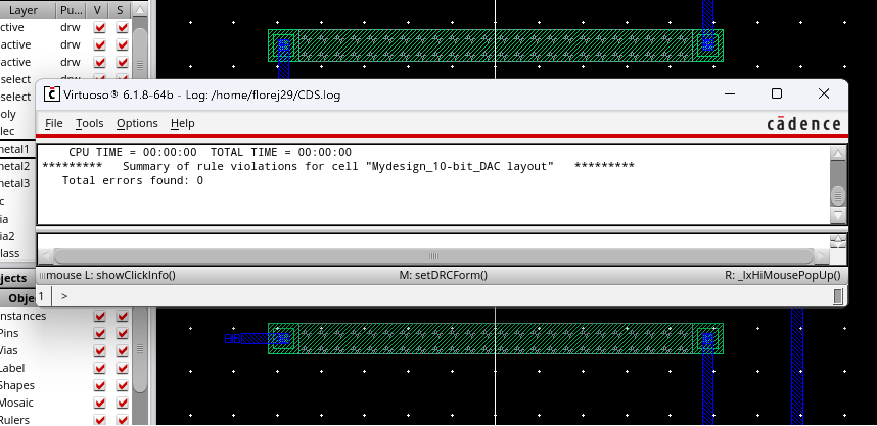
After creating the left and right pins with metal 1, and choosing the area of the resistor with the "res_id" drawing, we can DRC our resistor layout. Below you can see a clean DRC:
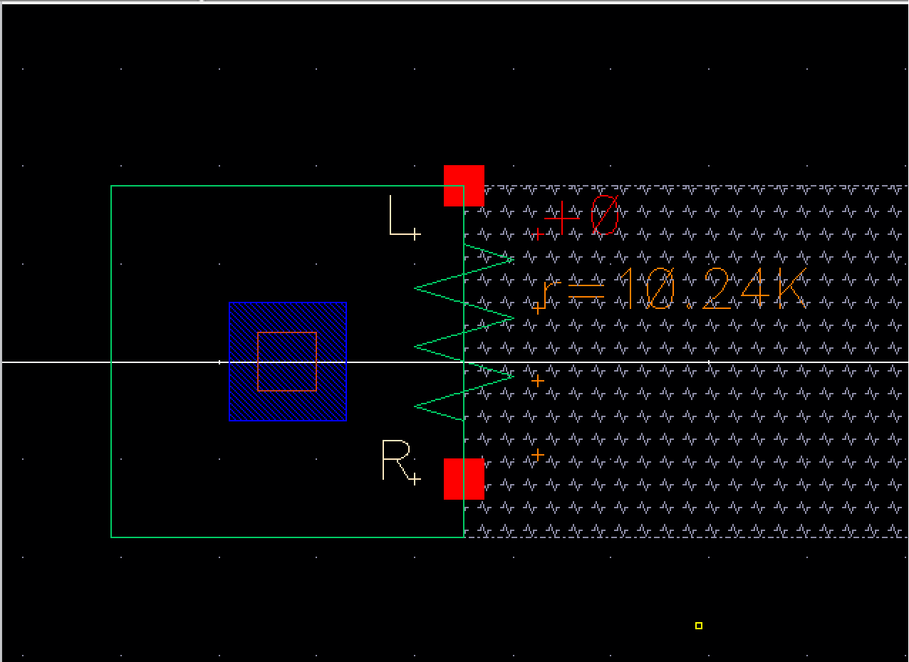
Our extracted value is the following:
We can finally design our 10-bit DAC using this 10k n-well resitor we just created.
We'll create a new layout inside our 10-bit DAC schematic cell design that was previously made in lab2. We can start by placing one single n-well centered at the origin.
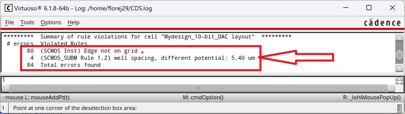
Before placing more resistors it is important to note that in the rules for this process we must space esach resistor with a minimum of 5.4um, or else we will get errors from the command window as seen below:
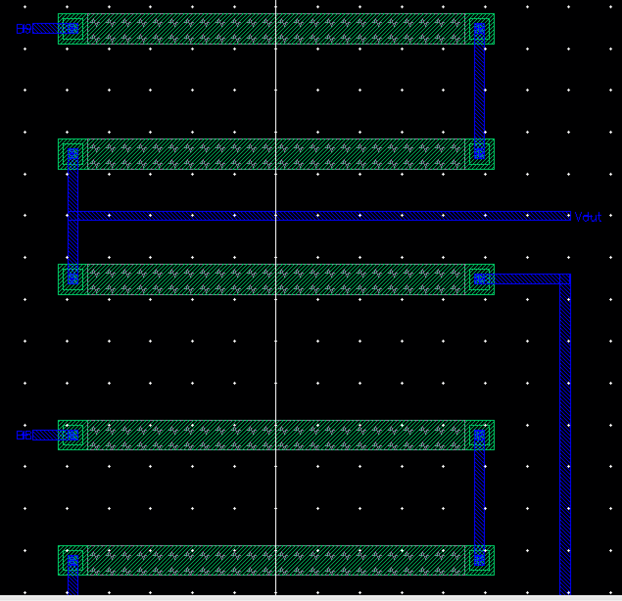
To avoid this issue, I spaced my resistors about 15um apart, center to center. This also allowed me to snap my pins and metal 1 wires to fit the grid snap requirements. After laying out all31, 10k n-well resistors as specified from the lab instructions, and connecting them according to our schematic for the DAC design, we get the following:
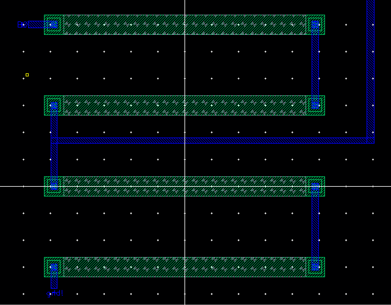
The above image shows the start of the resistor stack, and the below image shows the end where you can see bit 8 and bit 9, along with Vout.
Now we DRC our design for the final time:
After passing the DRC with no errors, we can finally LVS our layout. Here is my result:
That concludes this labs experiment. All tests have passed with a clean DRC and LVS. You can find my zipped file for this lab below.
>> lab3.zip <<